As and Epitaxial-Growth MnSi Thin Films - OPUS Würzburg
As and Epitaxial-Growth MnSi Thin Films - OPUS Würzburg
As and Epitaxial-Growth MnSi Thin Films - OPUS Würzburg

You also want an ePaper? Increase the reach of your titles
YUMPU automatically turns print PDFs into web optimized ePapers that Google loves.
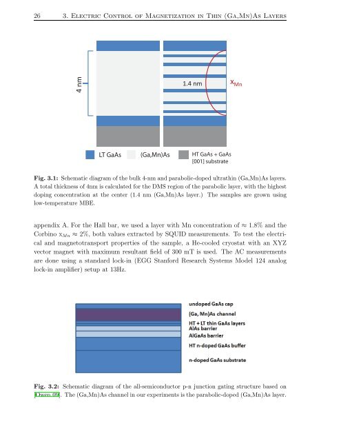
26 3. Electric Control of Magnetization in <strong>Thin</strong> (Ga,Mn)<strong>As</strong> Layers<br />
4 nm<br />
1.4 nm x Mn<br />
LT Ga<strong>As</strong> (Ga,Mn)<strong>As</strong> HT Ga<strong>As</strong> + Ga<strong>As</strong><br />
[001] substrate<br />
Fig. 3.1: Schematic diagram of the bulk4-nm <strong>and</strong>parabolic-doped ultrathin (Ga,Mn)<strong>As</strong> layers.<br />
A total thickness of 4nm is calculated for the DMS region of the parabolic layer, with the highest<br />
doping concentration at the center (1.4 nm (Ga,Mn)<strong>As</strong> layer.) The samples are grown using<br />
low-temperature MBE.<br />
appendix A. For the Hall bar, we used a layer with Mn concentration of ≈ 1.8% <strong>and</strong> the<br />
Corbino x Mn ≈ 2%, both values extracted by SQUID measurements. To test the electrical<br />
<strong>and</strong> magnetotransport properties of the sample, a He-cooled cryostat with an XYZ<br />
vector magnet with maximum resultant field of 300 mT is used. The AC measurements<br />
are done using a st<strong>and</strong>ard lock-in (EGG Stanford Research Systems Model 124 analog<br />
lock-in amplifier) setup at 13Hz.<br />
Fig. 3.2: Schematic diagram of the all-semiconductor p-n junction gating structure based on<br />
[Owen 09]. The (Ga,Mn)<strong>As</strong> channel in our experiments is theparabolic-doped (Ga,Mn)<strong>As</strong> layer.