As and Epitaxial-Growth MnSi Thin Films - OPUS Würzburg
As and Epitaxial-Growth MnSi Thin Films - OPUS Würzburg
As and Epitaxial-Growth MnSi Thin Films - OPUS Würzburg

Create successful ePaper yourself
Turn your PDF publications into a flip-book with our unique Google optimized e-Paper software.
6.2. Material Characterization 71<br />
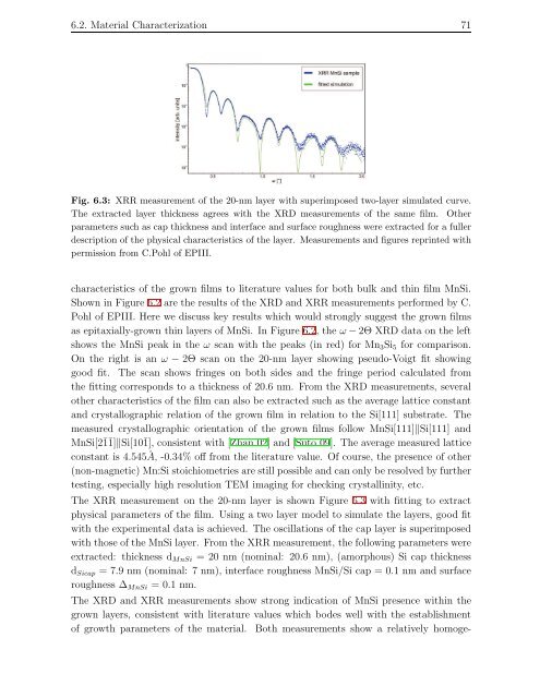
Fig. 6.3: XRR measurement of the 20-nm layer with superimposed two-layer simulated curve.<br />
The extracted layer thickness agrees with the XRD measurements of the same film. Other<br />
parameters such as cap thickness <strong>and</strong> interface <strong>and</strong> surface roughness were extracted for a fuller<br />
description of the physical characteristics of the layer. Measurements <strong>and</strong> figures reprinted with<br />
permission from C.Pohl of EPIII.<br />
characteristics of the grown films to literature values for both bulk <strong>and</strong> thin film <strong>MnSi</strong>.<br />
Shown in Figure 6.2 are the results of the XRD <strong>and</strong> XRR measurements performed by C.<br />
Pohl of EPIII. Here we discuss key results which would strongly suggest the grown films<br />
as epitaxially-grown thin layers of <strong>MnSi</strong>. In Figure 6.2, the ω−2Θ XRD data on the left<br />
shows the <strong>MnSi</strong> peak in the ω scan with the peaks (in red) for Mn 3 Si 5 for comparison.<br />
On the right is an ω − 2Θ scan on the 20-nm layer showing pseudo-Voigt fit showing<br />
good fit. The scan shows fringes on both sides <strong>and</strong> the fringe period calculated from<br />
the fitting corresponds to a thickness of 20.6 nm. From the XRD measurements, several<br />
other characteristics of the film can also be extracted such as the average lattice constant<br />
<strong>and</strong> crystallographic relation of the grown film in relation to the Si[111] substrate. The<br />
measured crystallographic orientation of the grown films follow <strong>MnSi</strong>[111]‖Si[111] <strong>and</strong><br />
<strong>MnSi</strong>[2¯1¯1]‖Si[10¯1], consistent with [Zhan 02] <strong>and</strong> [Suto 09]. The average measured lattice<br />
constant is 4.545Å, -0.34% off from the literature value. Of course, the presence of other<br />
(non-magnetic) Mn:Si stoichiometries arestill possible <strong>and</strong>canonly beresolved by further<br />
testing, especially high resolution TEM imaging for checking crystallinity, etc.<br />
The XRR measurement on the 20-nm layer is shown Figure 6.3 with fitting to extract<br />
physical parameters of the film. Using a two layer model to simulate the layers, good fit<br />
with the experimental data is achieved. The oscillations of the cap layer is superimposed<br />
with those of the <strong>MnSi</strong> layer. Fromthe XRR measurement, the following parameters were<br />
extracted: thickness d <strong>MnSi</strong> = 20 nm (nominal: 20.6 nm), (amorphous) Si cap thickness<br />
d Sicap = 7.9 nm (nominal: 7 nm), interface roughness <strong>MnSi</strong>/Si cap = 0.1 nm <strong>and</strong> surface<br />
roughness ∆ <strong>MnSi</strong> = 0.1 nm.<br />
The XRD <strong>and</strong> XRR measurements show strong indication of <strong>MnSi</strong> presence within the<br />
grown layers, consistent with literature values which bodes well with the establishment<br />
of growth parameters of the material. Both measurements show a relatively homoge-