FREE DVD
FREE DVD
FREE DVD

You also want an ePaper? Increase the reach of your titles
YUMPU automatically turns print PDFs into web optimized ePapers that Google loves.
gger/Programmer<br />
does have the advantage that the additional<br />
hardware required for debugging<br />
is generally no more than a communications<br />
module between the host<br />
processor and the development system,<br />
making it simple and cost-effective<br />
to achieve.<br />
To enable the code alterations resulting<br />
from this program development to<br />
be transferred directly into the host<br />
hardware, an In-Circuit Debugger is<br />
generally combined with a programming<br />
module known as an In-Circuit<br />
Programmer (ICP). Enhancing the program<br />
development environment with a<br />
test and programming setup of the<br />
kind described in this article provides a<br />
single integrated user interface for program<br />
generation, transfer, translation<br />
and testing in the host hardware.<br />
ICD2<br />
Starting point for this exercise was<br />
Microchip’s ICD2 module, the circuit<br />
of which is given in [4]. The aim was<br />
to reduce this design to its basic<br />
functionality so as to achieve a device<br />
that was reproducible and cost-effective<br />
but still widely compatible with<br />
the original. This was achieved by<br />
specifying:<br />
• 5V power for the module derived<br />
from the host device<br />
•<br />
Dispensing with interface drivers<br />
between ICD module and host<br />
hardware<br />
Fixed programming voltage<br />
•<br />
Confining the communications<br />
interface to RS-232 protocol<br />
TGT MCLR/THV<br />
+VCC<br />
+VCC<br />
K2<br />
1<br />
2<br />
3<br />
4<br />
5<br />
+VCC<br />
TGT PGD<br />
+VCC<br />
R10<br />
10k<br />
R25<br />
10k<br />
R13<br />
10k<br />
R14<br />
RC0<br />
RC1<br />
C11<br />
100n<br />
1<br />
16<br />
IN1<br />
IN2<br />
12<br />
VL<br />
IC2<br />
V+<br />
13<br />
S1<br />
D1<br />
3<br />
2<br />
S2<br />
14<br />
D2 15<br />
6<br />
TGT PGC<br />
GND<br />
D4<br />
4k7<br />
5V6<br />
400mW<br />
R12<br />
4k7<br />
R16<br />
1k<br />
D7<br />
POWER<br />
10k<br />
R2<br />
+VCC<br />
C7<br />
100n<br />
R19<br />
RC2<br />
+VCC<br />
R21<br />
9<br />
8<br />
S3<br />
11<br />
IN3<br />
D3 10<br />
DG411DJ<br />
S4<br />
6<br />
IN4<br />
D4<br />
7<br />
GND V-<br />
5<br />
4<br />
11<br />
32<br />
6k8<br />
4k7<br />
K1<br />
SUB D9<br />
1<br />
6<br />
2<br />
7<br />
3<br />
8<br />
4<br />
9<br />
5<br />
R4<br />
DTR<br />
1k<br />
1µ<br />
25V<br />
C1<br />
RXD<br />
RTS<br />
TXD<br />
CTS<br />
C2<br />
1µ<br />
25V<br />
C3<br />
1µ<br />
25V<br />
2<br />
1<br />
C1+<br />
V+<br />
16<br />
3 IC4<br />
C1–<br />
7<br />
T2OUT T2IN<br />
10<br />
13<br />
8<br />
R1IN<br />
R2IN<br />
R1OUT<br />
R2OUT<br />
12<br />
9<br />
14<br />
T1OUT T1IN<br />
11<br />
4<br />
C2+<br />
5<br />
C2–<br />
D2<br />
D1 2x<br />
1N4148<br />
MAX232<br />
V-<br />
6<br />
15<br />
C4<br />
1µ<br />
25V<br />
R17<br />
220 Ω<br />
R11<br />
220 Ω<br />
R15<br />
220 Ω<br />
+VCC<br />
C5<br />
1µ<br />
C12<br />
100n<br />
D5<br />
ERROR<br />
1k<br />
R8<br />
1<br />
MCLR/THV<br />
RA0/AN0<br />
RA1/AN1<br />
15<br />
RC0<br />
RA2/AN2<br />
16<br />
17<br />
18<br />
RC1<br />
RC2<br />
RC3<br />
RA3/AN3<br />
RA4/T0CKI<br />
RA5/AN4<br />
23<br />
RC4<br />
24<br />
IC1<br />
RC5<br />
RD7<br />
25<br />
TX/RC6<br />
RD6<br />
26<br />
RX/RC7<br />
RD5<br />
RD4<br />
33<br />
INT/RB0<br />
RD3<br />
34<br />
RB1<br />
RD2<br />
35 PIC16F877<br />
RB2<br />
RD1<br />
36<br />
37<br />
38<br />
39<br />
40<br />
RB3/PGM<br />
RB4<br />
RB5<br />
RB6/PGC<br />
RB7/PGD<br />
RD0<br />
RE0/RD/AN5<br />
RE1/WR/AN6<br />
RE2/CS/AN7<br />
OSC1 OSC2<br />
12 13 14 31<br />
R9<br />
X1<br />
1k<br />
270 Ω<br />
R3<br />
D6 C9<br />
20MHz<br />
C8<br />
BUSY 22p<br />
22p<br />
2<br />
3<br />
4<br />
5<br />
6<br />
7<br />
30<br />
29<br />
28<br />
27<br />
22<br />
21<br />
20<br />
19<br />
8<br />
9<br />
10<br />
2k2<br />
C14<br />
1n<br />
R20<br />
1 Ω<br />
4k7<br />
R5<br />
R22<br />
2k2<br />
R24<br />
+VCC<br />
IC3 6<br />
C13<br />
100n<br />
L1<br />
330µH<br />
7<br />
1<br />
I SENS SWI COL<br />
3<br />
8<br />
TIM CAP DRI COL<br />
MC34063A<br />
2<br />
5<br />
SWI EMI COMP IN<br />
4<br />
R7<br />
1k<br />
R23<br />
6k8<br />
68Ω<br />
D3<br />
1N5819<br />
R6<br />
10k<br />
R1<br />
VPROG<br />
33Ω<br />
R18<br />
C6<br />
10µ<br />
25V<br />
C10<br />
100n<br />
050348 - 11<br />
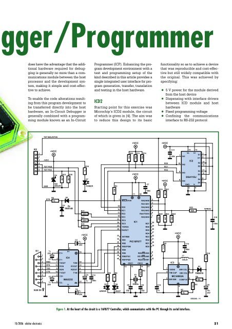
Figure 1. At the heart of the circuit is a 16F877 Controller, which communicates with the PC through its serial interface.<br />
10/2006 - elektor electronics 51