FREE DVD
FREE DVD
FREE DVD

Create successful ePaper yourself
Turn your PDF publications into a flip-book with our unique Google optimized e-Paper software.
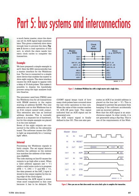
Part 5: bus systems and interconnections<br />
a much faster master, since the slave<br />
can set its ACK signal high sometime<br />
later. This gives a relatively slow slave<br />
enough time to process the data. Figure<br />
2 shows a read operation of this<br />
sort, in which the slave needs two<br />
extra clock cycles to complete the<br />
transaction.<br />
Master<br />
(e. g. 8052)<br />
CLK I<br />
Clock<br />
and<br />
Reset<br />
Slave<br />
(e. g. OUTPUT)<br />
CLK I<br />
RST I<br />
RST I<br />
Example<br />
We have prepared a simple example in<br />
ex13. Here the 8051 microcontroller has<br />
a master interface for the Wishbone<br />
bus. The bus is connected to a simple<br />
slave device that enables the master to<br />
drive eight outputs. The slave interface<br />
causes the ACK signal to appear with<br />
a delay of 10 clock pulses. This makes it<br />
possible to display the handshake<br />
process using the logic analyser built<br />
into Quartus.<br />
DAT O7...O0<br />
DAT I7...I0<br />
DAT I7...I0<br />
DAT O7...O0<br />
ADR O15...O0<br />
ADR I15...I0<br />
WE O<br />
WE I<br />
STB O<br />
STB I<br />
CYC O<br />
CYC I<br />
ACK I<br />
ACK O<br />
060025 - 5 - 11<br />
Figure 1. A minimum Wishbone bus with a single master and a single slave.<br />
The processor used here (T8052) uses<br />
the Wishbone bus for all transactions<br />
with XRAM memory in the region<br />
starting at address 0x1000. The only<br />
extension unit on this Wishbone bus is<br />
an 8-bit output named wish_output.<br />
This extension also has an internal<br />
address decoder. This is normally<br />
placed in a separate bit of hardware,<br />
but for this simple example we placed<br />
it in the core instead.<br />
Seven of the eight outputs are connected<br />
to the LEDs on the extension<br />
board. The software causes the LEDs<br />
to light up sequentially for a ‘runninglight’<br />
effect.<br />
Master<br />
IN<br />
Slave<br />
IN<br />
CLK<br />
COUNT signal keeps track of how<br />
many clock pulses have occurred since<br />
the last write operation to this core.<br />
When the value of this counter reaches<br />
10, ACK_OK goes high. This signal<br />
indicates that an ACK signal can be<br />
generated now.<br />
The ACK output signal is finally<br />
defined in line 101. This core also generates<br />
an ACK if an invalid address is<br />
placed on the bus (sel = ‘0’). This is<br />
designed to prevent the processor from<br />
hanging if the software accidentally<br />
uses an incorrect address.<br />
Note that the ACK signal is an asynchronous<br />
signal. In other words, it is<br />
not generated using a flip-flop. This is<br />
one of the requirements of the Wish-<br />
Internal<br />
Processing the Wishbone signals is<br />
fairly simple. The sel signal detects<br />
whether the address on the system<br />
bus matches the address of the extension<br />
(0x8000).<br />
The code starting on line 63 causes the<br />
outputs to go high after a reset. When<br />
a valid address appears (sel = ‘1’)<br />
while a valid write cycle is in progress<br />
(STB = ‘1’, CYC = ‘1’ and WE = ‘1’),<br />
the data present at the DAT_I input is<br />
stored in the output register by the rising<br />
edge of the clock signal.<br />
Generating the ACK signal is somewhat<br />
more complicated in this case<br />
because it has to be delayed. The<br />
IN IN<br />
IN OUT<br />
OUT<br />
OUT<br />
OUT<br />
OUT<br />
IN<br />
IN<br />
IN<br />
IN<br />
IN<br />
OUT<br />
RESET<br />
DAT<br />
ADR<br />
WE<br />
CYC<br />
STB<br />
ACK<br />
XXXXX<br />
XX<br />
XX<br />
VALID<br />
VALID<br />
XX<br />
XX<br />
XX<br />
060025 - 5 - 12<br />
Figure 2. Here you can see that slave needs two extra clock cycles to complete the transaction.<br />
10/2006 - elektor electronics 61