SIOV Metal Oxide Varistors - DEMAR
SIOV Metal Oxide Varistors - DEMAR
SIOV Metal Oxide Varistors - DEMAR

You also want an ePaper? Increase the reach of your titles
YUMPU automatically turns print PDFs into web optimized ePapers that Google loves.
General Technical Information<br />
FRAME4/home/SMC-Archiv-DB/GG-KB-engl/DB-<strong>SIOV</strong>_97_BNR-B462-P6214-X-X-7600/Allgemeine<br />
The voltage dependence of varistors or VDRs (Voltage Dependent Resistors) is expressed by the<br />
nonlinearity exponent α. In metal oxide varistors it has been possible to produce α figures of more<br />
than 30. This puts their protection levels in the same region as those of zener diodes and suppressor<br />
diodes. Exceptional current handling capability combined with response times of < 25 ns (SMD<br />
< 0,5 ns) make them an almost perfect protective device.<br />
1.3 Microstructure and conduction mechanism<br />
Sintering zinc oxide together with other metal oxide additives under specific conditions produces a<br />
polycrystalline ceramic whose resistance exhibits a pronounced dependence on voltage. This<br />
phenomenon is called the varistor effect.<br />
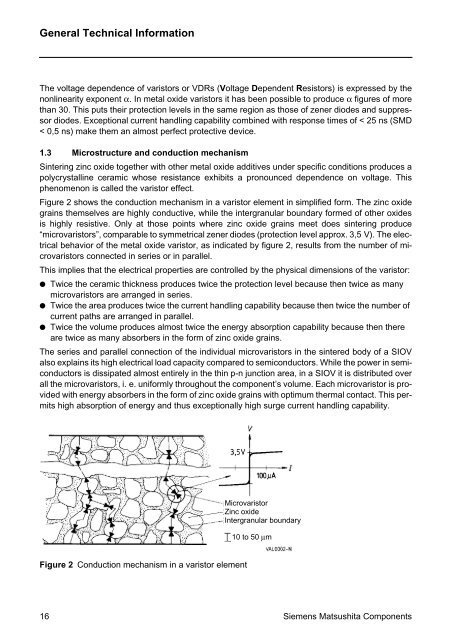
Figure 2 shows the conduction mechanism in a varistor element in simplified form. The zinc oxide<br />
grains themselves are highly conductive, while the intergranular boundary formed of other oxides<br />
is highly resistive. Only at those points where zinc oxide grains meet does sintering produce<br />
“microvaristors”, comparable to symmetrical zener diodes (protection level approx. 3,5 V). The electrical<br />
behavior of the metal oxide varistor, as indicated by figure 2, results from the number of microvaristors<br />
connected in series or in parallel.<br />
This implies that the electrical properties are controlled by the physical dimensions of the varistor:<br />
● Twice the ceramic thickness produces twice the protection level because then twice as many<br />
microvaristors are arranged in series.<br />
● Twice the area produces twice the current handling capability because then twice the number of<br />
current paths are arranged in parallel.<br />
● Twice the volume produces almost twice the energy absorption capability because then there<br />
are twice as many absorbers in the form of zinc oxide grains.<br />
The series and parallel connection of the individual microvaristors in the sintered body of a <strong>SIOV</strong><br />
also explains its high electrical load capacity compared to semiconductors. While the power in semiconductors<br />
is dissipated almost entirely in the thin p-n junction area, in a <strong>SIOV</strong> it is distributed over<br />
all the microvaristors, i. e. uniformly throughout the component’s volume. Each microvaristor is provided<br />
with energy absorbers in the form of zinc oxide grains with optimum thermal contact. This permits<br />
high absorption of energy and thus exceptionally high surge current handling capability.<br />
Figure 2 Conduction mechanism in a varistor element<br />
Microvaristor<br />
Zinc oxide<br />
Intergranular boundary<br />
10 to 50 µm<br />
16 Siemens Matsushita Components
![Equações Diferenciais Ordinárias Lineares de 2ª Ordem [ ] [ ] - DEMAR](https://img.yumpu.com/43234810/1/184x260/equaaaues-diferenciais-ordinarias-lineares-de-2a-ordem-demar.jpg?quality=85)