FS4400 PCI Express State Analysis Probe User Manual - FuturePlus ...
FS4400 PCI Express State Analysis Probe User Manual - FuturePlus ...
FS4400 PCI Express State Analysis Probe User Manual - FuturePlus ...

You also want an ePaper? Increase the reach of your titles
YUMPU automatically turns print PDFs into web optimized ePapers that Google loves.
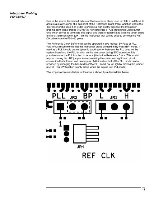
Interposer Probing<br />
FS1034/5/7<br />
Due to the source terminated nature of the Reference Clock used in <strong>PCI</strong>e it is difficult to<br />
acquire a quality signal at a mid-point of the Reference Clock trace, which is where the<br />
Interposer probe sees it. In order to provide a high quality signal at the Interposer<br />
probing point these probes (FS1034/5/7) incorporate a <strong>PCI</strong>e Reference Clock buffer<br />
chip which serves to terminate this signal and then re-transmit it to both the target board<br />
and to a 3 pin connector (JR1) on the Interposer that can be used to connect the Ref.<br />
Clk cable from the <strong>FS4400</strong> probe.<br />
The Reference Clock Buffer chip can be operated in two modes: By-Pass or PLL.<br />
<strong>FuturePlus</strong> recommends that the Interposer probe be used in By-Pass (BP) mode. If<br />
used as a PLL it could create dynamic tracking error between the PLL used on the<br />
system board and the PLL function on the interposer during SSC operation. It is<br />
possible to use the PLL function to reduce jitter in the Reference Clock. This would<br />
require moving the JR2 jumper from connecting the center and right hand pins to<br />
connection the left hand and center pins. Additional control of the PLL mode can be<br />
provided by changing the bandwidth of the PLL from Low to High by moving the jumper<br />
at JR3. This BW function is only active when the device is in PLL mode.<br />
The proper recommended shunt location is shown by a dashed line below:<br />
12