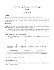
ECEN 454 â Lab1: Introduction to Cadence Schematic Capture ...
ECEN 454 â Lab1: Introduction to Cadence Schematic Capture ...
ECEN 454 â Lab1: Introduction to Cadence Schematic Capture ...

You also want an ePaper? Increase the reach of your titles
YUMPU automatically turns print PDFs into web optimized ePapers that Google loves.
<strong>ECEN</strong> <strong>454</strong> – <strong>Lab1</strong>: <strong>Introduction</strong> <strong>to</strong> <strong>Cadence</strong> <strong>Schematic</strong> <strong>Capture</strong> &<br />
Simulation<br />
We will now begin the design by implementing the logic design of the 8-bit Pipelined adder. The<br />
following sections introduce you <strong>to</strong> the procedures <strong>to</strong> use <strong>Cadence</strong> for schematic capture and<br />
simulation which you will use <strong>to</strong> implement the required logic design.<br />
1. <strong>Introduction</strong> <strong>to</strong> <strong>Cadence</strong> Tool<br />
By now you should have created a direc<strong>to</strong>ry called "cadence" in your home direc<strong>to</strong>ry<br />
and changed your working direc<strong>to</strong>ry <strong>to</strong> cadence. If not refer <strong>to</strong> Lab0 before you begin.<br />
To start <strong>Cadence</strong> type "icfb &". If you see “***/xlsfonts: not found”, disregard it. You<br />
can also see two pop-up windows telling you what’s new about this version of <strong>Cadence</strong>.<br />
Click ok. At the same time, a small rectangular window will pop up. This is called<br />
Command Interpreter Window (CIW). This is where icfb will display all the messages<br />
about your commands. Do not close this window (except when quitting!) and always<br />
keep this window visible. CIW displays all the error and warning messages, so please<br />
look in<strong>to</strong> this whenever possible. Also it will guide you what <strong>to</strong> do next. A window<br />
called Library Manager will also pop up.<br />
The heading of the CIW is icfb - Log: /homex/xxxx/CDS.log and has three menus File,<br />
Tools and Options. The lower left corner has the icfb prompt which displays ">", when<br />
it awaits next action.<br />
We can now create designs in icfb. It s<strong>to</strong>res all data in a library. A library can contain<br />
one or more designs. Designs in a library use a technology file, which describes the<br />
rules associated with the fabrication processes. So when we create a new library, the<br />
first thing which should be done is <strong>to</strong> attach a technology file <strong>to</strong> a new library. To create<br />
a new library, open Library Manager thru Tools > Library Manager in CIW, then<br />
choose File > New. You will see three items when you do “left click” on New: Library,<br />
Cellview, and Category. Library is the <strong>to</strong>p concept in hierarchical structure. And below<br />
are cells with several different properties. For physical layout design, the Cellview<br />
name is layout. If it is a gate level design, the Cellview name is schematic. For<br />
transis<strong>to</strong>r level design, we use cmos.sch. We have also “extracted”, and “symbol”<br />
which will be used in the following labs.<br />
<br />
Icfb uses Library Manager for browsing through all the libraries. The Library Manager<br />
has several libraries including any designs created by you. Several other pre-designed<br />
libraries are also required before your own design. Please open a web-browser (e.g.,<br />
>firefox &), go <strong>to</strong> lab webpage, and download a file named “cds.lib” <strong>to</strong> save it in your<br />
cadence direc<strong>to</strong>ry. In the Library Manager window, select Edit > Library Path, and you<br />
will see the Library Path Edi<strong>to</strong>r window pops up. In the window, select File > Open <strong>to</strong><br />
find and select the “cds.lib” file just saved in your cadence direc<strong>to</strong>ry, click it, and press<br />
OK. You can simply ignore warning messages about unlocked file. If the “cds.lib” file<br />
is well launched, you will see the Library path Edi<strong>to</strong>r window as below.<br />
Texas A & M University Page 1
<strong>ECEN</strong> <strong>454</strong> – <strong>Lab1</strong>: <strong>Introduction</strong> <strong>to</strong> <strong>Cadence</strong> <strong>Schematic</strong> <strong>Capture</strong> &<br />
Simulation<br />
At the Library Manager window, click File > New > Library and type in name “Design”<br />
as shown below. Click OK.<br />
Next, you will find a menu for technology file. Choose “Attach <strong>to</strong> an existing techfile”<br />
and click OK. Then choose “NCSU_TechLib_tsmc02” as shown below. It means from<br />
now when you design a device, you will do it according <strong>to</strong> the rules related <strong>to</strong> this<br />
technology<br />
Texas A & M University Page 2
<strong>ECEN</strong> <strong>454</strong> – <strong>Lab1</strong>: <strong>Introduction</strong> <strong>to</strong> <strong>Cadence</strong> <strong>Schematic</strong> <strong>Capture</strong> &<br />
Simulation<br />
A library contains more than one design. Icfb calls each design a cell. For example there<br />
can be one cell for ALU, one cell for a flip-flop, and so on. In this lab we will design a<br />
one-bit adder. So let’s create a new cell called "fulladder". For this click on the<br />
“Design” library in the Library Manager window and choose File New > Cell view.<br />
Type cell name and view name. (Figures are just reference only. Do type as it shows)<br />
In the Cell Name field, type "fulladder". As mentioned, above there can be several<br />
designs in a library and cadence s<strong>to</strong>res each design as a cell. Also each cell can be<br />
represented in many ways for example as gate level or transis<strong>to</strong>r level schematics,<br />
layouts, SPICE netlists or verilog etc. Icfb calls these representations as cellviews.<br />
Since a design can be represented in many ways i.e. there can be many cellviews for a<br />
cell.<br />
For the adder design we will create a gate level schematic. This is called a "schematic<br />
view". In the view name field, type "schematic". Click OK on the form and a schematic<br />
view is created.<br />
Click on the fulladder cell in the Library Manager and you can see the schematic cell<br />
view ("fulladder schematic"). By now you should be clear with cells and cell views, if<br />
not ask your TA. Also look back and see the procedure for creating cells and cell views.<br />
This is the general procedure and you must remember it.<br />
2. <strong>Schematic</strong> of the Fulladder Circuit.<br />
The full adder is the basic building block of the 4-bit adder block that we need <strong>to</strong> design which<br />
we will eventually use <strong>to</strong> create the 8-bit Pipelined adder. The method is <strong>to</strong> create the design<br />
(schematic in this case) of the lowest building block (fulladder) and create a “symbol” of this<br />
design which can be reused in some other design (we would be using it in a higher level design<br />
<strong>to</strong> create a 4-bit adder)<br />
Texas A & M University Page 3
<strong>ECEN</strong> <strong>454</strong> – <strong>Lab1</strong>: <strong>Introduction</strong> <strong>to</strong> <strong>Cadence</strong> <strong>Schematic</strong> <strong>Capture</strong> &<br />
Simulation<br />
We can now create the first design - a gate-level schematic of 1-bit full adder. The adder<br />
will take three inputs: A, B and C (carry-in). The output will be two bits: SUM and<br />
CARRY. If you are not aware of the truth table for the adder, ask your TA.<br />
From the truth table the SUM and the CARRY functions can be generated. This can be<br />
simplified <strong>to</strong> CARRY = AB + (A XOR B) C and SUM = (A) XOR (B) XOR (C).<br />
To start the <strong>Cadence</strong> schematic edi<strong>to</strong>r, called Virtuoso, (if it is not already open), hold<br />
the middle mouse but<strong>to</strong>n on the schematic cellview of fulladder in the library Manager,<br />
scroll down and choose "Open". At most of time the edi<strong>to</strong>r will pop up au<strong>to</strong>matically<br />
when you add the new cell. This is where you design your schematic. To create an<br />
instance of a gate, choose Add → Instance from the edi<strong>to</strong>r menu. Component Browser<br />
(CB) and Add Instance window pops up.<br />
Choose library “NCSU_Digital_Parts” in CB. You will see lots of items like And, Flipflops,<br />
etc. You can choose any gate you want from this list. If you want OR gate, click<br />
“OR” in CB. You will see OR2, OR3… OR6. Choose OR2 if you want 2 inputs OR<br />
gate. If you click OR2, the Add Instance window will be au<strong>to</strong>matically filled. Move<br />
your mouse <strong>to</strong> Virtuoso window and click at the point where you want <strong>to</strong> place the OR<br />
gate. One more click you will have one more OR gate. Press ESC if you do not want<br />
OR gate any more.<br />
NOTE: Use only XOR and NAND2 (you will have <strong>to</strong> figure out how <strong>to</strong> replace the AND and OR<br />
gates with only NAND2 gates) for the full adder. This is <strong>to</strong> maintain consistency among all<br />
Texas A & M University Page 4
<strong>ECEN</strong> <strong>454</strong> – <strong>Lab1</strong>: <strong>Introduction</strong> <strong>to</strong> <strong>Cadence</strong> <strong>Schematic</strong> <strong>Capture</strong> &<br />
Simulation<br />
students and it also means you have <strong>to</strong> implement only the XOR and NAND2 layouts.<br />
(Remember: step 2 in section 2 of Lab0 will ask you <strong>to</strong> implement layouts of all the logic gates<br />
you used in the schematic design. Not only will you have <strong>to</strong> design fewer layouts (NAND2 instead<br />
of AND and OR) but also the implementation of a NAND2 layout can be easier than that of an<br />
AND or OR layout as you will find in the following weeks).<br />
Also, try <strong>to</strong> minimize the number of gates used in your design. A fulladder circuit can be<br />
composed of <strong>to</strong>tally 5 gates of XOR and NAND2.<br />
Place as many instances of this gate as required. When you finish press ESC key. If you<br />
have placed some extra instances then go <strong>to</strong> Edit > Delete in the Composer menu and<br />
click on the instance <strong>to</strong> delete. To exit from the Delete mode press ESC. To save the<br />
design click on Design > Save. Always save your work when you finish some important<br />
operations. When completing design, click Design > Check and Save option <strong>to</strong> verify it.<br />
Place instances of all the gates required and make you familiar with Add Instance and<br />
Delete Instance functions. Make sure you have plenty of space left for wiring your<br />
schematic. You can Zoom In and out <strong>to</strong> fit a part or whole of your design using<br />
Window → Zoom → Zoom In and Zoom Out respectively.<br />
We now have <strong>to</strong> wire the design. Before that we need <strong>to</strong> place input and output pins. The<br />
pins are for the input output connection of this design and also help for the simulation.<br />
We need five pins, three input pins A, B, C and two output pins SUM and CARRY.<br />
Select Add → Pin in the Virtuoso menu. Add Pin form pops up. Type “A B C ” in the<br />
Pin Names field. Make sure that the Direction of the pin is “input”. Go <strong>to</strong> the schematic<br />
window and place the three input pins wherever you feel appropriate. (You might have<br />
<strong>to</strong> zoom).<br />
Note that the pins A, B and C are different from the A, B and C you see on the instances<br />
of the gates. These (the later) are for the gates themselves, one level below the<br />
hierarchy. In the same way, create the output pins “SUM and CARRY” but remember<br />
<strong>to</strong> change the direction field in the Add Pin form <strong>to</strong> “output”.<br />
Texas A & M University Page 5
<strong>ECEN</strong> <strong>454</strong> – <strong>Lab1</strong>: <strong>Introduction</strong> <strong>to</strong> <strong>Cadence</strong> <strong>Schematic</strong> <strong>Capture</strong> &<br />
Simulation<br />
Before wiring let’s see some Composer functions. You can move and copy the instances<br />
using Edit > Move and Edit > Copy functions. Also you can undo the changes made<br />
using Edit > Undo. The CIW and the lower corner of the Composer will guide you.<br />
Finally let’s wire the schematic. Choose “Add > Wire (narrow)” in the window. Click on<br />
the A pin, a wire follows you. Take it <strong>to</strong> the point you want it <strong>to</strong> go and notice that the<br />
edi<strong>to</strong>r does au<strong>to</strong>matic routing for you. Place it at the output of the proper gate. Similarly<br />
wire the rest of the circuit. Note that the wires can overlap without making contacts<br />
unless you explicitly do so. To make sure you wire <strong>to</strong> the exact place you want, notice<br />
that there is a diamond appearing when you wire <strong>to</strong> some place.<br />
You can connect up <strong>to</strong> 3 wires at one branch of wire. Pins are <strong>to</strong> be connected <strong>to</strong><br />
instances thru wires, and if you just put the Pins on the input/output pins of a gate<br />
instance, they are not actually connected. Always use wires <strong>to</strong> make connections<br />
between instances.<br />
Wire the rest of the circuit on your own. To save the design click on Design > Check and<br />
Save. Look in the icfb for error messages. If there were errors, there would also be cross<br />
markers blinking on the schematic window. Try <strong>to</strong> correct the errors and ask your TA if<br />
you need help.<br />
We next create a symbol view of the schematic. Choose Design > Create Cellview ><br />
From Cellview.<br />
This creates a symbol view of the fulladder in the Library. This can be observed in the<br />
Library manager. Observe Design > fulladder > symbol. This symbol consists of the<br />
fulladder block along with ports standing for the pins that were used in the design (in<br />
this case them being A, B, C as inputs and SUM, Carry as outputs).<br />
Texas A & M University Page 6
<strong>ECEN</strong> <strong>454</strong> – <strong>Lab1</strong>: <strong>Introduction</strong> <strong>to</strong> <strong>Cadence</strong> <strong>Schematic</strong> <strong>Capture</strong> &<br />
Simulation<br />
3. Simulation<br />
To make sure the schematic we just completed works properly, we will simulate it using<br />
Verilog-XL logic simula<strong>to</strong>r. Note that this is just the logic simulation of schematic and<br />
it does not give out accurate timing information (in fact, assuming zero gate delay<br />
model here).<br />
To invoke the Verilog-XL simula<strong>to</strong>r select Tools > Simulation > Verilog-XL in the<br />
schematic window. The Setup Environment window appears. Make sure the Run<br />
Direc<strong>to</strong>ry (it will be fulladder.run1 or xxxx.run1 if you give different name of the cell),<br />
Library, View and Cell fields are filled correctly. Click Ok and Verilog-XL Integration<br />
Control window appears as follows.<br />
We first need <strong>to</strong> create a test fixture where we specify the test vec<strong>to</strong>rs, which Verilog-<br />
XL uses <strong>to</strong> simulate. We will use all the eight possible input combinations as test<br />
vec<strong>to</strong>rs <strong>to</strong> validate your design. Note that in real design; generally we cannot afford the<br />
time and memory <strong>to</strong> do test on all input combinations. To open a new test fixture, select<br />
Stimulus→Verilog in the Integration Control window. It will give you warning<br />
Texas A & M University Page 7
<strong>ECEN</strong> <strong>454</strong> – <strong>Lab1</strong>: <strong>Introduction</strong> <strong>to</strong> <strong>Cadence</strong> <strong>Schematic</strong> <strong>Capture</strong> &<br />
Simulation<br />
message “There is no test fixture in …” Click Yes. And in Stimulus Options window,<br />
choose Copy in the mode field. Choose testfixture.verilog in the Copy from File Name<br />
field and testfixture.new in the Copy <strong>to</strong> File Name field.(Even if you do not find<br />
testfixture.verilog among the files <strong>to</strong> choose from, type out “testfixture.verilog” in<br />
the copy <strong>to</strong> field). Thus testfixture.verilog is copied <strong>to</strong> testfixture.new and click OK.<br />
We will modify this copy of the test fixture file. Again choose Stimulus→Verilog in the<br />
VIC window and in the Stimulus options form choose Edit as the mode. Choose the file<br />
name <strong>to</strong> be edited testfixture.new. Also choose Check Verilog Syntax at the bot<strong>to</strong>m of<br />
the form. Click Ok ad an edi<strong>to</strong>r window opens up.<br />
You can also use any text edi<strong>to</strong>rs (e.g., gedit, gvim, etc.) you prefer <strong>to</strong> edit<br />
“testfixture.new” which is under the following path.<br />
> cadence > fulladder.run1 > testfixture.new<br />
The test fixture, which appears is the default test fixture in Verilog Hardware<br />
Description Language. A Hardware Description language (HDL) is used <strong>to</strong> describe a<br />
hardware circuit. At present we will just see very basics of Verilog HDL and study it in<br />
more detail in other labs.<br />
Texas A & M University Page 8
<strong>ECEN</strong> <strong>454</strong> – <strong>Lab1</strong>: <strong>Introduction</strong> <strong>to</strong> <strong>Cadence</strong> <strong>Schematic</strong> <strong>Capture</strong> &<br />
Simulation<br />
The default test fixture consists of some Verilog code and comments, which start with<br />
“//” (as in C++, in fact Verilog is similar <strong>to</strong> C). Anything following “//” is commented<br />
out. Next is an initial statement. This tells Verilog <strong>to</strong> perform the following task at start<br />
up. A begin and end tell Verilog <strong>to</strong> perform the following lines in the initial block.<br />
The three statements tell Verilog <strong>to</strong> set the three inputs <strong>to</strong> zero. The 1'b0 means “one bit,<br />
binary zero”. A 3-bit representation of decimal four would be 3'b100 or 3'd4 (d denotes<br />
decimal). Similarly hexadecimal can be specified as “h”. Note that since no timing<br />
information is associated with the assignment statements, all the three statements are<br />
executed in parallel. That is, all three bits are set <strong>to</strong> zero at time t = 0.<br />
We will add timing information right now. Here it works like a clock. Since we do not<br />
extract timing information from the circuit and this is still just logic simulation, we<br />
would feed different input signals at different time that can be seen as delay of input.<br />
The Verilog uses #time directive <strong>to</strong> add delay, which means “halt time nsec and then<br />
proceed”. The second test vec<strong>to</strong>r could then be #50 C = 1'b1; //ABC = 001. Note that<br />
we are just changing the value of C, as A ad B remain the same. Similarly add all the<br />
eight possible test vec<strong>to</strong>rs for the three inputs. You can add comments for each<br />
statement also <strong>to</strong> make it clear. When two statements are <strong>to</strong> be executed in parallel then<br />
use the same #time directive for two assignments. For example <strong>to</strong> produce vec<strong>to</strong>r 011 at<br />
50 ns (if A = 0, B = 0 and C = 0 at 0ns) use #50 B = 1'b1; C = 1'b1.<br />
To observe the simulation results, add several lines at the end of your test fixture file as<br />
the following:<br />
initial<br />
$moni<strong>to</strong>r ($time," A=%b, B=%b, C=%b, SUM=%b, CARRY=%b", A, B, C, SUM, CARRY);<br />
Make sure the signal name is exactly same as you used in the schematic.<br />
Again choose Stimulus→Verilog in the VIC window and in the Stimulus options form<br />
choose Select as the mode. Choose the file name <strong>to</strong> be testfixture.new. After specifying<br />
the test fixture, run the simulation. For this click on the square and triangle bar you see<br />
on the Vertigo-XL Integration Control window just below the File menu. It will read<br />
"Start Interactive". This will create a netlist of your schematic, which tells <strong>Cadence</strong> the<br />
connectivity of the design. After some time the Verilog-XL window reads:<br />
Highest level modules:<br />
Test<br />
Type? For help C1 ><br />
If there are any errors inform your TA. To start the actual simulation, click on the but<strong>to</strong>n<br />
with triangle, on which a tag “continue” appears when you place your mouse on it.<br />
Click the but<strong>to</strong>n, and after completion of logical test, the simula<strong>to</strong>r window will<br />
produce texture results as below.<br />
Texas A & M University Page 9
<strong>ECEN</strong> <strong>454</strong> – <strong>Lab1</strong>: <strong>Introduction</strong> <strong>to</strong> <strong>Cadence</strong> <strong>Schematic</strong> <strong>Capture</strong> &<br />
Simulation<br />
If there is any error you will have <strong>to</strong> change the test fixture or the design and run the<br />
simulation again. Ask your TA if you are stuck.<br />
4. Complete logic Simulation<br />
The above sections contained instructions on how <strong>to</strong> capture a schematic and perform logic<br />
simulation. Now we have <strong>to</strong> follow these instructions <strong>to</strong> complete the entire design (keep figure<br />
1 of “Lab 0” in mind...that is what we have <strong>to</strong> build and simulate <strong>to</strong> verify) of the pipelined<br />
adder. Make sure you name the schematics and other files you use appropriately so that you<br />
may look back anytime.<br />
The next step would be <strong>to</strong> design the 4-bit adder. For this, we use a new schematic<br />
window. Open a new schematic (preferably in the same library <strong>to</strong> maintain hierarchy)<br />
according <strong>to</strong> the procedures described in the above sections. We can now add instances<br />
of the “fulladder” by choosing the “Design” library in the component browser where we<br />
can select the “fulladder” as the component <strong>to</strong> be inserted. We can see that the symbol<br />
of the “fulladder” that was created previously appears as the component with 3 input<br />
pins (A,B,Cin) and 2 output pins(Sum, Carry).<br />
Connect 4 such full adders in series <strong>to</strong> form the 4-bit adders. This forms the carry-ripple<br />
adder. After completion of wiring, generate a symbol for the schematic since it will<br />
further be used <strong>to</strong> obtain the 8-bit pipelined adder.<br />
Perform stimulation for this circuit <strong>to</strong> verify its operation. It helps <strong>to</strong> check each block<br />
individually since we will be using it in a larger design.<br />
Texas A & M University Page 10
<strong>ECEN</strong> <strong>454</strong> – <strong>Lab1</strong>: <strong>Introduction</strong> <strong>to</strong> <strong>Cadence</strong> <strong>Schematic</strong> <strong>Capture</strong> &<br />
Simulation<br />
Note: Although the adder can be implemented using various other styles such as the carry-look ahead<br />
adder, carry-select adder which can compute the results in a quicker fashion, we will still use the carryripple<br />
adder <strong>to</strong> maintain simplicity in the basic design and consistency among students.<br />
After completing the 4-bit adder, we design another building block, the “4-bit register”.<br />
The register is basically a 4-bit memory element and we would use 4-FF's <strong>to</strong> build it.<br />
We provide its inputs from 4 pins and tap its outputs through 4-other pins (be careful of<br />
the direction of signal when adding a pin). Apart from these we also provide a clock<br />
and _clock (_clock stands for inverted clock signal) input <strong>to</strong> the Flip-Flops.<br />
Create symbol for the circuit after wiring and simulate the circuit <strong>to</strong> verify its operation.<br />
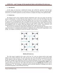
Now, after completing all the individual building blocks <strong>to</strong> design the 8-bit pipelined<br />
adder using these building blocks in the same manner. Use the 4-bit adder, 4-bit register<br />
that you have designed and FF's <strong>to</strong> complete the design as shown in Fig 1 from Lab0.<br />
Simulate the circuit by giving the appropriate inputs <strong>to</strong> verify the operation of the<br />
circuit (a subset of test cases is enough). (The output will appear at the immediate rising<br />
clock edge following the input).<br />
5. Lab Report<br />
1. Take a plot of all the schematic designs (fulladder, 4bit adder, and 8bit adder). Please clearly<br />
mention the schematic name on the plot.<br />
2. Print out the respective simulation results for all designs. The simulation must display the<br />
inputs and the corresponding outputs along with the time at which these signals are moni<strong>to</strong>red.<br />
Points will be taken off if the results are not presented clearly. Required input vec<strong>to</strong>r for<br />
each design is given below. Please initialize all inputs <strong>to</strong> zero.<br />
a. Fulladder : all available input combinations.<br />
b. 4bit adder<br />
i. 1111 + 1111 + 0 (Carry In)<br />
ii. 1010 + 1010 + 1 (Carry In)<br />
iii. 0101 + 0101 + 1 (Carry In)<br />
c. 8bit adder<br />
i. 01111110 +11100111 + 0 (Carry In)<br />
ii. 11111111 + 00000000 + 1 (Carry In)<br />
iii. 10101010 + 01010101 + 0 (Carry In)<br />
iv. 10101010 + 01010101 + 1 (Carry In)<br />
Please be cautious <strong>to</strong> clearly see when the correct outputs are generated in accordance<br />
with clock input signal. Verify this in your lab report obviously.<br />
3. Printing Tips : For schematic plot choose Design > Plot > Submit in the schematic Composer<br />
window. Click Plot Options but<strong>to</strong>n at the bot<strong>to</strong>m, and choose Plotter Name as “hpszac”, and<br />
press OK. In the Submit Plot form, click OK. It should print at the printer in 213A. For<br />
simulation results choose File > View Log File > Simulation, the simulation outputs will show<br />
Texas A & M University Page 11
<strong>ECEN</strong> <strong>454</strong> – <strong>Lab1</strong>: <strong>Introduction</strong> <strong>to</strong> <strong>Cadence</strong> <strong>Schematic</strong> <strong>Capture</strong> &<br />
Simulation<br />
up. Choose File > Save As, and put a new name on the result log file. The file is saved in your<br />
cadence direc<strong>to</strong>ry. Print out this log file using the command, “> lp –d hpszac filename”.<br />
4. Report is due by the next lab (if your lab is on Wednesday, then your due date is next<br />
Wednesday).<br />
6. <strong>Cadence</strong> Tips<br />
1. DO NOT KILL cadence process if the machine hangs. This generates view locks, which won't<br />
allow you <strong>to</strong> open the views in edit mode. Inform your TA if cadence has crashed and your<br />
standard locks would be cleared.<br />
2. Always SAVE your work. Whenever working continuously, do not wait till end <strong>to</strong> save. If<br />
cadence crashes your work will be lost.<br />
3. Please make sure you log off using “exit” when you leave since other students cannot access the<br />
machine if you do not log off and leave.<br />
Texas A & M University Page 12