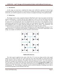
ECEN 454 â Lab1: Introduction to Cadence Schematic Capture ...
ECEN 454 â Lab1: Introduction to Cadence Schematic Capture ...
ECEN 454 â Lab1: Introduction to Cadence Schematic Capture ...

You also want an ePaper? Increase the reach of your titles
YUMPU automatically turns print PDFs into web optimized ePapers that Google loves.
<strong>ECEN</strong> <strong>454</strong> – <strong>Lab1</strong>: <strong>Introduction</strong> <strong>to</strong> <strong>Cadence</strong> <strong>Schematic</strong> <strong>Capture</strong> &<br />
Simulation<br />
Before wiring let’s see some Composer functions. You can move and copy the instances<br />
using Edit > Move and Edit > Copy functions. Also you can undo the changes made<br />
using Edit > Undo. The CIW and the lower corner of the Composer will guide you.<br />
Finally let’s wire the schematic. Choose “Add > Wire (narrow)” in the window. Click on<br />
the A pin, a wire follows you. Take it <strong>to</strong> the point you want it <strong>to</strong> go and notice that the<br />
edi<strong>to</strong>r does au<strong>to</strong>matic routing for you. Place it at the output of the proper gate. Similarly<br />
wire the rest of the circuit. Note that the wires can overlap without making contacts<br />
unless you explicitly do so. To make sure you wire <strong>to</strong> the exact place you want, notice<br />
that there is a diamond appearing when you wire <strong>to</strong> some place.<br />
You can connect up <strong>to</strong> 3 wires at one branch of wire. Pins are <strong>to</strong> be connected <strong>to</strong><br />
instances thru wires, and if you just put the Pins on the input/output pins of a gate<br />
instance, they are not actually connected. Always use wires <strong>to</strong> make connections<br />
between instances.<br />
Wire the rest of the circuit on your own. To save the design click on Design > Check and<br />
Save. Look in the icfb for error messages. If there were errors, there would also be cross<br />
markers blinking on the schematic window. Try <strong>to</strong> correct the errors and ask your TA if<br />
you need help.<br />
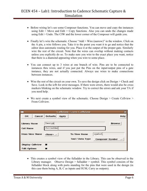
We next create a symbol view of the schematic. Choose Design > Create Cellview ><br />
From Cellview.<br />
This creates a symbol view of the fulladder in the Library. This can be observed in the<br />
Library manager. Observe Design > fulladder > symbol. This symbol consists of the<br />
fulladder block along with ports standing for the pins that were used in the design (in<br />
this case them being A, B, C as inputs and SUM, Carry as outputs).<br />
Texas A & M University Page 6