ECEN 454 â Lab1: Introduction to Cadence Schematic Capture ...
ECEN 454 â Lab1: Introduction to Cadence Schematic Capture ...
ECEN 454 â Lab1: Introduction to Cadence Schematic Capture ...

You also want an ePaper? Increase the reach of your titles
YUMPU automatically turns print PDFs into web optimized ePapers that Google loves.
<strong>ECEN</strong> <strong>454</strong> – <strong>Lab1</strong>: <strong>Introduction</strong> <strong>to</strong> <strong>Cadence</strong> <strong>Schematic</strong> <strong>Capture</strong> &<br />
Simulation<br />
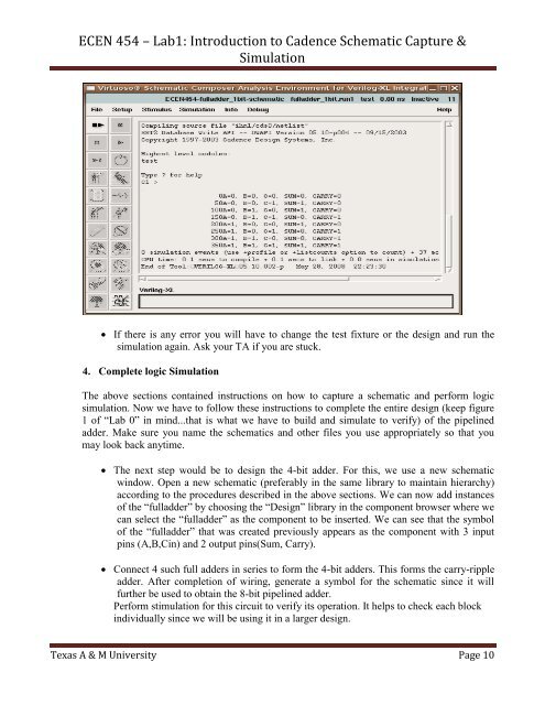
If there is any error you will have <strong>to</strong> change the test fixture or the design and run the<br />
simulation again. Ask your TA if you are stuck.<br />
4. Complete logic Simulation<br />
The above sections contained instructions on how <strong>to</strong> capture a schematic and perform logic<br />
simulation. Now we have <strong>to</strong> follow these instructions <strong>to</strong> complete the entire design (keep figure<br />
1 of “Lab 0” in mind...that is what we have <strong>to</strong> build and simulate <strong>to</strong> verify) of the pipelined<br />
adder. Make sure you name the schematics and other files you use appropriately so that you<br />
may look back anytime.<br />
The next step would be <strong>to</strong> design the 4-bit adder. For this, we use a new schematic<br />
window. Open a new schematic (preferably in the same library <strong>to</strong> maintain hierarchy)<br />
according <strong>to</strong> the procedures described in the above sections. We can now add instances<br />
of the “fulladder” by choosing the “Design” library in the component browser where we<br />
can select the “fulladder” as the component <strong>to</strong> be inserted. We can see that the symbol<br />
of the “fulladder” that was created previously appears as the component with 3 input<br />
pins (A,B,Cin) and 2 output pins(Sum, Carry).<br />
Connect 4 such full adders in series <strong>to</strong> form the 4-bit adders. This forms the carry-ripple<br />
adder. After completion of wiring, generate a symbol for the schematic since it will<br />
further be used <strong>to</strong> obtain the 8-bit pipelined adder.<br />
Perform stimulation for this circuit <strong>to</strong> verify its operation. It helps <strong>to</strong> check each block<br />
individually since we will be using it in a larger design.<br />
Texas A & M University Page 10