ECEN 454 â Lab1: Introduction to Cadence Schematic Capture ...
ECEN 454 â Lab1: Introduction to Cadence Schematic Capture ...
ECEN 454 â Lab1: Introduction to Cadence Schematic Capture ...

You also want an ePaper? Increase the reach of your titles
YUMPU automatically turns print PDFs into web optimized ePapers that Google loves.
<strong>ECEN</strong> <strong>454</strong> – <strong>Lab1</strong>: <strong>Introduction</strong> <strong>to</strong> <strong>Cadence</strong> <strong>Schematic</strong> <strong>Capture</strong> &<br />
Simulation<br />
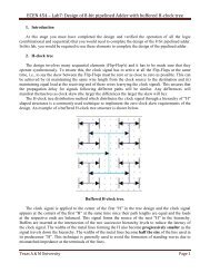
students and it also means you have <strong>to</strong> implement only the XOR and NAND2 layouts.<br />
(Remember: step 2 in section 2 of Lab0 will ask you <strong>to</strong> implement layouts of all the logic gates<br />
you used in the schematic design. Not only will you have <strong>to</strong> design fewer layouts (NAND2 instead<br />
of AND and OR) but also the implementation of a NAND2 layout can be easier than that of an<br />
AND or OR layout as you will find in the following weeks).<br />
Also, try <strong>to</strong> minimize the number of gates used in your design. A fulladder circuit can be<br />
composed of <strong>to</strong>tally 5 gates of XOR and NAND2.<br />
Place as many instances of this gate as required. When you finish press ESC key. If you<br />
have placed some extra instances then go <strong>to</strong> Edit > Delete in the Composer menu and<br />
click on the instance <strong>to</strong> delete. To exit from the Delete mode press ESC. To save the<br />
design click on Design > Save. Always save your work when you finish some important<br />
operations. When completing design, click Design > Check and Save option <strong>to</strong> verify it.<br />
Place instances of all the gates required and make you familiar with Add Instance and<br />
Delete Instance functions. Make sure you have plenty of space left for wiring your<br />
schematic. You can Zoom In and out <strong>to</strong> fit a part or whole of your design using<br />
Window → Zoom → Zoom In and Zoom Out respectively.<br />
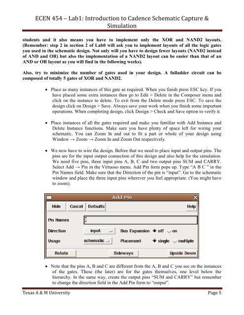
We now have <strong>to</strong> wire the design. Before that we need <strong>to</strong> place input and output pins. The<br />
pins are for the input output connection of this design and also help for the simulation.<br />
We need five pins, three input pins A, B, C and two output pins SUM and CARRY.<br />
Select Add → Pin in the Virtuoso menu. Add Pin form pops up. Type “A B C ” in the<br />
Pin Names field. Make sure that the Direction of the pin is “input”. Go <strong>to</strong> the schematic<br />
window and place the three input pins wherever you feel appropriate. (You might have<br />
<strong>to</strong> zoom).<br />
Note that the pins A, B and C are different from the A, B and C you see on the instances<br />
of the gates. These (the later) are for the gates themselves, one level below the<br />
hierarchy. In the same way, create the output pins “SUM and CARRY” but remember<br />
<strong>to</strong> change the direction field in the Add Pin form <strong>to</strong> “output”.<br />
Texas A & M University Page 5