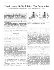
ECEN 454 Digital Integrated Circuit Design Lab9
ECEN 454 Digital Integrated Circuit Design Lab9
ECEN 454 Digital Integrated Circuit Design Lab9
- No tags were found...

Create successful ePaper yourself
Turn your PDF publications into a flip-book with our unique Google optimized e-Paper software.
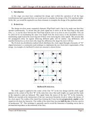
Detail procedures:a) Analyze the bottom-level subdesigns in Fig 1.Select “File->Analyze”. The Analyze File window appears. Change to the verilog directory.Select ALARM_COUNTER.v using the left mouse button.Select the remaining designs using the middle mouse button. The remaining designs include:ALARM_STATE_MACHINE.vTIME_COUNTER.vHOURS_FILTER.vTIME_STATE_MACHINE.vClick Ok.b) Elaborate each bottom-level subdesign separately.Select “File->Elaborate”. The Elaborate <strong>Design</strong> window appears. Choose the work library inthe Library list.Verify that Re-Analyze Out-Of-Date Libraries is set to on.Select the ALARM_COUNTER in the <strong>Design</strong> list.Click Ok.Elaborate the other 4 bottom subdesigns individually by repeating the above steps.c) Read in the CONVERTR block.Select “File->Read”. Change to the verilog directory.Select CONVERTOR.pla file.d) Load the subdesigns in next hierarchy level.ALARM_BLOCK.v ALARM_SM_2.v COMPARATOR.vCONVERTOR_CKT.v TIME_BLOCK.v MUX.vThe six subdesigns are all in verilog format. Use Analyze and elaborate.e) Load the Top level design.Use Analyze and elaborate to load TOP.v.f) Save the design and your attribute settingsSelect TOP designSelect “File->Save As”.
Change to your tutorial/db/ directory.Enter TOP_attributes.db in the File Name field to save the file to db directory.Check the Save All <strong>Design</strong>s in Hierarchy option.Till now, the entire design hierarchy is loaded and the designs view displays the 13 icons for thealarm clock design. Note that always save your design work in case your machine is down.2. Set attributes for the designAttributes are values set on a design that control or affect the optimization of the design. Forexample, attributes can specify the operating environment of the design, the constraint goals ofoptimization, as well as many other design parameters.g) Select TOP design.Click the down-level-button (down arrow on the left).Click the symbol view button (the 2nd button on the left).h) Set the Drive Strength on Input PortsAssume that all input ports except CLK have drive strength 0.08. Units are determined by thetarget library.Use left mouse button to select the input port ALARM. Use the middle mouse button to selectthe other input ports, except CLK. Select “Attributes->Operating Environment->DriveStrength”. The Drive Strength window displays. Type 0.08 in the Rise field. The Same Riseand fall option is checked by default.Click Apply to set the values.Click Cancel to dismiss the Drive Strength window.Set the Drive Strength for CLK to be that of pin Z of the driver cell B4I in the target library.Select CLK.Select “Attributes->Operating Environment->Drive Strength”.Enter “drive_of (class/B4I/Z)” in the Rise field. The Same Rise and fall option is checked bydefault.Click Apply to set the values.Click Cancel to dismiss the Drive Strength window.i) Set the Load on Output Ports
Load values are used to model the capacitive load on the output ports of the constrainedmodel.SPEAK_OUT drives a load of five inverters. The load of each invertor is 1.5(load of cell IVA,pin A in the target library). So the load value for SPEAK_OUT is calculated as (1.5 * 5=7.5).Loads for DISP1 and DISP2 are 3.Select the SPEAKER_OUT port.Select “Attributes->Operating Environment->Load”.Replace the contents of the capacitive load field with load_of (class/IVA/A) * 5. Leave aspace before and after the asterisk (*).Click Apply.Click Cancel to dismiss the Load window.Repeat the above steps to set capacitance load value on DISP1 and DISP2 to be 3.j) Set the Wire LoadSelect TOP.Select “Attributes->Operating Environment->Wire Load”.Select 10x10(class). As defined in the library file, 10x10 corresponds to a die size of 1mm x1mm.Click Ok.k) Set the Operating ConditionsOperating conditions are the temperature, process and voltage in which the design operates.The target library defines operating conditions. Library vendors define default operatingconditions, which can differ from one vendor to another.Select “Attributes->Operating Environment->Operating Conditions”. The operatingconditions window appears and lists operating conditions from the target library.Select WCCOM (class) in the Operating conditions window. This is the worst-casecommercial operating condition defined in the target library.Click Ok.l) Save the design and your attribute settingsSelect “File->Save As”.Change to your tutorial/db/ directory.
Enter TOP_attributes.db in the File Name field to save the file to db directory.Check the Save All <strong>Design</strong>s in Hierarchy option.Click Ok.m) Set the Optimization GoalsThe Optimization Goals include timing, area and power that you set on a design. <strong>Design</strong>Compiler checks your optimization goals during optimization and tries to meet them whilesynthesizing the design to your technology library.Set Clock ConstraintsSelect CLK in the symbol view. Click“Attributes->Clocks->Specify”. Type 25in the Period field.Click Apply.Click Cancel to dismiss the Specify Clock window.The clock object is created on CLK. Note the small waveform symbol attached to the CLKport. Set Delay ConstraintsInput/Output delays model the external delays arriving/leaving at the input/output portsof the constrained module. In this Alarm clock design, the input delay is zero. We needto set the output delay.Select the four output ports of TOP.Select “Attributes->Operating Environment->Output Delay”.Select CLK.Enter 5 in the Max Rise and Max Fall fields.Click Apply.3. Run check_designClick Cancel to dismiss the Output delay window.a) Select “Analysis->Check <strong>Design</strong>”.b) Set Check Timing to on.c) Click Ok.
The design errors window appears.d) Click the first warning message in the design errors window.e) Click “Show”.Examine two more messages.f) Click Next in the <strong>Design</strong> Errors window to highlight the next message: Pin `T0' is connectedto logic 0. Pin T0 is selected in the schematic. <strong>Design</strong> Analyzer updates the schematic in the<strong>Design</strong> Analyzer window.g) Click Next to highlight the next message. Pin T1 is selected in the schematic.h) Zoom in (from View menu on <strong>Design</strong> Analyzer window) on the area that contains pins T0and T1. The pin names for T0 and T1 are not displayed in the schematic because pin namesare turned off by default. Schematics are composed of transparent layers, each layercontaining different information. A layer of information is visible only if it is turned on.Display Pin Names Layeri) Select “View −> Style”.j) Select pin_name_layer. Set the Visible option to On.k) Click Apply. The schematic displays pin names.l) Click Cancel to dismiss the View Style window. Continue viewing errorsm) Click Next in the <strong>Design</strong> Errors window. This message is related to the earlier threemessages examined. Warning: In design `CONVERTOR_CKT', the same net is connected tomore than one pin on submodule `U7'. (LINT-33). This message and the previous threewarning messages are issued because unconnected input ports are automatically connected tologic 0 by <strong>Design</strong> Compiler. Because these warnings do not reflect problems in the design,you can ignore them. If you're using Verilog, the net name Logic 0 is connected to T0 andT1.n) Click Next in the <strong>Design</strong> Errors window. Warning: <strong>Design</strong> `CONVERTOR' is instantiated 2times. (LINT-45) Cell `U7' in design `CONVERTOR_CKT'. This message is issued becauseCONVERTOR is referenced more than once in design CONVERTOR_CKT. Resolve themultiple instances of CONVERTOR before optimization, as shown below in resolvingmultiple design instances.o) Click Cancel to dismiss the <strong>Design</strong> Errors window.Resolve Multiple <strong>Design</strong> InstancesHierarchical designs can reference a subdesign more than once. When the samesubdesign is referenced more than once in a design, multiple instances exist in thedesign. Resolve multiple design instances before you compile.
Click up-level-button (up arrow button on the left) to return the top level.Select TOP design.Select “Edit −> Uniquify −> Hierarchy”.Save the <strong>Design</strong> and run check_design again, you can see multiple design instances errordisappear.p) Select design TOP.q) Select “File −> Save As”.r) If you are not in the db directory, change to it.s) Type TOP_before_compile.db in the File Name Field.t) Verify that Save All <strong>Design</strong>s in Hierarchy option is set to on.u)Click OK.4. Optimize the <strong>Design</strong>After setting constraints & attributes on the alarm clock design and running check_design, thedesign is ready to be optimized with the compile command. Optimizing is the step in thesynthesis process that attempts to implement a combination of library cells that meets thefunctional, area and speed requirements of the design.Detail procedure:Open the <strong>Design</strong> Optimization windowa) Return to the top level and select design Top.b) Select “Tools −> <strong>Design</strong> Optimization”.Check and set optionsc) Note the default settings. Map <strong>Design</strong> (mapping) is set to on. Map Effort is set toMedium. This is the CPU effort used to map a design. For most optimizations, thedefaults are sufficient to meet defined constraints.d) Set Verify <strong>Design</strong> to on. This checks that the new synthesized design is functionallyequivalent to the original design. Use Verify Effort value Low. This is the CPU effortused to verify the design.e) Set Allow Boundary Optimization to on.Open the Background Task window
f) Set Execute In to Background.g) Click OK. The Background Task window displays.h) In the Results Directory field, type the path name of the directory in which to store theresults. This directory must not already exist. The default value is~tutorial/compile_run.i) Click Ok. A compile_run window appears and displays the optimization activities. Thewindow name is the path name to your compile directory. By default, it is~tutorial/compile_run.Evaluate and Interpret the <strong>Design</strong>Generate reports to determine whether the design goals are met. Using <strong>Design</strong> Analyzer you canselect and generate any number of attribute and analysis reports, which send output to a report windowor a file you designate.1. Open the report windowa) Display the Symbol View of TOP.b) Select “Analysis −> Report”.2. Generate Attribute ReportsTake generating bus report as an example. The bus report lists bused ports and nets in thedesign.c)Select Bussing in the open Report window.d) Click Apply.3. Generate Analysis ReportsTake generating timing report as an example. A timing report provides timing information fordefined endpoints and constrained pins. If no endpoints or constrained pins are explicitly specified, thereport includes only timing information for the most critical path in the design.Select the timing report option.e) Click Clear Choices.f) Set Timing to on. When you set Timing to on, Set Options is enabled.g) Click Set Options in the Report window.h) In the Hierarchy Options section of the window, verify First Instance Only is set to on. Onlythe first occurrence of a submodule that is used multiple times in the hierarchy is shown.i) In the Constraint Options section of the window, set Verbose to on if it is not already set.
Constraint options Worst Violations and All Violations apply only to the constraint report. Donot use them for timing reports.j) In the Timing Report Options section of the window, keep Path Delay Type as the defaultMaximum setting.k) Select Report Points and retain the Entire Path setting. Rise or fall delay is displayed foreach point in the path. This includes the incremental delay from the driver.l) Type 3 in the Max Paths to Show field to list the three paths with the longest delay.m) Click OK.n) Click Apply in the Report window.o) The timing report appears. It lists the three most critical paths in the design.4. Trace the critical pathp) Click the line in the Report Output window that displays the first cell in the path.q) Click Show. This action selects and zooms in the register (and pin) in the Schematic View.You can click Show again to enhance the highlighting.r) Continue click Next. This action highlights the points in the path.s) When you finish following the critical path, click Cancel. Remember, you must trace the firstcritical path for step u) to z)t) Select “Analysis->Highlight->Clear” to remove the highlighting on the path in theSchematic View. Then keep the schematic window.5. Use the Schematic View for AnalysisIt is not always necessary to generate reports to obtain timing or load values. You can displaythese values by selecting a pin on the schematic and requesting its timing.u) Select pin COMPARE_IN in the Schematic View. Note that COMPARE_IN is a pin of themodule ALARM_SM_2.v) Click the right mouse button in the Schematic View and select Show Timing in the menu.The Pin Values window appears and displays timing information.w) Click Cancel in the Pin Values window.Determine the load on a net.x) Select the net connecting COMPARE_IN to the COMPARATOR block.y) Select “Analysis −> Show Net Load”.
z) Click Cancel to close the Net Load window.6. Print the schematica) Select CONVERTOR_0 in the <strong>Design</strong>s View.b)Generate the Schematic View.c) Select “View −> Full View” to fit the schematic to the view window, then select “File −>Plot” in the menu bar.d) Select Current Sheet. Current Sheet prints only the sheet shown in the schematic view.e) In the Command: field, enter the print command for your local printer. Use the command “lp-d hpszac”.f) Click OK. Note that this file is not necessary in the lab report.7. Save the optimized verilog netlist.After completion of optimization save the design in the form a verilog netlist. Use “File-->SaveAs” and choose the Verilog option and save a copy of the “Top” design in the verilog folder as“Alarm_Clock.vh”.8.Synthesis of the Cruise Control LogicNow repeat the same procedure explained above to synthesize the behavioral verilog code thatwas written for the Cruise Control Logic of a vehicle in the previous lab session. But in this case weneed to synthesize the logic with a certain specific library for 180nm technology. The synopsysdatabase format(db) file for a typical 180nm technology is put up on the website. We need to ensurethat the synthesis is performed according to this library file(see below for procedure). What this meansis that the optimization (power, timing, area etc) will be performed according to the details of thestandard cells given in this file.Note: In the following lab we will use the synthesized verilog netlist that you will generate for thecruise control logic to “Place and Route” the circuit on a die.Procedure to link the given library with the synthesis process:1.Download the "iit018_stdcells.db" file from the lab website and save a copy in the ~/tutorial folder.2.After you begin <strong>Design</strong>_Analyzer , choose "Setup-->Defaults". A window pops up.3.Fill in iit018_stdcells.db in "Link Library".4.Fill in iit018_stdcells.db in "Target Library".5.Fill in generic.sdb in the "Symbol Library"6Click Ok.Now place the verilog behavioral code of the Cruise Control Logic in the ~/tutorial/verilog folder andrepeat the same procedure as above to optimize the logic and generate the synthesized netlist.Note:1. While assigning the drive strength for the clock, the above given procedure of usingdrive_of(class/B4I/Z) will not work since the target library does not remain the same. Hence use anabsolute value of 0.03352. Use a load of 3 on the output ports.
3. Also you need not set the Wire Load in this case.4. And for operating conditions use the "typical" option provided by the library.5. Use a clock period of 25 and set the output delay to 5 in both the Max Rise and Max Fall fields.Make sure you save the synthesized netlist (after performing optimization) of the design inverilog format. This file will be required for the next lab.Report Requirements:1. Print schematics of TOP and TIME_COUNTER.2. After performing the optimization of the Cruise Control Logic, print out the schematic of eachmodule in the circuit.3.Report the most critical path in the circuit,plot it out on the schematic window (MUST highlight it).4.Report the most critical path in the circuit, send the output to a file named "report.out",print the fileout.5.Print out the final synthesized verilog netlist of the cruise control logic.