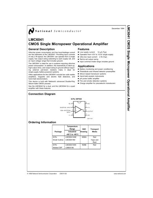
LMC6041 CMOS Single Micropower Operational Amplifier - Futurlec
LMC6041 CMOS Single Micropower Operational Amplifier - Futurlec
LMC6041 CMOS Single Micropower Operational Amplifier - Futurlec

You also want an ePaper? Increase the reach of your titles
YUMPU automatically turns print PDFs into web optimized ePapers that Google loves.
<strong>LMC6041</strong><br />
<strong>CMOS</strong> <strong>Single</strong> <strong>Micropower</strong> <strong>Operational</strong> <strong>Amplifier</strong><br />
General Description<br />
Ultra-low power consumption and low input-leakage current<br />
are the hallmarks of the <strong>LMC6041</strong>. Providing input currents<br />
of only 2 fA typical, the <strong>LMC6041</strong> can operate from a single<br />
supply, has output swing extending to each supply rail, and<br />
an input voltage range that includes ground.<br />
The <strong>LMC6041</strong> is ideal for use in systems requiring ultra-low<br />
power consumption. In addition, the insensitivity to latch-up,<br />
high output drive, and output swing to ground without requiring<br />
external pull-down resistors make it ideal for<br />
single-supply battery-powered systems.<br />
Other applications for the <strong>LMC6041</strong> include bar code reader<br />
amplifiers, magnetic and electric field detectors, and<br />
hand-held electrometers.<br />
This device is built with National’s advanced Double-Poly<br />
Silicon-Gate <strong>CMOS</strong> process.<br />
See the LMC6042 for a dual, and the LMC6044 for a quad<br />
amplifier with these features.<br />
Connection Diagram<br />
8-Pin DIP/SO<br />
Features<br />
n Low supply current: 14 µA (Typ)<br />
n Operates from 4.5V to 15.5V single supply<br />
n Ultra low input current: 2 fA (Typ)<br />
n Rail-to-rail output swing<br />
n Input common-mode range includes ground<br />
Applications<br />
n Battery monitoring and power conditioning<br />
n Photodiode and infrared detector preamplifier<br />
n Silicon based transducer systems<br />
n Hand-held analytic instruments<br />
n pH probe buffer amplifier<br />
n Fire and smoke detection systems<br />
n Charge amplifier for piezoelectric transducers<br />
December 1994<br />
<strong>LMC6041</strong> <strong>CMOS</strong> <strong>Single</strong> <strong>Micropower</strong> <strong>Operational</strong> <strong>Amplifier</strong><br />
Ordering Information<br />
Temperature<br />
Range<br />
NSC<br />
Drawing<br />
DS011136-1<br />
Transport<br />
Media<br />
Package Industrial<br />
−40˚C to +85˚C<br />
8-Pin <strong>LMC6041</strong>AIM M08A Rail<br />
Small Outline <strong>LMC6041</strong>IM Tape and<br />
Reel<br />
8-Pin <strong>LMC6041</strong>AIN N08E Rail<br />
Molded DIP LM6041IN<br />
© 1999 National Semiconductor Corporation DS011136 www.national.com
Absolute Maximum Ratings (Note 1)<br />
If Military/Aerospace specified devices are required,<br />
please contact the National Semiconductor Sales Office/<br />
Distributors for availability and specifications.<br />
Differential Input Voltage<br />
±Supply Voltage<br />
Supply Voltage (V + −V − )<br />
16V<br />
Output Short Circuit to V − (Note 2)<br />
Output Short Circuit to V + (Note 11)<br />
Lead Temperature<br />
(Soldering, 10 sec.)<br />
260˚C<br />
Storage Temperature Range<br />
−65˚C to +150˚C<br />
Junction Temperature<br />
110˚C<br />
ESD Tolerance (Note 4)<br />
500V<br />
Current at Input Pin<br />
±5 mA<br />
Current at Output Pin<br />
±18 mA<br />
Current at Power Supply Pin<br />
35 mA<br />
Voltage at Input/Output Pin (V + ) + 0.3V, (V − ) − 0.3V<br />
Power Dissipation (Note 3)<br />
Operating Ratings<br />
Temperature Range<br />
<strong>LMC6041</strong>AI, <strong>LMC6041</strong>I<br />
−40˚C ≤ T J ≤ +85˚C<br />
Supply Voltage 4.5V ≤ V + ≤ 15.5V<br />
Power Dissipation (Note 9)<br />
Thermal Resistance (θ JA ) (Note 10)<br />
8-Pin DIP<br />
101˚C/W<br />
8-Pin SO<br />
165˚C/W<br />
Electrical Characteristics<br />
Unless otherwise specified, all limits guaranteed for T A<br />
= T J<br />
= 25˚C. Boldface limits apply at the temperature extremes. V + =<br />
5V, V − = 0V, V CM<br />
= 1.5V, V O<br />
= V + /2, and R L<br />
> 1M unless otherwise specified.<br />
Typical <strong>LMC6041</strong>AI <strong>LMC6041</strong>I Units<br />
Symbol Parameter Conditions (Note 5) Limit Limit (Limit)<br />
(Note 6) (Note 6)<br />
V OS Input Offset Voltage 1 3 6 mV<br />
3.3 6.3 max<br />
TCV OS Input Offset Voltage 1.3 µV/˚C<br />
Average Drift<br />
I B Input Bias Current 0.002 4 4 pA<br />
max<br />
I OS Input Offset Current 0.001 2 2 pA<br />
max<br />
R IN Input Resistance >10 TeraΩ<br />
CMRR Common Mode 0V ≤ V CM ≤ 12.0V 75 68 62 dB<br />
Rejection Ratio V + = 15V 66 60 min<br />
+PSRR Positive Power Supply 5V ≤ V + ≤ 15V 75 68 62 dB<br />
Rejection Ratio V O<br />
= 2.5V 66 60 min<br />
−PSRR Negative Power Supply 0V ≤ V − ≤ −10V 94 84 74 dB<br />
Rejection Ratio V O<br />
= 2.5V 83 73 min<br />
CMR Input Common-Mode V + = 5V and 15V −0.4 −0.1 −0.1 V<br />
Voltage Range for CMRR ≥ 50 dB 0 0 max<br />
V + − 1.9V V + − 2.3V V + − 2.3V V<br />
V + − 2.5V V + − 2.4V min<br />
A V Large Signal R L<br />
= 100 kΩ (Note 7) Sourcing 1000 400 300 V/mV<br />
Voltage Gain 300 200 min<br />
Sinking 500 180 90 V/mV<br />
120 70 min<br />
R L<br />
= 25 kΩ (Note 7) Sourcing 1000 200 100 V/mV<br />
160 80 min<br />
Sinking 250 100 50 V/mV<br />
60 40 min<br />
www.national.com 2
Electrical Characteristics (Continued)<br />
Unless otherwise specified, all limits guaranteed for T A<br />
= T J<br />
= 25˚C. Boldface limits apply at the temperature extremes. V + =<br />
5V, V − = 0V, V CM<br />
= 1.5V, V O<br />
= V + /2, and R L<br />
> 1M unless otherwise specified.<br />
Typical <strong>LMC6041</strong>AI <strong>LMC6041</strong>I Units<br />
Symbol Parameter Conditions (Note 5) Limit Limit (Limit)<br />
(Note 6) (Note 6)<br />
V O Output Swing V + = 5V 4.987 4.970 4.940 V<br />
R L<br />
= 100 kΩ to V + /2 4.950 4.910 min<br />
0.004 0.030 0.060 V<br />
0.050 0.090 max<br />
V + = 5V 4.980 4.920 4.870 V<br />
R L<br />
= 25 kΩ to V + /2 4.870 4.820 min<br />
0.010 0.080 0.130 V<br />
0.130 0.180 max<br />
V + = 15V 14.970 14.920 14.880 V<br />
R L<br />
= 100 kΩ to V + /2 14.880 14.820 min<br />
0.007 0.030 0.060 V<br />
0.050 0.090 max<br />
V + = 15V 14.950 14.900 14.850 V<br />
R L<br />
= 25 kΩ to V + /2 14.850 14.800 min<br />
0.022 0.100 0.150 V<br />
0.150 0.200 max<br />
I SC Output Current Sourcing, V O<br />
= 0V 22 16 13 mA<br />
V + = 5V 10 8 min<br />
Sinking, V O<br />
= 5V 21 16 13 mA<br />
8 8 min<br />
I SC Output Current Sourcing, V O<br />
= 0V 40 15 15 mA<br />
V + = 15V 10 10 min<br />
Sinking, V O<br />
= 13V 39 24 21 mA<br />
(Note 11) 8 8 min<br />
I S Supply Current V O<br />
= 1.5V 14 20 26 µA<br />
24 30 max<br />
V + = 15V 18 26 34 µA<br />
31 39 max<br />
AC Electrical Characteristics<br />
Unless otherwise specified, all limits guaranteed for T A<br />
= T J<br />
= 25˚C. Boldface limits apply at the temperature extremes. V + =<br />
5V, V − = 0V, V CM<br />
= 1.5V, V O<br />
= V + /2, and R L<br />
> 1M unless otherwise specified.<br />
Typ <strong>LMC6041</strong>AI <strong>LMC6041</strong>I Units<br />
Symbol Parameter Conditions (Note 5) Limit Limit (Limit)<br />
(Note 6) (Note 6)<br />
SR Slew Rate (Note 8) 0.02 0.015 0.010 V/µs<br />
0.010 0.007 min<br />
GBW Gain-Bandwidth Product 75 kHz<br />
φ m Phase Margin 60 Deg<br />
e n Input-Referred F = 1 kHz 83 nV/√Hz<br />
Voltage Noise<br />
i n Input-Referred F = 1 kHz 0.0002 pA/√Hz<br />
Current Noise<br />
T.H.D. Total Harmonic F = 1 kHz, A V<br />
= −5<br />
Distortion R L<br />
= 100 kΩ, V O<br />
=2V pp 0.01 %<br />
±5V Supply<br />
3<br />
www.national.com
AC Electrical Characteristics (Continued)<br />
Note 1: Absolute Maximum Ratings indicate limits beyond which damage to the device may occur. Operating conditions indicate conditions for which the device is<br />
intended to be functional, but do not guarantee specific performance limits. For guaranteed specifications and test conditions, see the Electrical Characteristics. The<br />
guaranteed specifications apply only for the test conditions listed.<br />
Note 2: Applies to both single-supply and split-supply operation. Continuous short circuit operation at elevated ambient temperature can result in exceeding the<br />
maximum allowed junction temperature of 110˚C. Output currents in excess of ±30 mA over long term may adversely affect reliability.<br />
Note 3: The maximum power dissipation is a function of T J(max) , θ JA , and T A . The maximum allowable power dissipation at any ambient temperature is P D = (T J(max)<br />
−T A )/θ JA .<br />
Note 4: Human body model, 1.5 kΩ in series with 100 pF.<br />
Note 5: Typical Values represent the most likely parametric norm.<br />
Note 6: All limits are guaranteed at room temperature (standard type face) or at operating temperature extremes (bold face type).<br />
Note 7: V + = 15V, V CM = 7.5V and R L connected to 7.5V. For Sourcing tests, 7.5V ≤ V O ≤ 11.5V. For Sinking tests, 2.5V ≤ V O ≤ 7.5V.<br />
Note 8: V + = 15V. Connected as Voltage Follower with 10V step input. Number specified in the slower of the positive and negative slew rates.<br />
Note 9: For operating at elevated temperatures the device must be derated based on the thermal resistance θ JA with P D = (T J −T A )/θ JA .<br />
Note 10: All numbers apply for packages soldered directly into a PC board.<br />
Note 11: Do not connect output to V + when V + is greater than 13V or reliability may be adversely affected.<br />
Typical Performance Characteristics V S<br />
= ± 7.5V, T A<br />
= 25˚C unless otherwise specified<br />
Supply Current vs<br />
Supply Voltage<br />
Offset Voltage vs<br />
Temperature of Five<br />
Representative Units<br />
Input Bias Current<br />
vs Temperature<br />
DS011136-19<br />
DS011136-21<br />
DS011136-20<br />
Input Bias Current<br />
vs Input Common-Mode<br />
Voltage<br />
Input Common-Mode<br />
Voltage Range vs<br />
Temperature<br />
Output Characteristics<br />
Current Sinking<br />
DS011136-22<br />
DS011136-23<br />
DS011136-24<br />
www.national.com 4
Typical Performance Characteristics V S<br />
= ± 7.5V, T A<br />
= 25˚C unless otherwise<br />
specified (Continued)<br />
Output Characteristics<br />
Current Sourcing<br />
Input Voltage Noise<br />
vs Frequency<br />
Power Supply Rejection<br />
Ratio vs Frequency<br />
DS011136-25<br />
DS011136-26<br />
DS011136-27<br />
CMRR vs Frequency<br />
CMRR vs Temperature<br />
Open-Loop Voltage Gain<br />
vs Temperature<br />
DS011136-28<br />
DS011136-29<br />
DS011136-30<br />
Open-Loop<br />
Frequency Response<br />
Gain and Phase<br />
Responses vs<br />
Load Capacitance<br />
Gain and Phase<br />
Responses vs<br />
Temperature<br />
DS011136-31<br />
DS011136-32<br />
DS011136-33<br />
5<br />
www.national.com
Typical Performance Characteristics V S<br />
= ± 7.5V, T A<br />
= 25˚C unless otherwise<br />
specified (Continued)<br />
Gain Error<br />
(V OS vs V OUT )<br />
Common-Mode Error vs<br />
Common-Mode Voltage of<br />
Three Representative Units<br />
Non-Inverting<br />
Slew Rate<br />
vs Temperature<br />
DS011136-34<br />
DS011136-35<br />
DS011136-36<br />
Inverting Slew Rate<br />
vs Temperature<br />
Non-Inverting Large<br />
Signal Pulse Response<br />
(A V<br />
= +1)<br />
Non-Inverting Small<br />
Signal Pulse Response<br />
DS011136-37<br />
DS011136-38<br />
DS011136-39<br />
Inverting Large-Signal<br />
Pulse Response<br />
Inverting Small Signal<br />
Pulse Response<br />
Stability vs<br />
Capacitive Load<br />
(A V<br />
= +1)<br />
DS011136-40<br />
DS011136-41<br />
DS011136-42<br />
www.national.com 6
Typical Performance Characteristics V S<br />
= ± 7.5V, T A<br />
= 25˚C unless otherwise<br />
specified (Continued)<br />
Stability vs<br />
Capacitive Load<br />
(A V<br />
= ±10)<br />
DS011136-43<br />
Applications Hints<br />
AMPLIFIER TOPOLOGY<br />
The <strong>LMC6041</strong> incorporates a novel op-amp design topology<br />
that enables it to maintain rail-to-rail output swing even when<br />
driving a large load. Instead of relying on a push-pull unity<br />
gain output buffer stage, the output stage is taken directly<br />
from the internal integrator, which provides both low output<br />
impedance and large gain. Special feed-forward compensation<br />
design techniques are incorporated to maintain stability<br />
over a wider range of operating conditions than traditional<br />
micropower op-amps. These features make the <strong>LMC6041</strong><br />
both easier to design with, and provide higher speed than<br />
products typically found in this ultra-low power class.<br />
COMPENSATING FOR INPUT CAPACITANCE<br />
It is quite common to use large values of feedback resistance<br />
with amplifiers with ultra-low input current, like the<br />
<strong>LMC6041</strong>.<br />
Although the <strong>LMC6041</strong> is highly stable over a wide range of<br />
operating conditions, certain precautions must be met to<br />
achieve the desired pulse response when a large feedback<br />
resistor is used. Large feedback resistors and even small<br />
values of input capacitance, due to transducers, photodiodes,<br />
and circuits board parasitics, reduce phase margins.<br />
When high input impedance are demanded, guarding of the<br />
<strong>LMC6041</strong> is suggested. Guarding input lines will not only reduce<br />
leakage, but lowers stray input capacitance as well.<br />
(See Printed-Circuit-Board Layout for High Impedance<br />
Work.)<br />
The effect of input capacitance can be compensated for by<br />
adding a capacitor. Adding a capacitor, C f , around the feedback<br />
resistor (as in Figure 1 ) such that:<br />
or<br />
R 1 C IN ≤ R 2 C f<br />
Since it is often difficult to know the exact value of C IN ,C f can<br />
be experimentally adjusted so that the desired pulse response<br />
is achieved. Refer to the LMC660 and the LMC662<br />
for a more detailed discussion on compensating for input capacitance.<br />
CAPACITIVE LOAD TOLERANCE<br />
Direct capacitive loading will reduce the phase margin of<br />
many op-amps. A pole in the feedback loop is created by the<br />
combination of the op-amp’s output impedance and the capacitive<br />
load. This pole induces phase lag at the unity-gain<br />
crossover frequency of the amplifier resulting in either an oscillatory<br />
or underdamped pulse response. With a few external<br />
components, op amps can easily indirectly drive capacitive<br />
loads, as shown in Figure 2.<br />
DS011136-5<br />
FIGURE 1. Cancelling the Effect of Input Capacitance<br />
7<br />
www.national.com
Applications Hints (Continued)<br />
PRINTED-CIRCUIT-BOARD LAYOUT<br />
FOR HIGH-IMPEDANCE WORK<br />
It is generally recognized that any circuit which must operate<br />
with less than 1000 pA of leakage current requires special<br />
layout of the PC board. When one wishes to take advantage<br />
of the ultra-low bias current of the <strong>LMC6041</strong>, typically less<br />
than 2fA, it is essential to have an excellent layout. Fortunately,<br />
the techniques of obtaining low leakages are quite<br />
simple. First, the user must not ignore the surface leakage of<br />
the PC board, even though it may sometimes appear acceptably<br />
low, because under conditions of high humidity or dust<br />
or contamination, the surface leakage will be appreciable.<br />
To minimize the effect of any surface leakage, lay out a ring<br />
of foil completely surrounding the <strong>LMC6041</strong>’s inputs and the<br />
terminals of capacitors, diodes, conductors, resistors, relay<br />
terminals, etc. connected to the op-amp’s inputs, as in Figure<br />
4. To have a significant effect, guard rings should be<br />
placed on both the top and bottom of the PC board. This PC<br />
foil must then be connected to a voltage which is at the same<br />
voltage as the amplifer inputs, since no leakage current can<br />
flow between two points at the same potential. For example,<br />
a PC board trace-to-pad resistance of 10 12 Ω, which is normally<br />
considered a very large resistance, could leak 5 pA if<br />
the trace were a 5V bus adjacent to the pad of the input. This<br />
would cause a 100 times degradation from the <strong>LMC6041</strong>’s<br />
actual performance. However, if a guard ring is held within 5<br />
mV of the inputs, then even a resistance of 10 11 Ω would<br />
cause only 0.05 pA of leakage current. See Figure 5 for typical<br />
connections of guard rings for standard op-amp<br />
configurations.<br />
DS011136-6<br />
FIGURE 2. <strong>LMC6041</strong> Noninverting Gain of 10 <strong>Amplifier</strong>,<br />
Compensated to Handle Capacitive Loads<br />
In the circuit of Figure 2, R1 and C1 serve to counteract the<br />
loss of phase margin by feeding the high frequency component<br />
of the output signal back to the amplifier’s inverting input,<br />
thereby preserving phase margin in the overall feedback<br />
loop.<br />
Capacitive load driving capability is enhanced by using a pull<br />
up resistor to V + (Figure 3 ). Typically a pull up resistor conducting<br />
10 µA or more will significantly improve capacitive<br />
load responses. The value of the pull up resistor must be determined<br />
based on the current sinking capability of the amplifier<br />
with respect to the desired output swing. Open loop gain<br />
of the amplifier can also be affected by the pull up resistor<br />
(see Electrical Characteristics).<br />
FIGURE 4. Example of Guard Ring<br />
in P.C. Board Layout<br />
DS011136-7<br />
DS011136-18<br />
FIGURE 3. Compensating for Large<br />
Capacitive Loads with a Pull Up Resistor<br />
www.national.com 8
Applications Hints (Continued)<br />
Typical <strong>Single</strong>-Supply Applications<br />
(V + = 5.0 V DC )<br />
The extremely high input impedance, and low power consumption,<br />
of the <strong>LMC6041</strong> make it ideal for applications that<br />
require battery-powered instrumentation amplifiers. Examples<br />
of these type of applications are hand-held pH<br />
probes, analytic medical instruments, magnetic field detectors,<br />
gas detectors, and silicon based pressure transducers.<br />
Inverting <strong>Amplifier</strong><br />
DS011136-8<br />
DS011136-12<br />
FIGURE 7. Two Op-Amp Instrumentation <strong>Amplifier</strong><br />
Follower<br />
DS011136-9<br />
DS011136-10<br />
Non-Inverting <strong>Amplifier</strong><br />
FIGURE 5. Typical Connections of Guard Rings<br />
The designer should be aware that when it is inappropriate<br />
to lay out a PC board for the sake of just a few circuits, there<br />
is another technique which is even better than a guard ring<br />
on a PC board: Don’t insert the amplifier’s input pin into the<br />
board at all, but bend it up in the air and use only air as an insulator.<br />
Air is an excellent insulator. In this case you may<br />
have to forego some of the advantages of PC board construction,<br />
but the advantages are sometimes well worth the<br />
effort of using point-to-point up-in-the-air wiring. See Figure<br />
6.<br />
The circuit in Figure 7 is recommended for applications<br />
where the common-mode input range is relatively low and<br />
the differential gain will be in the range of 10 to 1000. This<br />
two op-amp instrumentation amplifier features an independent<br />
adjustment of the gain and common-mode rejection<br />
trim, and a total quiescent supply current of less than 28 µA.<br />
To maintain ultra-high input impedance, it is advisable to use<br />
ground rings and consider PC board layout an important part<br />
of the overall system design (see Printed-Circuit-Board Layout<br />
for High Impedance Work). Referring to Figure 7, the input<br />
voltages are represented as a common-mode input V CM<br />
plus a differential input V D .<br />
Rejection of the common-mode component of the input is<br />
accomplished by making the ratio of R1/R2 equal to R3/R4.<br />
So that where,<br />
A suggested design guideline is to minimize the difference of<br />
value between R1 through R4. This will often result in improved<br />
resistor tempco, amplifier gain, and CMRR over temperature.<br />
If RN = R1 = R2 = R3 = R4 then the gain equation<br />
can be simplified:<br />
DS011136-11<br />
(Input pins are lifted out of PC board and soldered directly to components.<br />
All other pins connected to PC board.)<br />
FIGURE 6. Air Wiring<br />
Due to the “zero-in, zero-out” performance of the <strong>LMC6041</strong>,<br />
and output swing rail-rail, the dynamic range is only limited to<br />
the input common-mode range of 0V to V S –2.3V, worst case<br />
at room temperature. This feature of the <strong>LMC6041</strong> makes it<br />
an ideal choice for low-power instrumentation systems.<br />
A complete instrumentation amplifier designed for a gain of<br />
100 is shown in Figure 8. Provisions have been made for low<br />
sensitivity trimming of CMRR and gain.<br />
9<br />
www.national.com
Typical <strong>Single</strong>-Supply Applications (V + = 5.0 V DC ) (Continued)<br />
FIGURE 8. Low-Power Two-Op-Amp Instrumentation <strong>Amplifier</strong><br />
DS011136-13<br />
DS011136-14<br />
FIGURE 9. Low-Leakage Sample and Hold<br />
DS011136-16<br />
FIGURE 11. 1 Hz Square-Wave Oscillator<br />
FIGURE 10. Instrumentation <strong>Amplifier</strong><br />
DS011136-15<br />
DS011136-17<br />
FIGURE 12. AC Coupled Power <strong>Amplifier</strong><br />
www.national.com 10
Physical Dimensions inches (millimeters) unless otherwise noted<br />
8-Pin Small Outline<br />
Order Number <strong>LMC6041</strong>AIM or <strong>LMC6041</strong>IM<br />
NS Package Number M08A<br />
8-Pin Molded DIP<br />
Order Number <strong>LMC6041</strong>AIN or <strong>LMC6041</strong>IN<br />
NS Package Number N08E<br />
11<br />
www.national.com
<strong>LMC6041</strong> <strong>CMOS</strong> <strong>Single</strong> <strong>Micropower</strong> <strong>Operational</strong> <strong>Amplifier</strong><br />
Notes<br />
LIFE SUPPORT POLICY<br />
NATIONAL’S PRODUCTS ARE NOT AUTHORIZED FOR USE AS CRITICAL COMPONENTS IN LIFE SUPPORT<br />
DEVICES OR SYSTEMS WITHOUT THE EXPRESS WRITTEN APPROVAL OF THE PRESIDENT OF NATIONAL<br />
SEMICONDUCTOR CORPORATION. As used herein:<br />
1. Life support devices or systems are devices or<br />
systems which, (a) are intended for surgical implant<br />
into the body, or (b) support or sustain life, and<br />
whose failure to perform when properly used in<br />
accordance with instructions for use provided in the<br />
labeling, can be reasonably expected to result in a<br />
significant injury to the user.<br />
2. A critical component is any component of a life<br />
support device or system whose failure to perform<br />
can be reasonably expected to cause the failure of<br />
the life support device or system, or to affect its<br />
safety or effectiveness.<br />
National Semiconductor<br />
Corporation<br />
Americas<br />
Tel: 1-800-272-9959<br />
Fax: 1-800-737-7018<br />
Email: support@nsc.com<br />
www.national.com<br />
National Semiconductor<br />
Europe<br />
Fax: +49 (0) 1 80-530 85 86<br />
Email: europe.support@nsc.com<br />
Deutsch Tel: +49 (0) 1 80-530 85 85<br />
English Tel: +49 (0) 1 80-532 78 32<br />
Français Tel: +49 (0) 1 80-532 93 58<br />
Italiano Tel: +49 (0) 1 80-534 16 80<br />
National Semiconductor<br />
Asia Pacific Customer<br />
Response Group<br />
Tel: 65-2544466<br />
Fax: 65-2504466<br />
Email: sea.support@nsc.com<br />
National Semiconductor<br />
Japan Ltd.<br />
Tel: 81-3-5639-7560<br />
Fax: 81-3-5639-7507<br />
National does not assume any responsibility for use of any circuitry described, no circuit patent licenses are implied and National reserves the right at any time without notice to change said circuitry and specifications.