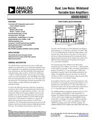
LMC6034 CMOS Quad Operational Amplifier - Futurlec
LMC6034 CMOS Quad Operational Amplifier - Futurlec
LMC6034 CMOS Quad Operational Amplifier - Futurlec

Create successful ePaper yourself
Turn your PDF publications into a flip-book with our unique Google optimized e-Paper software.
<strong>LMC6034</strong><br />
<strong>CMOS</strong> <strong>Quad</strong> <strong>Operational</strong> <strong>Amplifier</strong><br />
General Description<br />
The <strong>LMC6034</strong> is a <strong>CMOS</strong> quad operational amplifier which<br />
can operate from either a single supply or dual supplies. Its<br />
performance features include an input common-mode range<br />
that reaches ground, low input bias current, and high voltage<br />
gain into realistic loads, such as 2 kΩ and 600Ω.<br />
This chip is built with National’s advanced Double-Poly<br />
Silicon-Gate <strong>CMOS</strong> process.<br />
See the LMC6032 datasheet for a <strong>CMOS</strong> dual operational<br />
amplifier with these same features. For higher performance<br />
characteristics refer to the LMC660.<br />
Features<br />
n Specified for 2 kΩ and 600Ω loads<br />
n High voltage gain: 126 dB<br />
Connection Diagram<br />
14-Pin DIP/SO<br />
n Low offset voltage drift: 2.3 µV/˚C<br />
n Ultra low input bias current: 40 fA<br />
n Input common-mode range includes V −<br />
n Operating Range from +5V to +15V supply<br />
n I SS<br />
= 400 µA/amplifier; independent of V +<br />
n Low distortion: 0.01% at 10 kHz<br />
n Slew rate: 1.1 V/µs<br />
n Improved performance over TLC274<br />
Applications<br />
n High-impedance buffer or preamplifier<br />
n Current-to-voltage converter<br />
n Long-term integrator<br />
n Sample-and-hold circuit<br />
n Medical instrumentation<br />
May 1998<br />
<strong>LMC6034</strong> <strong>CMOS</strong> <strong>Quad</strong> <strong>Operational</strong> <strong>Amplifier</strong><br />
Ordering Information<br />
Top View<br />
DS011134-1<br />
Temperature Range Package NSC Transport<br />
Industrial<br />
−40˚C ≤ T J ≤ +85˚C<br />
<strong>LMC6034</strong>IN 14-Pin<br />
Drawing<br />
N14A<br />
Media<br />
Rail<br />
Molded DIP<br />
<strong>LMC6034</strong>IM 14-Pin M14A Rail<br />
Small Outline<br />
Tape and Reel<br />
© 1999 National Semiconductor Corporation DS011134 www.national.com
Absolute Maximum Ratings (Note 1)<br />
If Military/Aerospace specified devices are required,<br />
please contact the National Semiconductor Sales Office/<br />
Distributors for availability and specifications.<br />
Differential Input Voltage<br />
±Supply Voltage<br />
Supply Voltage (V + −V − )<br />
16V<br />
Output Short Circuit to V + (Note 10)<br />
Output Short Circuit to V − (Note 2)<br />
Lead Temperature<br />
(Soldering, 10 sec.)<br />
260˚C<br />
Storage Temperature Range<br />
−65˚C to +150˚C<br />
Power Dissipation (Note 3)<br />
Voltage at Output/Input Pin (V + ) +0.3V, (V − ) −0.3V<br />
Current at Output Pin<br />
±18 mA<br />
Current at Input Pin<br />
Current at Power Supply Pin<br />
Junction Temperature (Note 3)<br />
ESD Tolerance (Note 4)<br />
Operating Ratings(Note 1)<br />
±5 mA<br />
35 mA<br />
150˚C<br />
1000V<br />
Temperature Range<br />
−40˚C ≤ T J ≤ +85˚C<br />
Supply Voltage Range 4.75V to 15.5V<br />
Power Dissipation (Note 11)<br />
Thermal Resistance (θ JA ), (Note 12)<br />
14-Pin DIP<br />
85˚C/W<br />
14-Pin SO<br />
115˚C/W<br />
DC Electrical Characteristics<br />
Unless otherwise specified, all limits guaranteed for T J<br />
= 25˚C. Boldface limits apply at the temperature extremes. V + = 5V,<br />
V − = GND = 0V, V CM<br />
= 1.5V, V OUT<br />
= 2.5V, and R L<br />
> 1M unless otherwise specified.<br />
Symbol Parameter Conditions Typical <strong>LMC6034</strong>I Units<br />
(Note 5)<br />
Limit<br />
(Note 6)<br />
V OS Input Offset Voltage 1 9 mV<br />
11 max<br />
∆V OS /∆T Input Offset Voltage 2.3 µV/˚C<br />
Average Drift<br />
I B Input Bias Current 0.04 pA<br />
200 max<br />
I OS Input Offset Current 0.01 pA<br />
100 max<br />
R IN Input Resistance >1 TeraΩ<br />
CMRR Common Mode 0V ≤ V CM ≤ 12V 83 63 dB<br />
Rejection Ratio V + = 15V 60 min<br />
+PSRR Positive Power Supply 5V ≤ V + ≤ 15V 83 63 dB<br />
Rejection Ratio V O<br />
= 2.5V 60 min<br />
−PSRR Negative Power Supply 0V ≤ V − ≤ −10V 94 74 dB<br />
Rejection Ratio 70 min<br />
V CM Input Common-Mode V + = 5V & 15V −0.4 −0.1 V<br />
Voltage Range For CMRR ≥ 50 dB 0 max<br />
V + − 1.9 V + − 2.3 V<br />
V + − 2.6 min<br />
A V Large Signal Voltage Gain R L<br />
= 2kΩ(Note 7) 2000 200 V/mV<br />
Sourcing 100 min<br />
Sinking 500 90 V/mV<br />
40 min<br />
R L<br />
= 600Ω (Note 7) 1000 100 V/mV<br />
Sourcing 75 min<br />
Sinking 250 50 V/mV<br />
20 min<br />
www.national.com 2
DC Electrical Characteristics (Continued)<br />
Unless otherwise specified, all limits guaranteed for T J<br />
= 25˚C. Boldface limits apply at the temperature extremes. V + = 5V,<br />
V − = GND = 0V, V CM<br />
= 1.5V, V OUT<br />
= 2.5V, and R L<br />
> 1M unless otherwise specified.<br />
Symbol Parameter Conditions Typical <strong>LMC6034</strong>I Units<br />
(Note 5)<br />
Limit<br />
(Note 6)<br />
V O Output Voltage Swing V + = 5V 4.87 4.20 V<br />
R L<br />
= 2kΩto 2.5V 4.00 min<br />
0.10 0.25 V<br />
0.35 max<br />
V + = 5V 4.61 4.00 V<br />
R L<br />
= 600Ω to 2.5V 3.80 min<br />
0.30 0.63 V<br />
0.75 max<br />
V + = 15V 14.63 13.50 V<br />
R L<br />
= 2kΩto 7.5V 13.00 min<br />
0.26 0.45 V<br />
0.55 max<br />
V + = 15V 13.90 12.50 V<br />
R L<br />
= 600Ω to 7.5V 12.00 min<br />
0.79 1.45 V<br />
1.75 max<br />
I O Output Current V + = 5V 22 13 mA<br />
Sourcing, V O<br />
= 0V 9 min<br />
Sinking, V O<br />
= 5V 21 13 mA<br />
9 min<br />
V + = 15V 40 23 mA<br />
Sourcing, V O<br />
= 0V 15 min<br />
Sinking, V O<br />
= 13V 39 23 mA<br />
(Note 10) 15 min<br />
I S Supply Current All Four <strong>Amplifier</strong>s 1.5 2.7 mA<br />
V O<br />
= 1.5V 3.0 max<br />
3<br />
www.national.com
AC Electrical Characteristics<br />
Unless otherwise specified, all limits guaranteed for T J<br />
= 25˚C. Boldface limits apply at the temperature extremes. V + = 5V,<br />
V − = GND = 0V, V CM<br />
= 1.5V, V OUT<br />
= 2.5V, and R L<br />
> 1M unless otherwise specified.<br />
Symbol Parameter Conditions Typical <strong>LMC6034</strong>I Units<br />
(Note 5)<br />
Limit<br />
(Note 6)<br />
SR Slew Rate (Note 8) 1.1 0.8 V/µs<br />
0.4 min<br />
GBW Gain-Bandwidth Product 1.4 MHz<br />
φ M Phase Margin 50 Deg<br />
G M Gain Margin 17 dB<br />
Amp-to-Amp Isolation (Note 9) 130 dB<br />
e n Input-Referred Voltage Noise F = 1 kHz 22<br />
i n Input-Referred Current Noise F = 1 kHz 0.0002<br />
THD Total Harmonic Distortion F = 10 kHz, A V<br />
= −10<br />
R L<br />
= 2kΩ,V O<br />
=8V PP 0.01 %<br />
±5V Supply<br />
Note 1: Absolute Maximum Ratings indicate limits beyond which damage to the component may occur. Operating Ratings indicate conditions for which the device<br />
is intended to be functional, but do not guarantee specific performance limits. For guaranteed specifications and test conditions, see the Electrical Characteristics.<br />
The guaranteed specifications apply only for the test conditions listed.<br />
Note 2: Applies to both single-supply and split-supply operation. Continuous short circuit operation at elevated ambient temperature and/or multiple Op Amp shorts<br />
can result in exceeding the maximum allowed junction temperature of 150˚C. Output currents in excess of ±30 mA over long term may adversely affect reliability.<br />
Note 3: The maximum power dissipation is a function of T J(max) , θ JA ,T A . The maximum allowable power dissipation at any ambient temperature is P D =<br />
(T J(max) –T A )/θ JA .<br />
Note 4: Human body model, 100 pF discharged through a 1.5 kΩ resistor.<br />
Note 5: Typical values represent the most likely parametric norm.<br />
Note 6: All limits are guaranteed at room temperature (standard type face) or at operating temperature extremes (bold type face).<br />
Note 7: V + = 15V, V CM = 7.5V, and R L connected to 7.5V. For Sourcing tests, 7.5V ≤ V O ≤ 11.5V. For Sinking tests, 2.5V ≤ V O ≤ 7.5V.<br />
Note 8: V + = 15V. Connected as Voltage Follower with 10V step input. Number specified is the slower of the positive and negative slew rates.<br />
Note 9: Input referred. V + = 15V and R L = 10 kΩ connected to V + /2. Each amp excited in turn with 1 kHz to produce V O = 13 V PP .<br />
Note 10: Do not connect output to V + , when V + is greater than 13V or reliability may be adversely affected.<br />
Note 11: For operating at elevated temperatures the device must be derated based on the thermal resistance θ JA with P D = (T J −T A )/θ JA .<br />
Note 12: All numbers apply for packages soldered directly into a PC board.<br />
Typical Performance Characteristics V S<br />
= ±7.5V, T A<br />
= 25˚C unless otherwise specified<br />
Supply Current<br />
vs Supply Voltage<br />
Input Bias Current<br />
Output Characteristics<br />
Current Sinking<br />
DS011134-24<br />
DS011134-23<br />
DS011134-25<br />
www.national.com 4
Typical Performance Characteristics V S<br />
= ±7.5V, T A<br />
= 25˚C unless otherwise specified (Continued)<br />
Output Characteristics<br />
Current Sourcing<br />
Input Voltage Noise<br />
vs Frequency<br />
CMRR vs Frequency<br />
DS011134-29<br />
DS011134-27<br />
DS011134-28<br />
Open-Loop Frequency<br />
Response<br />
Frequency Response<br />
vs Capacitive Load<br />
Non-Inverting Large Signal<br />
Pulse Response<br />
DS011134-30<br />
DS011134-31<br />
DS011134-32<br />
Stability vs<br />
Capacitive Load<br />
Stability vs<br />
Capacitive Load<br />
DS011134-33<br />
Note: Avoid resistive loads of less than 500Ω, as they may cause instability.<br />
DS011134-34<br />
Applications Hint<br />
<strong>Amplifier</strong> Topolgy<br />
The topology chosen for the <strong>LMC6034</strong>, shown in Figure 1, is<br />
unconventional (compared to general-purpose op amps) in<br />
that the traditional unity-gain buffer output stage is not used;<br />
instead, the output is taken directly from the output of the integrator,<br />
to allow a larger output swing. Since the buffer traditionally<br />
delivers the power to the load, while maintaining<br />
high op amp gain and stability, and must withstand shorts to<br />
either rail, these tasks now fall to the integrator.<br />
As a result of these demands, the integrator is a compound<br />
affair with an embedded gain stage that is doubly fed forward<br />
(via C f and Cff) by a dedicated unity-gain compensation<br />
driver. In addition, the output portion of the integrator is a<br />
push-pull configuration for delivering heavy loads. While<br />
sinking current the whole amplifier path consists of three<br />
gain stages with one stage fed forward, whereas while<br />
sourcing the path contains four gain stages with two fed<br />
forward.<br />
5<br />
www.national.com
Applications Hint (Continued)<br />
is the amplifier’s low-frequency noise gain and GBW is the<br />
amplifier’s gain bandwidth product. An amplifier’s<br />
low-frequency noise gain is represented by the formula<br />
DS011134-3<br />
FIGURE 1. <strong>LMC6034</strong> Circuit Topology (Each <strong>Amplifier</strong>)<br />
The large signal voltage gain while sourcing is comparable<br />
to traditional bipolar op amps, even with a 600Ω load. The<br />
gain while sinking is higher than most <strong>CMOS</strong> op amps, due<br />
to the additional gain stage; however, under heavy load<br />
(600Ω) the gain will be reduced as indicated in the Electrical<br />
Characteristics.<br />
Compensating Input Capacitance<br />
The high input resistance of the <strong>LMC6034</strong> op amps allows<br />
the use of large feedback and source resistor values without<br />
losing gain accuracy due to loading. However, the circuit will<br />
be especially sensitive to its layout when these large-value<br />
resistors are used.<br />
Every amplifier has some capacitance between each input<br />
and AC ground, and also some differential capacitance between<br />
the inputs. When the feedback network around an<br />
amplifier is resistive, this input capacitance (along with any<br />
additional capacitance due to circuit board traces, the<br />
socket, etc.) and the feedback resistors create a pole in the<br />
feedback path. In the following General <strong>Operational</strong> <strong>Amplifier</strong><br />
circuit, Figure 2 the frequency of this pole is<br />
regardless of whether the amplifier is being used in inverting<br />
or non-inverting mode. Note that a feedback capacitor is<br />
more likely to be needed when the noise gain is low and/or<br />
the feedback resistor is large.<br />
If the above condition is met (indicating a feedback capacitor<br />
will probably be needed), and the noise gain is large enough<br />
that:<br />
the following value of feedback capacitor is recommended:<br />
If<br />
the feedback capacitor should be:<br />
Note that these capacitor values are usually significantly<br />
smaller than those given by the older, more conservative formula:<br />
where C S is the total capacitance at the inverting input, including<br />
amplifier input capcitance and any stray capacitance<br />
from the IC socket (if one is used), circuit board traces, etc.,<br />
and R P is the parallel combination of R F and R IN . This formula,<br />
as well as all formulae derived below, apply to inverting<br />
and non-inverting op-amp configurations.<br />
When the feedback resistors are smaller than a few kΩ, the<br />
frequency of the feedback pole will be quite high, since C S is<br />
generally less than 10 pF. If the frequency of the feedback<br />
pole is much higher than the “ideal” closed-loop bandwidth<br />
(the nominal closed-loop bandwidth in the absence of C S ),<br />
the pole will have a negligible effect on stability, as it will add<br />
only a small amount of phase shift.<br />
However, if the feedback pole is less than approximately 6 to<br />
10 times the “ideal” −3 dB frequency, a feedback capacitor,<br />
C F , should be connected between the output and the inverting<br />
input of the op amp. This condition can also be stated in<br />
terms of the amplifier’s low-frequency noise gain: To maintain<br />
stability a feedback capacitor will probably be needed if<br />
where<br />
DS011134-4<br />
C S consists of the amplifier’s input capacitance plus any stray capacitance<br />
from the circuit board and socket. C F compensates for the pole caused by<br />
C S and the feedback resistors.<br />
FIGURE 2. General <strong>Operational</strong> <strong>Amplifier</strong> Circuit<br />
Using the smaller capacitors will give much higher bandwidth<br />
with little degradation of transient response. It may be<br />
necessary in any of the above cases to use a somewhat<br />
larger feedback capacitor to allow for unexpected stray ca-<br />
www.national.com 6
Applications Hint (Continued)<br />
pacitance, or to tolerate additional phase shifts in the loop, or<br />
excessive capacitive load, or to decrease the noise or bandwidth,<br />
or simply because the particular circuit implementation<br />
needs more feedback capacitance to be sufficiently<br />
stable. For example, a printed circuit board’s stray capacitance<br />
may be larger or smaller than the breadboard’s, so the<br />
actual optimum value for C F may be different from the one<br />
estimated using the breadboard. In most cases, the values<br />
of C F should be checked on the actual circuit, starting with<br />
the computed value.<br />
Capacitive Load Tolerance<br />
Like many other op amps, the <strong>LMC6034</strong> may oscillate when<br />
its applied load appears capacitive. The threshold of oscillation<br />
varies both with load and circuit gain. The configuration<br />
most sensitive to oscillation is a unity-gain follower. See<br />
Typical Performance Characteristics.<br />
The load capacitance interacts with the op amp’s output resistance<br />
to create an additional pole. If this pole frequency is<br />
sufficiently low, it will degrade the op amp’s phase margin so<br />
that the amplifier is no longer stable at low gains. As shown<br />
in Figure 3, the addition of a small resistor (50Ω to 100Ω) in<br />
series with the op amp’s output, and a capacitor (5 pF to 10<br />
pF) from inverting input to output pins, returns the phase<br />
margin to a safe value without interfering with<br />
lower-frequency circuit operation. Thus larger values of capacitance<br />
can be tolerated without oscillation. Note that in all<br />
cases, the output will ring heavily when the load capacitance<br />
is near the threshold for oscillation.<br />
PRINTED-CIRCUIT-BOARD LAYOUT<br />
FOR HIGH-IMPEDANCE WORK<br />
It is generally recognized that any circuit which must operate<br />
with less than 1000 pA of leakage current requires special<br />
layout of the PC board. When one wishes to take advantage<br />
of the ultra-low bias current of the <strong>LMC6034</strong>, typically less<br />
than 0.04 pA, it is essential to have an excellent layout. Fortunately,<br />
the techniques for obtaining low leakages are quite<br />
simple. First, the user must not ignore the surface leakage of<br />
the PC board, even though it may sometimes appear acceptably<br />
low, because under conditions of high humidity or dust<br />
or contamination, the surface leakage will be appreciable.<br />
To minimize the effect of any surface leakage, lay out a ring<br />
of foil completely surrounding the <strong>LMC6034</strong>’s inputs and the<br />
terminals of capacitors, diodes, conductors, resistors, relay<br />
terminals, etc. connected to the op-amp’s inputs. See Figure<br />
5. To have a significant effect, guard rings should be placed<br />
on both the top and bottom of the PC board. This PC foil<br />
must then be connected to a voltage which is at the same<br />
voltage as the amplifier inputs, since no leakage current can<br />
flow between two points at the same potential. For example,<br />
a PC board trace-to-pad resistance of 10 12 Ω, which is normally<br />
considered a very large resistance, could leak 5 pA if<br />
the trace were a 5V bus adjacent to the pad of an input. This<br />
would cause a 100 times degradation from the <strong>LMC6034</strong>’s<br />
actual performance. However, if a guard ring is held within<br />
5 mV of the inputs, then even a resistance of 10 11 Ω would<br />
cause only 0.05 pA of leakage current, or perhaps a minor<br />
(2:1) degradation of the amplifier’s performance. See Figures<br />
6, 7, 8 for typical connections of guard rings for standard<br />
op-amp configurations. If both inputs are active and at<br />
high impedance, the guard can be tied to ground and still<br />
provide some protection; see Figure 9.<br />
DS011134-5<br />
FIGURE 3. Rx, Cx Improve Capacitive Load Tolerance<br />
Capacitive load driving capability is enhanced by using a pull<br />
up resistor to V + (Figure 4). Typically a pull up resistor conducting<br />
500 µA or more will significantly improve capacitive<br />
load responses. The value of the pull up resistor must be determined<br />
based on the current sinking capability of the amplifier<br />
with respect to the desired output swing. Open loop gain<br />
of the amplifier can also be affected by the pull up resistor<br />
(see Electrical Characteristics).<br />
DS011134-6<br />
FIGURE 5. Example of Guard Ring in P.C. Board<br />
Layout<br />
DS011134-22<br />
FIGURE 4. Compensating for Large Capacitive Loads<br />
with a Pull Up Resistor<br />
7<br />
www.national.com
Applications Hint (Continued)<br />
board at all, but bend it up in the air and use only air as an insulator.<br />
Air is an excellent insulator. In this case you may<br />
have to forego some of the advantages of PC board construction,<br />
but the advantages are sometimes well worth the<br />
effort of using point-to-point up-in-the-air wiring. See Figure<br />
10.<br />
FIGURE 6. Guard Ring Connections<br />
Inverting <strong>Amplifier</strong><br />
DS011134-7<br />
DS011134-11<br />
(Input pins are lifted out of PC board and soldered directly to components.<br />
All other pins connected to PC board.)<br />
FIGURE 10. Air Wiring<br />
FIGURE 7. Guard Ring Connections<br />
Non-Inverting <strong>Amplifier</strong><br />
DS011134-8<br />
BIAS CURRENT TESTING<br />
The test method of Figure 11 is appropriate for bench-testing<br />
bias current with reasonable accuracy. To understand its operation,<br />
first close switch S2 momentarily. When S2 is<br />
opened, then<br />
FIGURE 8. Guard Ring Connections<br />
Follower<br />
DS011134-9<br />
DS011134-12<br />
FIGURE 11. Simple Input Bias Current Test Circuit<br />
FIGURE 9. Guard Ring Connections<br />
Howland Current Pump<br />
DS011134-10<br />
The designer should be aware that when it is inappropriate<br />
to lay out a PC board for the sake of just a few circuits, there<br />
is another technique which is even better than a guard ring<br />
on a PC board: Don’t insert the amplifier’s input pin into the<br />
A suitable capacitor for C2 would be a 5 pF or 10 pF silver<br />
mica, NPO ceramic, or air-dielectric. When determining the<br />
magnitude of I b −, the leakage of the capacitor and socket<br />
must be taken into account. Switch S2 should be left shorted<br />
most of the time, or else the dielectric absorption of the capacitor<br />
C2 could cause errors.<br />
Similarly, if S1 is shorted momentarily (while leaving S2<br />
shorted)<br />
where C x is the stray capacitance at the + input.<br />
www.national.com 8
Typical Single-Supply Applications (V + = 5.0 VDC)<br />
Additional single-supply applications ideas can be found in<br />
the LM324 datasheet. The <strong>LMC6034</strong> is pin-for-pin compatible<br />
with the LM324 and offers greater bandwidth and input<br />
resistance over the LM324. These features will improve the<br />
performance of many existing single-supply applications.<br />
Note, however, that the supply voltage range of the<br />
<strong>LMC6034</strong> is smaller than that of the LM324.<br />
Sine-Wave Oscillator<br />
Low-Leakage Sample-and-Hold<br />
DS011134-13<br />
DS011134-15<br />
Instrumentation <strong>Amplifier</strong><br />
Oscillator frequency is determined by R1, R2, C1, and C2:<br />
fosc = 1/2πRC, where R = R1 = R2 and<br />
C = C1 = C2.<br />
This circuit, as shown, oscillates at 2.0 kHz with a<br />
peak-to-peak output swing of 4.0V.<br />
1 Hz Square-Wave Oscillator<br />
DS011134-14<br />
DS011134-16<br />
Power <strong>Amplifier</strong><br />
For good CMRR over temperature, low drift resistors should<br />
be used. Matching of R3 to R6 and R4 to R7 affect CMRR.<br />
Gain may be adjusted through R2. CMRR may be adjusted<br />
through R7.<br />
DS011134-17<br />
9<br />
www.national.com
Typical Single-Supply Applications<br />
(V + = 5.0 VDC) (Continued)<br />
1 Hz Low-Pass Filter<br />
(Maximally Flat, Dual Supply Only)<br />
10 Hz Bandpass Filter<br />
DS011134-19<br />
f O = 10 Hz<br />
Q = 2.1<br />
Gain = −8.8<br />
10 Hz High-Pass Filter<br />
DS011134-18<br />
f c = 1Hz<br />
d=1.414<br />
Gain = 1.57<br />
High Gain <strong>Amplifier</strong> with Offset<br />
Voltage Reduction<br />
DS011134-20<br />
f c = 10 Hz<br />
d = 0.895<br />
Gain = 1<br />
2 dB passband ripple<br />
DS011134-21<br />
Gain = −46.8<br />
Output offset<br />
voltage reduced<br />
to the level of<br />
the input offset<br />
voltage of the<br />
bottom amplifier<br />
(typically 1 mV).<br />
www.national.com 10
Physical Dimensions inches (millimeters) unless otherwise noted<br />
Small Outline Dual-In-Line Pkg. (M)<br />
Order Number <strong>LMC6034</strong>IM<br />
NS Package Number M14A<br />
Molded Dual-In-Line Pkg. (N)<br />
Order Number <strong>LMC6034</strong>IN<br />
NS Package Number N14A<br />
11<br />
www.national.com
<strong>LMC6034</strong> <strong>CMOS</strong> <strong>Quad</strong> <strong>Operational</strong> <strong>Amplifier</strong><br />
Notes<br />
LIFE SUPPORT POLICY<br />
NATIONAL’S PRODUCTS ARE NOT AUTHORIZED FOR USE AS CRITICAL COMPONENTS IN LIFE SUPPORT<br />
DEVICES OR SYSTEMS WITHOUT THE EXPRESS WRITTEN APPROVAL OF THE PRESIDENT OF NATIONAL<br />
SEMICONDUCTOR CORPORATION. As used herein:<br />
1. Life support devices or systems are devices or<br />
systems which, (a) are intended for surgical implant<br />
into the body, or (b) support or sustain life, and<br />
whose failure to perform when properly used in<br />
accordance with instructions for use provided in the<br />
labeling, can be reasonably expected to result in a<br />
significant injury to the user.<br />
2. A critical component is any component of a life<br />
support device or system whose failure to perform<br />
can be reasonably expected to cause the failure of<br />
the life support device or system, or to affect its<br />
safety or effectiveness.<br />
National Semiconductor<br />
Corporation<br />
Americas<br />
Tel: 1-800-272-9959<br />
Fax: 1-800-737-7018<br />
Email: support@nsc.com<br />
www.national.com<br />
National Semiconductor<br />
Europe<br />
Fax: +49 (0) 1 80-530 85 86<br />
Email: europe.support@nsc.com<br />
Deutsch Tel: +49 (0) 1 80-530 85 85<br />
English Tel: +49 (0) 1 80-532 78 32<br />
Français Tel: +49 (0) 1 80-532 93 58<br />
Italiano Tel: +49 (0) 1 80-534 16 80<br />
National Semiconductor<br />
Asia Pacific Customer<br />
Response Group<br />
Tel: 65-2544466<br />
Fax: 65-2504466<br />
Email: sea.support@nsc.com<br />
National Semiconductor<br />
Japan Ltd.<br />
Tel: 81-3-5639-7560<br />
Fax: 81-3-5639-7507<br />
National does not assume any responsibility for use of any circuitry described, no circuit patent licenses are implied and National reserves the right at any time without notice to change said circuitry and specifications.