DS2155 T1/E1/J1
DS2155 T1/E1/J1
DS2155 T1/E1/J1

You also want an ePaper? Increase the reach of your titles
YUMPU automatically turns print PDFs into web optimized ePapers that Google loves.
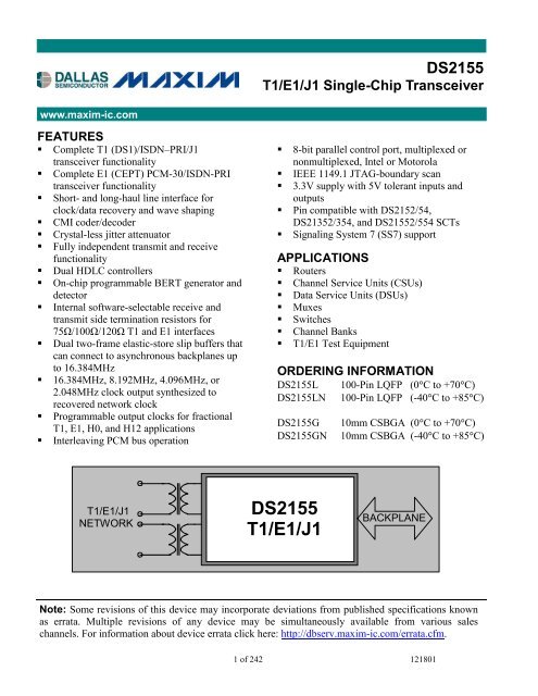
<strong>DS2155</strong><strong>T1</strong>/<strong>E1</strong>/<strong>J1</strong> Single-Chip Transceiverwww.maxim-ic.comFEATURESComplete <strong>T1</strong> (DS1)/ISDN–PRI/<strong>J1</strong>transceiver functionalityComplete <strong>E1</strong> (CEPT) PCM-30/ISDN-PRItransceiver functionalityShort- and long-haul line interface forclock/data recovery and wave shapingCMI coder/decoderCrystal-less jitter attenuatorFully independent transmit and receivefunctionalityDual HDLC controllersOn-chip programmable BERT generator anddetectorInternal software-selectable receive andtransmit side termination resistors for75/100/120 <strong>T1</strong> and <strong>E1</strong> interfacesDual two-frame elastic-store slip buffers thatcan connect to asynchronous backplanes upto 16.384MHz16.384MHz, 8.192MHz, 4.096MHz, or2.048MHz clock output synthesized torecovered network clockProgrammable output clocks for fractional<strong>T1</strong>, <strong>E1</strong>, H0, and H12 applicationsInterleaving PCM bus operation 8-bit parallel control port, multiplexed ornonmultiplexed, Intel or Motorola IEEE 1149.1 JTAG-boundary scan 3.3V supply with 5V tolerant inputs andoutputs Pin compatible with DS2152/54,DS21352/354, and <strong>DS2155</strong>2/554 SCTs Signaling System 7 (SS7) supportAPPLICATIONSRoutersChannel Service Units (CSUs)Data Service Units (DSUs)MuxesSwitchesChannel Banks<strong>T1</strong>/<strong>E1</strong> Test EquipmentORDERING INFORMATION<strong>DS2155</strong>L<strong>DS2155</strong>LN100-Pin LQFP (0C to +70C)100-Pin LQFP (-40C to +85C)<strong>DS2155</strong>G 10mm CSBGA (0C to +70C)<strong>DS2155</strong>GN 10mm CSBGA (-40C to +85C)<strong>T1</strong>/<strong>E1</strong>/<strong>J1</strong>NETWORK<strong>DS2155</strong><strong>T1</strong>/<strong>E1</strong>/<strong>J1</strong>BACKPLANENote: Some revisions of this device may incorporate deviations from published specifications knownas errata. Multiple revisions of any device may be simultaneously available from various saleschannels. For information about device errata click here: http://dbserv.maxim-ic.com/errata.cfm.1 of 242 121801
2 of 242<strong>DS2155</strong>1. DESCRIPTIONThe <strong>DS2155</strong> can be software configured for <strong>T1</strong>, <strong>E1</strong>, or <strong>J1</strong> operation. It is composed of a line interfaceunit (LIU), framer, HDLC controllers, and a TDM backplane interface, and is controlled via an 8-bitparallel port configured for Intel or Motorola bus operations.The LIU is composed of a transmit interface, receive interface, and a jitter attenuator. The transmitinterface is responsible for generating the necessary wave shapes for driving the network and providingthe correct source impedance depending on the type of media used. <strong>T1</strong> waveform generation includesDSX–1 line build-outs as well as CSU line build-outs of -7.5dB, -15dB, and -22.5dB. <strong>E1</strong> waveformgeneration includes G.703 wave shapes for both 75 coax and 120 twisted cables. The receive interfaceprovides network termination and recovers clock and data from the network. The receive sensitivityadjusts automatically to the incoming signal and can be programmed for 0dB to 43dB or 0dB to 12dB for<strong>E1</strong> applications and 0dB to 30dB or 0dB to 36dB for <strong>T1</strong> applications. The jitter attenuator removes phasejitter from the transmitted or received signal. The crystal-less jitter attenuator requires only a 2.048MHzMCLK for both <strong>E1</strong> and <strong>T1</strong> applications (with the option of using a 1.544MHz MCLK in <strong>T1</strong> applications)and can be placed in either transmit or receive data paths. An additional feature of the LIU is a CMIcoder/decoder for interfacing to optical networks.On the transmit side, clock data and frame-sync signals are provided to the framer by the backplaneinterface section. The framer inserts the appropriate synchronization framing patterns, alarm information,calculates and inserts the CRC codes, and provides the B8ZS/HDB3 (zero code suppression) and AMIline coding. The receive-side framer decodes AMI, B8ZS, and HDB3 line coding, synchronizes to thedata stream, reports alarm information, counts framing/coding/CRC errors, and provides clock/data andframe-sync signals to the backplane interface section.Both the transmit and receive path have two HDLC controllers. The HDLC controllers transmit andreceive data via the framer block. The HDLC controllers can be assigned to any time slot, group of timeslots, portion of a time slot or to FDL (<strong>T1</strong>) or Sa bits (<strong>E1</strong>). Each controller has 128-bit FIFOs, thusreducing the amount of processor overhead required to manage the flow of data. In addition, built-insupport for reducing the processor time required handles SS7 applications.The backplane interface provides a versatile method of sending and receiving data from the host system.Elastic stores provide a method for interfacing to asynchronous systems, converting from a <strong>T1</strong>/<strong>E1</strong>network to a 2.048MHz, 4.096MHz, 8.192MHz or N x 64kHz system backplane. The elastic stores alsomanage slip conditions (asynchronous interface). An interleave bus option (IBO) is provided to allowmultiple <strong>DS2155</strong>s to share a high-speed backplane.The parallel port provides access for control and configuration of all the <strong>DS2155</strong>’s features. Up to eight<strong>DS2155</strong>’s interrupt or user-selectable alarm status information can be accessed using a single host CPUread of any one of the eight devices via the extended system information bus (ESIB) function. Diagnosticcapabilities include loopbacks, PRBS pattern generation/detection, and 16-bit loop-up and loop-downcode generation and detection.The device fully meets all of the latest <strong>E1</strong> and <strong>T1</strong> specifications, including the following: ANSI: <strong>T1</strong>.403-1995, <strong>T1</strong>.231-1993, <strong>T1</strong>.408 AT&T: TR54016, TR62411 ITU: G.703, G.704, G.706, G.736, G.775, G.823, G.932, I.431, O.151, O.161 ETSI: ETS 300 011, ETS 300 166, ETS 300 233, CTR4, CTR12 Japanese: JTG.703, JTI.431, JJ-20.11 (CMI coding only)
3 of 242<strong>DS2155</strong>1.1 FEATURE HIGHLIGHTSThe <strong>DS2155</strong> contains all of the features of the previous generation of Dallas Semiconductor’s <strong>T1</strong> and <strong>E1</strong>SCTs plus many new features.1.1.1 General100-pin LQFP package (14mm x 14mm)3.3V supply with 5V tolerant inputs and outputsPin compatible with DS2152/54, DS352/354, and DS552/554 SCTsEvaluation kitsIEEE 1149.1 JTAG-boundary scanDriver source code available from the factory1.1.2 Line InterfaceRequires a single master clock (MCLK) for both <strong>E1</strong> and <strong>T1</strong> operation. Master clock can be2.048MHz, 4.096MHz, 8.192MHz, or 16.384MHz. Option to use 1.544MHz, 3.088MHz,6.276MHz, or 12.552MHz for <strong>T1</strong>-only operationFully software configurableShort- and long-haul applicationsAutomatic receive sensitivity adjustmentsRanges include 0dB to -43dB or 0dB to -15dB for <strong>E1</strong> applications; 0dB to -36dB or 0dB to -15dBfor <strong>T1</strong> applicationsReceive level indication in 2.5dB steps from -42.5dB to -2.5dBInternal receive termination option for 75, 100, and 120 linesMonitor application gain settings of 20dB, 26dB, and 32dBG.703 receive-synchronization signal-modeFlexible transmit-waveform generation<strong>T1</strong> DSX-1 line build-outs<strong>T1</strong> CSU line build-outs of -7.5dB, -15dB, and -22.5dB<strong>E1</strong> waveforms include G.703 waveshapes for both 75 coax and 120 twisted cablesAIS generation independent of loopbacksAlternating ones and zeros generationSquare-wave outputOpen-drain output optionNRZ format optionTransmitter power-downTransmitter 50mA short-circuit limiter with exceeded indication of current limitTransmit open-circuit-detected indicationLine interface function can be completely decoupled from the framer/formatter1.1.3 Clock SynthesizerOutput frequencies include 2.048MHz, 4.096MHz, 8.192MHz, and 16.384MHzDerived from recovered receive clock1.1.4 Jitter Attenuator32-bit or 128-bit crystal-less jitter attenuatorRequires only a 2.048MHz master clock for both <strong>E1</strong> and <strong>T1</strong> operation with the option to use1.544MHz for <strong>T1</strong> operationCan be placed in either the receive or transmit path or disabledLimit trip indication
1.1.5 Framer/Formatter Fully independent transmit and receive functionality Full receive- and transmit-path transparency <strong>T1</strong> framing formats include D4 (SLC-96) and ESF Detailed alarm- and status-reporting with optional interrupt support Large path- and line-error counters for: <strong>T1</strong> – BPV, CV, CRC6, and framing bit errors <strong>E1</strong> – BPV, CV, CRC4, E-bit, and frame alignment errors Timed or manual update modes DS1 Idle Code Generation on a per-channel basis in both transmit and receive paths User-defined Digital milliwatt ANSI <strong>T1</strong>.403-1998 support <strong>E1</strong>ETS 300 011 RAI generation G.965 V5.2 link detect Ability to monitor one DS0 channel in both the transmit and receive paths In-band repeating-pattern generators and detectors Three independent generators and detectors Patterns from 1 bit to 8 bits or 16 bits in length RCL, RLOS, RRA, and RAIS alarms now interrupt on change of state Flexible signaling support Software- or hardware-based Interrupt generated on change of signaling data Receive-signaling freeze on loss of sync, carrier loss, or frame slip Addition of hardware pins to indicate carrier loss and signaling freeze Automatic RAI generation to ETS 300 011 specifications Expanded access to Sa and Si bits Option to extend carrier-loss criteria to a 1ms period as per ETS 300 233 Japanese <strong>J1</strong> support Ability to calculate and check CRC6 according to the Japanese standard Ability to generate yellow alarm according to the Japanese standard<strong>DS2155</strong>1.1.6 System Interface Dual two-frame, independent receive and transmit elastic stores Independent control and clocking Controlled-slip capability with status Minimum-delay mode supported Maximum 16.384MHz backplane burst rate Supports <strong>T1</strong> to CEPT (<strong>E1</strong>) conversion Programmable output clocks for fractional <strong>T1</strong>, <strong>E1</strong>, H0, and H12 applications Interleaving PCM bus operation Hardware-signaling capability Receive-signaling reinsertion to a backplane, multiframe sync Availability of signaling in a separate PCM data stream Signaling freezing Ability to pass the <strong>T1</strong> F-bit position through the elastic stores in the 2.048MHz backplane mode Access to the data streams in between the framer/formatter and the elastic stores User-selectable synthesized clock output4 of 242
1.1.7 HDLC ControllersTwo independent HDLC controllersFast load and unload features for FIFOsSS7 support for FISU transmit and receiveIndependent 128-byte RX and TX buffers with interrupt supportAccess FDL, Sa, or single/multiple DS0 channelsDS0 access includes Nx64 or Nx56Compatible with polled or interrupt-driven environmentsBit Oriented Code (BOC) support<strong>DS2155</strong>1.1.8 Test and DiagnosticsProgrammable on-chip Bit Error Rate Testing (BERT)Pseudorandom patterns including QR SSUser-defined repetitive patternsDaly patternError insertion single and continuousTotal-bit and errored-bit countsPayload Error InsertionError insertion in the payload portion of the <strong>T1</strong> frame in the transmit pathErrors can be inserted over the entire frame or selected channelsInsertion options include continuous and absolute number with selectable insertion ratesF-bit corruption for line testingLoopbacks (remote, local, analog, and per-channel loopback)1.1.9 Extended System Information Bus Host can read interrupt and alarm status on up to eight ports with a single-bus read1.1.10 User-Programmable Output Pins Four user-defined output pins for controlling external logic1.1.11 Control Port8-bit parallel control portMultiplexed or nonmultiplexed busesIntel or Motorola formatsSupports polled or interrupt-driven environmentsSoftware access to device ID and silicon revisionSoftware-reset supportedAutomatic clear on power-upFlexible register-space resetsHardware reset pinNote: This data sheet assumes a particular nomenclature of the <strong>T1</strong> and <strong>E1</strong> operating environment. Ineach 125s <strong>T1</strong> frame, there are 24 8-bit channels plus a framing bit. It is assumed that the framing bit issent first followed by channel 1. Each channel is made up of 8 bits, which are numbered 1 to 8. Bit 1, theMSB, is transmitted first. Bit 8, the LSB, is transmitted last. The term “locked” is used to refer to twoclock signals that are phase- or frequency-locked or derived from a common clock (i.e., a 1.544MHzclock can be locked to a 2.048MHz clock if they share the same 8kHz component). Throughout this datasheet, the following abbreviations will be used:5 of 242
TABLE OF CONTENTS1. DESCRIPTION .....................................................................................................................................21.1 FEATURE HIGHLIGHTS .....................................................................................................................31.1.1 General....................................................................................................................................31.1.2 Line Interface ..........................................................................................................................31.1.3 Clock Synthesizer.....................................................................................................................31.1.4 Jitter Attenuator.......................................................................................................................41.1.5 Framer/Formatter ...................................................................................................................41.1.6 System Interface.......................................................................................................................41.1.7 HDLC Controllers ...................................................................................................................51.1.8 Test and Diagnostics ...............................................................................................................51.1.9 Extended System Information Bus ...........................................................................................51.1.10 User-Programmable Output Pins............................................................................................51.1.11 Control Port ............................................................................................................................52. LIST OF FIGURES.............................................................................................................................10<strong>DS2155</strong>3. LIST OF TABLES...............................................................................................................................123.1 DOCUMENT REVISION HISTORY.....................................................................................................134. BLOCK DIAGRAM............................................................................................................................145. PIN FUNCTION DESCRIPTION .....................................................................................................185.1 TRANSMIT SIDE PINS .....................................................................................................................185.2 RECEIVE SIDE PINS ........................................................................................................................205.3 PARALLEL CONTROL PORT PINS ....................................................................................................225.4 EXTENDED SYSTEM INFORMATION BUS.........................................................................................235.5 USER OUTPUT PORT PINS...............................................................................................................235.6 JTAG TEST ACCESS PORT PINS .....................................................................................................245.7 LINE INTERFACE PINS ....................................................................................................................245.8 SUPPLY PINS ..................................................................................................................................255.9 L AND G PACKAGE PINOUT ...........................................................................................................265.10 10MM STBGA PACKAGE...............................................................................................................286. PARALLEL PORT .............................................................................................................................296.1 REGISTER MAP...............................................................................................................................297. SPECIAL PER-CHANNEL REGISTER OPERATION.................................................................348. PROGRAMMING MODEL...............................................................................................................368.1 POWER-UP SEQUENCE ...................................................................................................................378.1.1 Master Mode Register ...........................................................................................................378.2 INTERRUPT HANDLING...................................................................................................................388.3 STATUS REGISTERS........................................................................................................................388.4 INFORMATION REGISTERS..............................................................................................................398.5 INTERRUPT INFORMATION REGISTERS ...........................................................................................399. CLOCK MAP ......................................................................................................................................4010. <strong>T1</strong> FRAMER/FORMATTER CONTROL REGISTERS ............................................................4110.1 <strong>T1</strong> CONTROL REGISTERS ...............................................................................................................4110.2 <strong>T1</strong> TRANSMIT TRANSPARENCY......................................................................................................4610.3 <strong>T1</strong> RECEIVE SIDE DIGITAL MILLIWATT CODE GENERATION..........................................................4610.4 <strong>T1</strong> INFORMATION REGISTER ..........................................................................................................4811. <strong>E1</strong> FRAMER/FORMATTER CONTROL REGISTERS ............................................................5011.1 <strong>E1</strong> CONTROL REGISTERS ...............................................................................................................5011.2 AUTOMATIC ALARM GENERATION ................................................................................................546 of 242
11.3 <strong>E1</strong> INFORMATION REGISTERS ........................................................................................................55<strong>DS2155</strong>12. COMMON CONTROL AND STATUS REGISTERS.................................................................5713. I/O PIN CONFIGURATION OPTIONS.......................................................................................6414. LOOPBACK CONFIGURATION ................................................................................................6414.1 PER-CHANNEL LOOPBACK.............................................................................................................6815. ERROR COUNT REGISTERS .....................................................................................................7015.1 LINE CODE VIOLATION COUNT REGISTER (LCVCR).....................................................................7115.2 PATH CODE VIOLATION COUNT REGISTER (PCVCR)....................................................................7315.3 FRAMES OUT OF SYNC COUNT REGISTER (FOSCR)......................................................................7415.4 E-BIT COUNTER REGISTER (EBCR)...............................................................................................7516. DS0 MONITORING FUNCTION .................................................................................................7616.1 TRANSMIT DS0 MONITOR REGISTERS ...........................................................................................7616.2 RECEIVE DS0 MONITOR REGISTERS ..............................................................................................7717. SIGNALING OPERATION ...........................................................................................................7817.1 RECEIVE SIGNALING ......................................................................................................................7817.1.1 Processor-Based Receive Signaling ......................................................................................7917.1.2 Hardware-Based Receive Signaling......................................................................................7917.2 TRANSMIT SIGNALING ...................................................................................................................8417.2.1 Processor-Based Transmit Signaling ....................................................................................8417.2.2 Software Signaling Insertion Enable Registers, <strong>E1</strong> CAS Mode.............................................9017.2.3 Software Signaling Insertion Enable Registers, <strong>T1</strong> Mode.....................................................9217.2.4 Hardware-Based Transmit Signaling....................................................................................9318. PER-CHANNEL IDLE CODE GENERATION ..........................................................................9418.1 IDLE CODE PROGRAMMING EXAMPLES..........................................................................................9519. CHANNEL BLOCKING REGISTERS ........................................................................................9920. ELASTIC STORES OPERATION..............................................................................................10220.1 RECEIVE SIDE ..............................................................................................................................10520.1.1 <strong>T1</strong> Mode...............................................................................................................................10520.1.2 <strong>E1</strong> Mode ..............................................................................................................................10520.2 TRANSMIT SIDE............................................................................................................................10620.2.1 <strong>T1</strong> Mode...............................................................................................................................10620.2.2 <strong>E1</strong> Mode ..............................................................................................................................10620.3 ELASTIC STORES INITIALIZATION ................................................................................................10620.4 MINIMUM DELAY MODE..............................................................................................................10621. G.706 INTERMEDIATE CRC-4 UPDATING (<strong>E1</strong> MODE ONLY) .........................................10722. <strong>T1</strong> BIT ORIENTED CODE (BOC) CONTROLLER ................................................................10822.1 TRANSMIT BOC...........................................................................................................................10822.2 RECEIVE BOC..............................................................................................................................10823. ADDITIONAL (SA) AND INTERNATIONAL (SI) BIT OPERATION (<strong>E1</strong> ONLY).............11223.1 HARDWARE SCHEME (METHOD 1) ...............................................................................................11223.2 INTERNAL REGISTER SCHEME BASED ON DOUBLE–FRAME (METHOD 2) ....................................11223.3 INTERNAL REGISTER SCHEME BASED ON CRC4 MULTIFRAME...................................................11524. HDLC CONTROLLERS..............................................................................................................12624.1 BASIC OPERATION DETAILS.........................................................................................................12624.2 HDLC CONFIGURATION ..............................................................................................................1287 of 242
24.2.1 FIFO Control ......................................................................................................................13024.3 HDLC MAPPING..........................................................................................................................13124.3.1 Receive.................................................................................................................................13124.3.2 Transmit...............................................................................................................................13324.3.3 FIFO Information................................................................................................................13824.3.4 Receive Packet Bytes Available...........................................................................................13824.3.5 HDLC FIFOs.......................................................................................................................14024.4 RECEIVE HDLC CODE EXAMPLE.................................................................................................14024.5 LEGACY FDL SUPPORT (<strong>T1</strong> MODE).............................................................................................14024.5.1 Receive Section....................................................................................................................14224.5.2 Transmit Section..................................................................................................................14224.6 D4/SLC–96 OPERATION..............................................................................................................14225. LINE INTERFACE UNIT (LIU) .................................................................................................14325.1 LIU OPERATION ..........................................................................................................................14425.2 LIU RECEIVER.............................................................................................................................14425.2.1 Receive Level Indicator .......................................................................................................14425.2.2 Receive G.703 Section 10 Synchronization Signal ..............................................................14525.2.3 Monitor Mode......................................................................................................................14525.3 LIU TRANSMITTER ......................................................................................................................14625.3.1 Transmit Short Circuit Detector / Limiter ...........................................................................14625.3.2 Transmit Open Circuit Detector..........................................................................................14625.3.3 Transmit BPV Error Insertion.............................................................................................14625.3.4 Transmit G.703 Section 10 Synchronization Signal (<strong>E1</strong> Mode) ..........................................14625.4 MCLK PRESCALER......................................................................................................................14625.5 JITTER ATTENUATOR ...................................................................................................................14725.6 CMI (CODE MARK INVERSION) OPTION......................................................................................14725.7 LIU CONTROL REGISTERS ...........................................................................................................14825.8 RECOMMENDED CIRCUITS ...........................................................................................................15725.9 COMPONENT SPECIFICATIONS......................................................................................................15926. PROGRAMMABLE IN-BAND LOOP CODE GENERATION AND DETECTION ............163<strong>DS2155</strong>27. BERT FUNCTION........................................................................................................................17027.1 BERT REGISTER DESCRIPTION....................................................................................................17127.2 BERT REPETITIVE PATTERN SET.................................................................................................17627.3 BERT BIT COUNTER ...................................................................................................................17727.4 BERT ERROR COUNTER ..............................................................................................................17828. PAYLOAD ERROR INSERTION FUNCTION ........................................................................17928.1 NUMBER OF ERRORS REGISTERS .................................................................................................18128.1.1 Number Of Errors Left Register ..........................................................................................18229. INTERLEAVED PCM BUS OPERATION................................................................................18329.1 CHANNEL INTERLEAVE MODE ....................................................................................................18329.2 FRAME INTERLEAVE MODE.........................................................................................................18530. EXTENDED SYSTEM INFORMATION BUS (ESIB) .............................................................18631. PROGRAMMABLE BACKPLANE CLOCK SYNTHESIZER...............................................19032. FRACTIONAL <strong>T1</strong>/<strong>E1</strong> SUPPORT ...............................................................................................19133. USER-PROGRAMMABLE OUTPUT PINS..............................................................................19234. JTAG-BOUNDARY SCAN ARCHITECTURE AND TEST ACCESS PORT .......................19334.1 INSTRUCTION REGISTER...............................................................................................................19734.2 TEST REGISTERS ..........................................................................................................................19834.3 BOUNDARY SCAN REGISTER........................................................................................................19934.4 BYPASS REGISTER........................................................................................................................1998 of 242
34.5 IDENTIFICATION REGISTER ..........................................................................................................199<strong>DS2155</strong>35. FUNCTIONAL TIMING DIAGRAMS.......................................................................................20135.1 <strong>T1</strong> MODE .....................................................................................................................................20235.2 <strong>E1</strong> MODE .....................................................................................................................................21236. OPERATING PARAMETERS....................................................................................................22537. AC TIMING PARAMETERS AND DIAGRAMS .....................................................................22737.1 MULTIPLEXED BUS AC CHARACTERISTICS .................................................................................22737.2 NONMULTIPLEXED BUS AC CHARACTERISTICS...........................................................................23037.3 RECEIVE SIDE AC CHARACTERISTICS..........................................................................................23337.4 TRANSMIT AC CHARACTERISTICS ...............................................................................................23738. MECHANICAL DESCRIPTION ................................................................................................24138.1 L PACKAGE..................................................................................................................................24138.2 G PACKAGE .................................................................................................................................2429 of 242
2. LIST OF FIGURESFigure 4-1 <strong>DS2155</strong> BLOCK DIAGRAM......................................................................................................14Figure 4-2 LINE INTERFACE UNIT...........................................................................................................15Figure 4-3 RECEIVE AND TRANSMIT FRAMER ....................................................................................16Figure 4-4 BACKPLANE INTERFACE .....................................................................................................17Figure 5-1 10mm STBGA PACKAGE PIN LAYOUT ................................................................................28Figure 8-1 <strong>DS2155</strong> PROGRAMMING SEQUENCE ...................................................................................36Figure 9-1 <strong>DS2155</strong> CLOCK MAP ................................................................................................................40Figure 17-1 SIMPLIFIED DIAGRAM OF RECEIVE SIGNALING PATH ...............................................78Figure 17-2 SIMPLIFIED DIAGRAM OF TRANSMIT SIGNALING PATH............................................84Figure 21-1 CRC-4 RECALCULATE METHOD ......................................................................................107Figure 25-1 BASIC NETWORK CONNECTIONS....................................................................................143Figure 25-2 TYPICAL MONITOR APPLICATION..................................................................................145Figure 25-3 CMI CODING .........................................................................................................................146Figure 25-4 BASIC INTERFACE...............................................................................................................157Figure 25-5 PROTECTED INTERFACE USING INTERNAL RECEIVE TERMINATION ...................158Figure 25-6 <strong>E1</strong> TRANSMIT PULSE TEMPLATE.....................................................................................160Figure 25-7 <strong>T1</strong> TRANSMIT PULSE TEMPLATE.....................................................................................160Figure 25-8 JITTER TOLERANCE (<strong>T1</strong> MODE).......................................................................................161Figure 25-9 JITTER TOLERANCE (<strong>E1</strong> MODE).......................................................................................161Figure 25-10 JITTER ATTENUATION (<strong>T1</strong> MODE) ................................................................................162Figure 25-11 JITTER ATTENUATION (<strong>E1</strong> MODE) ................................................................................162Figure 25-12 OPTIONAL CRYSTAL CONNECTIONS ...........................................................................163Figure 29-1 IBO EXAMPLE.......................................................................................................................185Figure 30-1 ESIB GROUP OF FOUR <strong>DS2155</strong>s.........................................................................................186Figure 34-1 JTAG FUNCTIONAL BLOCK DIAGRAM...........................................................................193Figure 34-2 TAP CONTROLLER STATE DIAGRAM .............................................................................195Figure 35-1 RECEIVE SIDE D4 TIMING .................................................................................................202Figure 35-2 RECEIVE SIDE ESF TIMING ...............................................................................................203Figure 35-3 RECEIVE SIDE BOUNDARY TIMING (With Elastic Store Disabled)................................204Figure 35-4 RECEIVE SIDE 1.544MHz BOUNDARY TIMING (With Elastic Store Enabled)...............205Figure 35-5 RECEIVE SIDE 2.048MHz BOUNDARY TIMING (With Elastic Store Enabled)...............206Figure 35-6 TRANSMIT SIDE D4 TIMING..............................................................................................207Figure 35-7 TRANSMIT SIDE ESF TIMING............................................................................................208Figure 35-8 TRANSMIT SIDE BOUNDARY TIMING (With Elastic Store Disabled) ............................209Figure 35-9 TRANSMIT SIDE 1.544MHz BOUNDARY TIMING (With Elastic Store Enabled) ...........210Figure 35-10 TRANSMIT SIDE 2.048MHz BOUNDARY TIMING (With Elastic Store Enabled) .........211Figure 35-11 RECEIVE SIDE TIMING .....................................................................................................212Figure 35-12 RECEIVE SIDE BOUNDARY TIMING (With Elastic Store Disabled)..............................213Figure 35-13 RECEIVE SIDE BOUNDARY TIMING, RSYSCLK = 1.544MHz (Elastic Store Enabled)214Figure 35-14 RECEIVE SIDE BOUNDARY TIMING, RSYSCLK = 2.048MHz (Elastic Store Enabled)215Figure 35-15 RECEIVE IBO CHANNEL INTERLEAVE MODE TIMING.............................................216Figure 35-16 RECEIVE IBO FRAME INTERLEAVE MODE TIMING ..................................................217Figure 35-17 G.802 TIMING, <strong>E1</strong> MODE ONLY.......................................................................................218Figure 35-18 TRANSMIT SIDE TIMING..................................................................................................219Figure 35-19 TRANSMIT SIDE BOUNDARY TIMING (Elastic Store Diabled).....................................220Figure 35-20 TRANSMIT SIDE BOUNDARY TIMING, TSYSCLK = 1.544MHz .................................221Figure 35-21 TRANSMIT SIDE BOUNDARY TIMING, TSYSCLK = 2.048MHz .................................222Figure 35-22 TRANSMIT IBO CHANNEL INTERLEAVE MODE TIMING .........................................223Figure 35-23 TRANSMIT IBO FRAME INTERLEAVE MODE TIMING...............................................224Figure 37-1 INTEL BUS READ TIMING (BTS = 0 / MUX = 1) ..............................................................228Figure 37-2 INTEL BUS WRITE TIMING (BTS = 0 / MUX = 1) ............................................................228Figure 37-3 MOTOROLA BUS TIMING (BTS = 1 / MUX = 1)...............................................................229Figure 37-4 INTEL BUS READ TIMING (BTS = 0 / MUX = 0) ..............................................................231Figure 37-5 INTEL BUS WRITE TIMING (BTS = 0 / MUX = 0) ............................................................231Figure 37-6 MOTOROLA BUS READ TIMING (BTS = 1 / MUX = 0)...................................................232Figure 37-7 MOTOROLA BUS WRITE TIMING (BTS = 1 / MUX = 0) .................................................232Figure 37-8 RECEIVE SIDE TIMING (<strong>T1</strong> MODE) ..................................................................................234Figure 37-9 RECEIVE SIDE TIMING, ELASTIC STORE ENABLED (<strong>T1</strong> MODE)...............................235Figure 37-10 RECEIVE LINE INTERFACE TIMING ..............................................................................23610 of 242<strong>DS2155</strong>
Figure 37-11 TRANSMIT SIDE TIMING..................................................................................................238Figure 37-12 TRANSMIT SIDE TIMING, ELASTIC STORE ENABLED ..............................................239Figure 37-13 TRANSMIT LINE INTERFACE TIMING...........................................................................240<strong>DS2155</strong>11 of 242
3. LIST OF TABLESTable 5-1 PIN DESCRIPTION SORTED BY PIN NUMBER.....................................................................26Table 6-1 REGISTER MAP SORTED BY ADDRESS................................................................................29Table 10-1 <strong>T1</strong> ALARM CRITERIA .............................................................................................................49Table 11-1 <strong>E1</strong> SYNC/RESYNC CRITERIA ................................................................................................51Table 11-2 <strong>E1</strong> ALARM CRITERIA .............................................................................................................56Table 15-1 <strong>T1</strong> LINE CODE VIOLATION COUNTING OPTIONS............................................................71Table 15-2 <strong>E1</strong> LINE CODE VIOLATION COUNTING OPTIONS............................................................71Table 15-3 <strong>T1</strong> PATH CODE VIOLATION COUNTING ARRANGEMENTS...........................................73Table 15-4 <strong>T1</strong> FRAMES OUT OF SYNC COUNTING ARRANGEMENTS.............................................73Table 17-1 TIME SLOT NUMBERING SCHEMES ...................................................................................85Table 18-1 IDLE CODE ARRAY ADDRESS MAPPING...........................................................................94Table 20-1 ELASTIC STORE DELAY AFTER INITIALIZATION.........................................................106Table 24-1 HDLC CONTROLLER REGISTERS ......................................................................................127Table 25-1 TRANSFORMER SPECIFICATIONS.....................................................................................159Table 28-1 TRANSMIT ERROR INSERTION SETUP SEQUENCE .......................................................179Table 28-2 ERROR INSERTION EXAMPLES .........................................................................................181Table 34-1 INSTRUCTION CODES FOR IEEE 1149.1 ARCHITECTURE ............................................197Table 34-2 ID CODE STRUCTURE ..........................................................................................................198Table 34-3 DEVICE ID CODES.................................................................................................................198Table 34-4 BOUNDARY SCAN CONTROL BITS...................................................................................200<strong>DS2155</strong>12 of 242
<strong>DS2155</strong>3.1 DOCUMENT REVISION HISTORY1) Initial Preliminary Release, 0312012) Correct text on SR2, SR3, SR4 operation, 0426013) Correct status register operation details, 0504014) Remove references to TTL levels, 0507015) Remove reference to FMS pin; correct basic LIU connections diagram, 0518016) Add section on Clock Map, 0531017) Correct <strong>T1</strong> pre-scale values LIC4 register; add jitter tolerance curve for <strong>E1</strong> mode; correct sample codefor receiving an HDLC message; add capacitive test loads information, 0612018) Add <strong>E1</strong> functional timing diagrams; improve block diagrams, 0625019) Add status register description to LIU section, 08140110) Add text on interrupt usage, 09050111) Change t DHW timing spec for muxed bus operation from 0ns to 5ns. Removed t DDR min value, 10220113 of 242
<strong>DS2155</strong>4. BLOCK DIAGRAMA simplified block diagram showing the major components of the <strong>DS2155</strong> is shown in Figure 4-1. Detailsare shown in subsequent figures. The block diagram is then divided into three functional blocks: LIU,framer, and backplane interface.<strong>DS2155</strong> BLOCK DIAGRAM Figure 4-1CLOCKCLOCKADAPTEREXTERNAL ACCESSTO RECEIVE SIGNALS<strong>T1</strong>/<strong>E1</strong>/<strong>J1</strong>NETWORKRXLIUTXLIULOCAL LOOPBACKJITTER ATTENUATORREMOTE LOOPBACKMUXMUXFRAMER LOOPBACKHDB3/B8ZSSYNCSIGNALINGALARM DETHDLCsFRAMERSIGNALINGALARM GENHDLCsCRC GENHDB3/B8ZSPAYLOAD LOOPBACKBACKPLANECLOCK SYNTHBACKPLANEINTERFACECIRCUITBACKPLANELIU EXTERNAL ACCESSFRAMER BACKPLANETO TRANSMIT SIGNALSINTERFACEJTAGHOST INTERFACEESIB14 of 242
LINE INTERFACE UNIT Figure 4-2<strong>DS2155</strong>RPOSIRCLKIRNEGIRNEGORCLKORPOSO8XCLKXTALDMCLKRCLVCO / PLL32.768MHzMUXJACLKRRINGRTIPTRINGTTIPRECEIVELINE I/FTRANSMITLINE I/FLOCAL LOOPBACKJITTER ATTENUATORTRANSMITOR RECEIVE PATHREMOTE LOOPBACKRPOSRNEGRCLKTPOSTNEGTCLKMUXTPOSOTCLKOTNEGOTNEGITCLKITPOSILIUC15 of 242
RECEIVE AND TRANSMIT FRAMER Figure 4-3<strong>DS2155</strong>RECHDLC #1RECHDLC #2128 ByteFIFO128 ByteFIFODATAMAPPERMAPPERDATARPOSRNEGRCLKTPOSTNEGTCLKFramer LoopbackRECEIVE SIDEFRAMERTRANSMIT SIDEFRAMERCLOCKSYNCSYNCCLOCKCLOCKSYNCSYNCCLOCKDATAMAPPERMAPPERDATAXMITHDLC #1XMITHDLC #2128 ByteFIFO128 ByteFIFO16 of 242
BACKPLANE INTERFACE Figure 4-4<strong>DS2155</strong>Sa BIT/FDLEXTRACTIONRLINKRLCLKSIGNALINGBUFFERRSIGRSIGFRDATACLOCKSYNCELASTICSTORERSYSCLKRSERRCLKRSYNCRMSYNCRFSYNCRDATACHANNELTIMINGRCHCLKRCHBLKSYNCDATACLOCKSa/FDLINSERTELASTICSTORESIGNALINGBUFFERTSERTSIGTSSYNCTSYSCLKTSYNCTESOTDATATLCLKTLINKCHANNELTIMINGTCHCLKTCHBLKJACLKTCLKMUXTCLK17 of 242
5. PIN FUNCTION DESCRIPTION<strong>DS2155</strong>5.1 Transmit Side PinsSignal Name:TCLKSignal Description: Transmit ClockSignal Type:InputA 1.544 MHz or a 2.048MHz primary clock. Used to clock data through the transmit-side formatter.Signal Name:TSERSignal Description: Transmit Serial DataSignal Type:InputTransmit NRZ serial data. Sampled on the falling edge of TCLK when the transmit-side elastic store is disabled. Sampled onthe falling edge of TSYSCLK when the transmit-side elastic store is enabled.Signal Name:TCHCLKSignal Description: Transmit Channel ClockSignal Type:OutputA 192kHz (<strong>T1</strong>) or 256kHz (<strong>E1</strong>) clock that pulses high during the LSB of each channel. Can also be programmed to output agated transmit-bit clock for fractional <strong>T1</strong>/<strong>E1</strong> applications. Synchronous with TCLK when the transmit-side elastic store isdisabled. Synchronous with TSYSCLK when the transmit-side elastic store is enabled. Useful for parallel-to-serial conversionof channel data.Signal Name:TCHBLKSignal Description: Transmit Channel BlockSignal Type:OutputA user-programmable output that can be forced high or low during any of the channels. Synchronous with TCLK when thetransmit-side elastic store is disabled. Synchronous with TSYSCLK when the transmit-side elastic store is enabled. Useful forlocating individual channels in drop-and-insert applications, for external per-channel loopback, and for per-channelconditioning.Signal Name:TSYSCLKSignal Description: Transmit System ClockSignal Type:Input1.544MHz, 2.048MHz, 4.096MHz, 8.192MHz, or 16.384MHz clock. Only used when the transmit-side elastic-store functionis enabled. Should be tied low in applications that do not use the transmit-side elastic store. See Interleaved PCM BusOperation for details on 4.096MHz, 8.192MHz, and 16.384MHz operation using the IBO.Signal Name:TLCLKSignal Description: Transmit Link ClockSignal Type:OutputDemand clock for the transmit link data [TLINK] input.<strong>T1</strong> Mode: A 4kHz or 2kHz (ZBTSI) clock.<strong>E1</strong> Mode: A 4kHz to 20kHz clock.Signal Name:TLINKSignal Description: Transmit Link DataSignal Type:InputIf enabled, this pin will be sampled on the falling edge of TCLK for data insertion into either the FDL stream (ESF) or the Fsbitposition (D4) or the Z–bit position (ZBTSI) or any combination of the Sa bit positions (<strong>E1</strong>).Signal Name:TSYNCSignal Description: Transmit SyncSignal Type:Input/OutputA pulse at this pin will establish either frame or multiframe boundaries for the transmit side. Can be programmed to outputeither a frame or multiframe pulse. If this pin is set to output pulses at frame boundaries, it can also be set via IOCR1.3 tooutput double-wide pulses at signaling frames in <strong>T1</strong> mode.18 of 242
<strong>DS2155</strong>Signal Name:TSSYNCSignal Description: Transmit System SyncSignal Type:InputOnly used when the transmit-side elastic store is enabled. A pulse at this pin will establish either frame or multiframeboundaries for the transmit side. Should be tied low in applications that do not use the transmit-side elastic store.Signal Name:TSIGSignal Description: Transmit Signaling InputSignal Type:InputWhen enabled, this input will sample signaling bits for insertion into outgoing PCM data stream. Sampled on the falling edgeof TCLK when the transmit-side elastic store is disabled. Sampled on the falling edge of TSYSCLK when the transmit-sideelastic store is enabled.Signal Name:TESOSignal Description: Transmit Elastic Store Data OutputSignal Type:OutputUpdated on the rising edge of TCLK with data out of the transmit-side elastic store whether the elastic store is enabled or not.This pin is normally tied to TDATA.Signal Name:TDATASignal Description: Transmit DataSignal Type:InputSampled on the falling edge of TCLK with data to be clocked through the transmit-side formatter. This pin is normally tied toTESO.Signal Name:TPOSOSignal Description: Transmit Positive Data OutputSignal Type:OutputUpdated on the rising edge of TCLKO with the bipolar data out of the transmit-side formatter. Can be programmed to sourceNRZ data via the output-data format (IOCR1.0)-control bit. This pin is normally tied to TPOSI.Signal Name:TNEGOSignal Description: Transmit Negative Data OutputSignal Type:OutputUpdated on the rising edge of TCLKO with the bipolar data out of the transmit-side formatter. This pin is normally tied toTNEGI.Signal Name:TCLKOSignal Description: Transmit Clock OutputSignal Type:OutputBuffered clock that is used to clock data through the transmit-side formatter (either TCLK or RCLKI). This pin is normallytied to TCLKI.Signal Name:TPOSISignal Description: Transmit Positive Data InputSignal Type:InputSampled on the falling edge of TCLKI for data to be transmitted out onto the <strong>T1</strong> line. Can be internally connected to TPOSOby tying the LIUC pin high. TPOSI and TNEGI can be tied together in NRZ applications.Signal Name:TNEGISignal Description: Transmit Negative Data InputSignal Type:InputSampled on the falling edge of TCLKI for data to be transmitted out onto the <strong>T1</strong> line. Can be internally connected to TNEGOby tying the LIUC pin high. TPOSI and TNEGI can be tied together in NRZ applications.Signal Name:TCLKISignal Description: Transmit Clock InputSignal Type:InputLine interface transmit clock. Can be internally connected to TCLKO by tying the LIUC pin high.19 of 242
5.2 Receive Side Pins<strong>DS2155</strong>Signal Name:RLINKSignal Description: Receive Link DataSignal Type:Output<strong>T1</strong> Mode: Updated with either FDL data (ESF) or Fs bits (D4) or Z bits (ZBTSI) one RCLK before the start of a frame.<strong>E1</strong> Mode: Updated with the full <strong>E1</strong> data stream on the rising edge of RCLK.Signal Name:RLCLKSignal Description: Receive Link ClockSignal Type:Output<strong>T1</strong> Mode: A 4kHz or 2kHz (ZBTSI) clock for the RLINK output.<strong>E1</strong> Mode: A 4kHz to 20kHz clock.Signal Name:RCLKSignal Description: Receive ClockSignal Type:Output1.544MHz (<strong>T1</strong>) or 2.048MHz (<strong>E1</strong>) clock that is used to clock data through the receive-side framer.Signal Name:RCHCLKSignal Description: Receive Channel ClockSignal Type:OutputA 192kHz (<strong>T1</strong>) or 256kHz (<strong>E1</strong>) clock that pulses high during the LSB of each channel can also be programmed to output agated receive-bit clock for fractional <strong>T1</strong>/<strong>E1</strong> applications. Synchronous with RCLK when the receive-side elastic store isdisabled. Synchronous with RSYSCLK when the receive-side elastic store is enabled. Useful for parallel-to-serial conversionof channel data.Signal Name:RCHBLKSignal Description: Receive Channel BlockSignal Type:OutputA user-programmable output that can be forced high or low during any of the 24 <strong>T1</strong> or 32 <strong>E1</strong> channels. Synchronous withRCLK when the receive-side elastic store is disabled. Synchronous with RSYSCLK when the receive-side elastic store isenabled. Also useful for locating individual channels in drop-and-insert applications, for external per-channel loopback, andfor per-channel conditioning. See Channel Blocking Registers.Signal Name:RSERSignal Description: Receive Serial DataSignal Type:OutputReceived NRZ serial data. Updated on rising edges of RCLK when the receive-side elastic store is disabled. Updated on therising edges of RSYSCLK when the receive-side elastic store is enabled.Signal Name:RSYNCSignal Description: Receive SyncSignal Type:Input/OutputAn extracted pulse, one RCLK wide, is output at this pin which identifies either frame (IOCR1.5 = 0) or multiframe(IOCR1.5 = 1) boundaries. If set to output-frame boundaries then via IOCR1.6, RSYNC can also be set to output double-widepulses on signaling frames in <strong>T1</strong> mode. If the receive-side elastic store is enabled, then this pin can be enabled to be an inputvia IOCR1.4 at which a frame or multiframe boundary pulse is applied.Signal Name:RFSYNCSignal Description: Receive Frame SyncSignal Type:OutputAn extracted 8kHz pulse, one RCLK wide, is output at this pin, which identifies frame boundaries.Signal Name:RMSYNCSignal Description: Receive Multiframe SyncSignal Type:OutputAn extracted pulse, one RCLK wide (elastic store disabled) or one RSYSCLK wide (elastic store enabled), is output at this pin,which identifies multiframe boundaries.20 of 242
<strong>DS2155</strong>Signal Name:RPOSISignal Description: Receive Positive Data InputSignal Type:InputSampled on the falling edge of RCLKI for data to be clocked through the receive-side framer. RPOSI and RNEGI can be tiedtogether for a NRZ interface. Can be internally connected to RPOSO by tying the LIUC pin high.Signal Name:RNEGISignal Description: Receive Negative Data InputSignal Type:InputSampled on the falling edge of RCLKI for data to be clocked through the receive-side framer. RPOSI and RNEGI can be tiedtogether for a NRZ interface. Can be internally connected to RNEGO by tying the LIUC pin high.Signal Name:RCLKISignal Description: Receive Clock InputSignal Type:InputClock used to clock data through the receive-side framer. This pin is normally tied to RCLKO. Can be internally connected toRCLKO by tying the LIUC pin high.5.3 Parallel Control Port PinsSignal Name:INT*Signal Description: InterruptSignal Type:OutputFlags host controller during events, alarms, and conditions defined in the status registers. Active-low open-drain output.Signal Name:TSTRSTSignal Description: 3-State Control and Device ResetSignal Type:InputA dual-function pin. A zero-to-one transition issues a hardware reset to the <strong>DS2155</strong> register set. A reset clears all configurationregisters. Configuration register contents are set to zero. Leaving TSTRST high will 3-state all output and I/O pins (includingthe parallel control port). Set low for normal operation. Useful in-board level testing.Signal Name:MUXSignal Description: Bus OperationSignal Type:InputSet low to select nonmultiplexed bus operation. Set high to select multiplexed bus operation.Signal Name:AD0 to AD7Signal Description: Data Bus [D0 to D7] or Address/Data BusSignal Type:Input/OutputIn nonmultiplexed bus operation (MUX = 0), it serves as the data bus. In multiplexed bus operation (MUX = 1), it serves as an8-bit, multiplexed address/data bus.Signal Name:A0 to A6Signal Description: Address BusSignal Type:InputIn nonmultiplexed bus operation (MUX = 0), it serves as the address bus. In multiplexed bus operation (MUX = 1), these pinsare not used and should be tied low.Signal Name:BTSSignal Description: Bus Type SelectSignal Type:InputStrap high to select Motorola bus timing; strap low to select Intel bus timing. This pin controls the function of the RD*(DS*),ALE(AS), and WR*(R/W*) pins. If BTS = 1, then these pins assume the function listed in parenthesis ().22 of 242
<strong>DS2155</strong>Signal Name:RD*(DS*)Signal Description: Read Input-Data StrobeSignal Type:InputRD* and DS* are active-low signals. DS active HIGH when MUX = 0. See bus timing diagrams.Signal Name:CS*Signal Description: Chip SelectSignal Type:InputMust be low to read or write to the device. CS* is an active-low signal.Signal Name:ALE(AS)/A7Signal Description: Address Latch Enable(Address Strobe) or A7Signal Type:InputIn nonmultiplexed bus operation (MUX = 0), it serves as the upper address bit. In multiplexed bus operation (MUX = 1), itserves to demultiplex the bus on a positive-going edge.Signal Name:WR*(R/W*)Signal Description: Write Input(Read/Write)Signal Type:InputWR* is an active-low signal.5.4 Extended System Information BusSignal Name:ESIBS0Signal Description: Extended System Information Bus Select 0Signal Type:Input/OutputUsed to group two to eight <strong>DS2155</strong>s into a bus-sharing mode for alarm and status reporting. See Extended System InformationBus (ESIB) for more details.Signal Name:ESIBS1Signal Description: Extended System Information Bus Select 1Signal Type:Input/OutputUsed to group two to eight <strong>DS2155</strong>s into a bus-sharing mode for alarm and status reporting. See Extended System InformationBus (ESIB) for more details.Signal Name:ESIBRDSignal Description: Extended System Information Bus ReadSignal Type:Input/OutputUsed to group two to eight <strong>DS2155</strong>s into a bus-sharing mode for alarm and status reporting. See Extended System InformationBus (ESIB) for more details.5.5 User-Output Port PinsSignal Name:UOP0/1/2/3Signal Description: User Output PortSignal Type:OutputThese output port pins can be set low or high via the CCR4.0 to CCR4.3 control bits. The pins are forced low on power-up andafter any device reset.23 of 242
5.6 JTAG Test Access Port Pins<strong>DS2155</strong>Signal Name:JTRSTSignal Description: IEEE 1149.1 Test ResetSignal Type:InputJTRST is used to asynchronously reset the test access port controller. After power-up, JTRST must be toggled from low tohigh. This action will set the device into the JTAG DEVICE ID mode. Normal device operation is restored by pulling JTRSTlow. JTRST is pulled HIGH internally via a 10k resistor operation.Signal Name:JTMSSignal Description: IEEE 1149.1 Test Mode SelectSignal Type:InputThis pin is sampled on the rising edge of JTCLK and is used to place the test-access port into the various defined IEEE 1149.1states. This pin has a 10k pullup resistor.Signal Name:JTCLKSignal Description: IEEE 1149.1 Test Clock SignalSignal Type:InputThis signal is used to shift data into JTDI on the rising edge and out of JTDO on the falling edge.Signal Name:JTDISignal Description: IEEE 1149.1 Test Data InputSignal Type:InputTest instructions and data are clocked into this pin on the rising edge of JTCLK. This pin has a 10k pullup resistor.Signal Name:JTDOSignal Description: IEEE 1149.1 Test Data OutputSignal Type:OutputTest instructions and data are clocked out of this pin on the falling edge of JTCLK. If not used, this pin should be leftunconnected.5.7 Line Interface PinsSignal Name:MCLKSignal Description: Master Clock InputSignal Type:InputA (50ppm) clock source. This clock is used internally for both clock/data recovery and for the jitter attenuator for both <strong>T1</strong> and<strong>E1</strong> modes. A quartz crystal of 2.048MHz can be applied across MCLK and XTALD instead of the clock source. The clock ratecan be 16.384MHz, 8.192MHz, 4.096MHz, or 2.048MHz. When using the <strong>DS2155</strong> in <strong>T1</strong>-only operation a 1.544MHz (50ppm)clock source can be used.Signal Name:XTALDSignal Description: Quartz Crystal DriverSignal Type:OutputA quartz crystal of 2.048MHz (optional 1.544MHz in <strong>T1</strong>-only operation) can be applied across MCLK and XTALD instead ofa clock source at MCLK. Leave open-circuited if a clock source is applied at MCLK.Signal Name:8XCLKSignal Description: Eight Times ClockSignal Type:OutputAn 8x clock that is locked to the recovered network clock provided from the clock/data recovery block (if the jitter attenuatoris enabled on the receive side) or from the TCLKI pin (if the jitter attenuator is enabled on the transmit side).24 of 242
<strong>DS2155</strong>Signal Name:LIUCSignal Description: Line Interface ConnectSignal Type:InputTie low to separate the line interface circuitry from the framer/formatter circuitry and activate theTPOSI/TNEGI/TCLKI/RPOSI/RNEGI/RCLKI pins. Tie high to connect the line interface circuitry to the framer/formattercircuitry and deactivate the TPOSI/TNEGI/TCLKI/RPOSI/RNEGI/RCLKI pins. When LIUC is tied high, thePOSI/TNEGI/TCLKI/ RPOSI/RNEGI/RCLKI pins should be tied low.Signal Name:RTIP and RRINGSignal Description: Receive Tip and RingSignal Type:InputAnalog inputs for clock recovery circuitry. These pins connect via a 1:1 transformer to the network. See Line Interface Unit fordetails.Signal Name:TTIP and TRINGSignal Description: Transmit Tip and RingSignal Type:OutputAnalog line driver outputs. These pins connect via a 1:2 step-up transformer to the network. See Line Interface Unit for details.5.8 Supply PinsSignal Name:DV DDSignal Description: Digital Positive SupplySignal Type:Supply3.3V ±5%. Should be tied to the RV DD and TV DD pins.Signal Name:RV DDSignal Description: Receive Analog Positive SupplySignal Type:Supply3.3V ±5%. Should be tied to the DV DD and TV DD pins.Signal Name:TV DDSignal Description: Transmit Analog Positive SupplySignal Type:Supply3.3V ±5% Should be tied to the RV DD and DV DD pins.Signal Name:DV SSSignal Description: Digital Signal GroundSignal Type:SupplyShould be tied to the RV SS and TV SS pins.Signal Name:RV SSSignal Description: Receive Analog Signal GroundSignal Type:Supply0.0V. Should be tied to DV SS and TV SS .Signal Name:TV SSSignal Description: Transmit Analog Signal GroundSignal Type:Supply0.0V. Should be tied to DV SS and RV SS .25 of 242
5.9 L and G Package PinoutThe <strong>DS2155</strong> is available in either a 100-pin LQFP (L) or 10mm µBGA- 0.8mm pitch (G) package.PIN DESCRIPTION SORTED BY PIN NUMBER Table 5-1PIN L PIN G SYMBOL TYPE DESCRIPTION1 A1 RCHBLK O Receive Channel Block2 B2 JTMS I IEEE 1149.1 Test Mode Select3 C3 BPCLK O Back Plane Clock4 B1 JTCLK I IEEE 1149.1 Test Clock Signal5 D4 JTRST I IEEE 1149.1 Test Reset6 C2 RCL O Receive Carrier Loss7 C1 JTDI I IEEE 1149.1 Test Data Input8 D3 UOP0 O User Output 09 D2 UOP1 O User Output 110 D1 JTDO O IEEE 1149.1 Test Data Output11 E3 BTS I Bus Type Select12 E2 LIUC I Line Interface Connect13 <strong>E1</strong> 8XCLK O Eight Times Clock14 E4 TSTRST I Test/Reset15 E5 UOP2 O User Output 216 F1 RTIP I Receive Analog Tip Input17 F2 RRING I Receive Analog Ring Input18 F3 RV DD – Receive Analog Positive Supply19 G1 RV SS – Receive Analog Signal Ground20 F4 RV SS – Receive Analog Signal Ground21 G2 MCLK I Master Clock Input22 H1 XTALD O Quartz Crystal Driver23 G3 UOP3 O User Output 324 <strong>J1</strong> RV SS – Receive Analog Signal Ground25 H2 INT* O Interrupt26 NC – Reserved for Factory Test27 NC – Reserved for Factory Test28 NC – Reserved for Factory Test29 K2 TTIP O Transmit Analog Tip Output30 G4 TV SS – Transmit Analog Signal Ground31 J3 TV DD – Transmit Analog Positive Supply32 K3 TRING O Transmit Analog Ring Output33 H4 TCHBLK O Transmit Channel Block34 J4 TLCLK O Transmit Link Clock35 K4 TLINK I Transmit Link Data36 H5 ESIBS0 I/O Extended System Information Bus 037 J5 TSYNC I/O Transmit Sync38 K5 TPOSI I Transmit Positive Data Input39 G5 TNEGI I Transmit Negative Data Input40 F5 TCLKI I Transmit Clock Input41 K6 TCLKO O Transmit Clock Output42 J6 TNEGO O Transmit Negative Data Output43 H6 TPOSO O Transmit Positive Data Output44 K7 DV DD – Digital Positive Supply45 G6 DV SS – Digital Signal Ground46 J7 TCLK I Transmit Clock47 K8 TSER I Transmit Serial Data48 H7 TSIG I Transmit Signaling Input49 K9 TESO O Transmit Elastic Store Output26 of 242<strong>DS2155</strong>
PIN L PIN G SYMBOL TYPE DESCRIPTION50 J8 TDATA I Transmit Data51 K10 TSYSCLK I Transmit System Clock52 J9 TSSYNC I Transmit System Sync53 H8 TCHCLK O Transmit Channel Clock54 <strong>J1</strong>0 ESIBS1 I/O Extended System Information Bus 155 G7 MUX I Bus Operation56 H9 D0/AD0 I/O Data Bus Bit 0/Address/Data Bus Bit 057 H10 D1/AD1 I/O Data Bus Bit 1/Address/Data Bus Bit 158 G8 D2/AD2 I/O Data Bus Bit 2/Address/Data Bus 259 G9 D3/AD3 I/O Data Bus Bit 3/Address/Data Bus Bit 360 G10 DV SS – Digital Signal Ground61 F8 DVDD - Digital Positive Supply62 F9 D4/AD4 I/O Data Bus Bit 4/Address/Data Bus Bit 463 F10 D5/AD5 I/O Data Bus Bit 5/Address/Data Bus Bit 564 F7 D6/AD6 I/O Data Bus Bit 6/Address/Data Bus Bit 665 F6 D7/AD7 I/O Data Bus Bit 7/Address/Data Bus Bit 766 <strong>E1</strong>0 A0 I Address Bus Bit 067 E9 A1 I Address Bus Bit 168 E8 A2 I Address Bus Bit 269 D10 A3 I Address Bus Bit 370 E7 A4 I Address Bus Bit 471 D9 A5 I Address Bus Bit 572 C10 A6 I Address Bus Bit 673 D8 ALE (AS)/A7 I Address Latch Enable/Address Bus Bit 774 B10 RD*(DS*) I Read Input(Data Strobe)75 C9 CS* I Chip Select76 A10 ESIBRD I/O Extended System Information Bus Read77 B9 WR*(R/W*) I Write Input(Read/Write)78 C8 RLINK O Receive Link Data79 A9 RLCLK O Receive Link Clock80 D7 DV SS – Digital Signal Ground81 B8 DV DD – Digital Positive Supply82 A8 RCLK O Receive Clock83 C7 DV DD – Digital Positive Supply84 B7 DV SS – Digital Signal Ground85 A7 RDATA O Receive Data86 C6 RPOSI I Receive Positive Data Input87 B6 RNEGI I Receive Negative Data Input88 A6 RCLKI I Receive Clock Input89 D6 RCLKO O Receive Clock Output90 E6 RNEGO O Receive Negative Data Output91 A5 RPOSO O Receive Positive Data Output92 B5 RCHCLK O Receive Channel Clock93 C5 RSIGF O Receive Signaling Freeze Output94 A4 RSIG O Receive Signaling Output95 D5 RSER O Receive Serial Data96 B4 RMSYNC O Receive Multiframe Sync97 A3 RFSYNC O Receive Frame Sync98 C4 RSYNC I/O Receive Sync99 A2 RLOS/LOTC O Receive Loss Of Sync/Loss Of Transmit Clock100 B3 RSYSCLK I Receive System Clock<strong>DS2155</strong>27 of 242
5.10 10mm STBGA Package<strong>DS2155</strong>10mm STBGA PACKAGE PIN LAYOUT Figure 5-11 2 3 4 5 6 7 8 9 10ARCHBLK RLOS/LOTCRFSYNC RSIG RPOSO RCLKI RDATA RCLK RLCLK ESIBRDBJTCLK JTMS RSYSCLK RMSYNC RCHCLK RNEGI DVSS DVDD WR*(R/W*)RD*(DS*)CJTDI RCL BPCLK RSYNC RSIGF RPOSI DV DD RLINK CS* A6DJTDO UOP1 UOP0 JTRST RSER RCLKO DVSS ALE(AS)/A7A5A3EFGHJK8XCLK LIUC BTS TSTRST UOP2 RNEGO A4 A2 A1 A0RTIP RRING RV DD RV SS TCLKI D7/AD7 D6/AD6 DV DD D4/AD4 D5/AD5RVSS MCLK UOP3 TVSS TNEGI DVSS MUX D2/AD2 D3/AD3 DVSSXTALD INT* NC TCHBLK ESIBS0 TPOSO TSIG TCHCLK D0/AD0 D1/AD1RV SS NC TV DD TLCLK TSYNC TNEGO TCLK TDATA TSSYNC ESIBS1NC TTIP TRING TLINK TPOSI TCLKO DV DD TSER TESO TSYSCLKTOP VIEW28 of 242
ADDRESS R/W REGISTER NAMEREGISTERABBREVIATIONPAGE00 Master Mode Register MSTRREG 3701 I/O Configuration Register 1 IOCR1 6402 I/O Configuration Register 2 IOCR2 6503 <strong>T1</strong> Receive Control Register 1 <strong>T1</strong>RCR1 4104 <strong>T1</strong> Receive Control Register 2 <strong>T1</strong>RCR2 4205 <strong>T1</strong> Transmit Control Register 1 <strong>T1</strong>TCR1 4306 <strong>T1</strong> Transmit Control Register 2 <strong>T1</strong>TCR2 4407 <strong>T1</strong> Common Control Register 1 <strong>T1</strong>CCR1 4508 Software Signaling Insertion Enable 1 SSI<strong>E1</strong> 9009 Software Signaling Insertion Enable 2 SSIE2 900A Software Signaling Insertion Enable 3 SSIE3 910B Software Signaling Insertion Enable 4 SSIE4 910C <strong>T1</strong> Receive Digital Milliwatt Enable Register 1 <strong>T1</strong>RDMR1 470D <strong>T1</strong> Receive Digital Milliwatt Enable Register 2 <strong>T1</strong>RDMR2 470E <strong>T1</strong> Receive Digital Milliwatt Enable Register 3 <strong>T1</strong>RDMR3 470F Device Identification Register IDR 5810 Information Register 1 INFO1 4811 Information Register 2 INFO2 15412 Information Register 3 INFO3 551314 Interrupt Information Register 1 IIR1 4015 Interrupt Information Register 2 IIR2 4016 Status Register 1 SR1 15517 Interrupt Mask Register 1 IMR1 15618 Status Register 2 SR2 5819 Interrupt Mask Register 2 IMR2 591A Status Register 3 SR3 601B Interrupt Mask Register 3 IMR3 611C Status Register 4 SR4 621D Interrupt Mask Register 4 IMR4 631E Status Register 5 SR5 1041F Interrupt Mask Register 5 IMR5 10420 Status Register 6 SR6 13521 Interrupt Mask Register 6 IMR6 13622 Status Register 7 SR7 13523 Interrupt Mask Register 7 IMR7 13624 Status Register 8 SR8 11025 Interrupt Mask Register 8 IMR8 11126 Status Register 9 SR9 17427 Interrupt Mask Register 9 IMR9 17528 Per-Channel Pointer Register PCPR 3429 Per-Channel Data Register 1 PCDR1 352A Per-Channel Data Register 2 PCDR2 3529 of 242<strong>DS2155</strong>6. PARALLEL PORTThe SCT is controlled via either a nonmultiplexed (MUX = 0) or a multiplexed (MUX = 1) bus by anexternal microcontroller or microprocessor. The SCT can operate with either Intel or Motorola bus timingconfigurations. If the BTS pin is tied low, Intel timing will be selected; if tied high, Motorola timing willbe selected. All Motorola bus signals are listed in parenthesis (). See the timing diagrams in the ACElectrical Characteristics for more details.6.1 Register MapREGISTER MAP SORTED BY ADDRESS Table 6-1
ADDRESS R/W REGISTER NAMEREGISTERABBREVIATIONPAGE2B Per-Channel Data Register 3 PCDR3 352C Per-Channel Data Register 4 PCDR4 352D Information Register 4 INFO4 1372E Information Register 5 INFO5 1372F Information Register 6 INFO6 13730 Information Register 7 INFO7 5531 HDLC #1 Receive Control H1RC 12932 HDLC #2 Receive Control H2RC 12933 <strong>E1</strong> Receive Control Register 1 <strong>E1</strong>RCR1 5034 <strong>E1</strong> Receive Control Register 2 <strong>E1</strong>RCR2 5135 <strong>E1</strong> Transmit Control Register 1 <strong>E1</strong>TCR1 5236 <strong>E1</strong> Transmit Control Register 2 <strong>E1</strong>TCR2 5337 BOC Control Register BOCC 10138 Receive Signaling Change Of State Information 1 RSINFO1 8339 Receive Signaling Change Of State Information 2 RSINFO2 833A Receive Signaling Change Of State Information 3 RSINFO3 833B Receive Signaling Change Of State Information 4 RSINFO4 833C Receive Signaling Change Of State Interrupt Enable 1 RSCS<strong>E1</strong> 833D Receive Signaling Change Of State Interrupt Enable 2 RSCSE2 833E Receive Signaling Change Of State Interrupt Enable 3 RSCSE3 833F Receive Signaling Change Of State Interrupt Enable 4 RSCSE4 8340 Signaling Control Register SIGCR 8041 Error Count Configuration Register ERCNT 7042 Line Code Violation Count Register 1 LCVCR1 7243 Line Code Violation Count Register 2 LCVCR2 7244 Path Code Violation Count Register 1 PCVCR1 7445 Path Code Violation Count Register 2 PCVCR2 7446 Frames Out of Sync Count Register 1 FOSCR1 7547 Frames Out of Sync Count Register 2 FOSCR2 7548 E-Bit Count Register 1 EBCR1 7549 E-Bit Count Register 2 EBCR2 754A Loopback Control Register LBCR 664B Per-Channel Loopback Enable Register 1 PCLR1 684C Per-Channel Loopback Enable Register 2 PCLR2 684D Per-Channel Loopback Enable Register 3 PCLR3 694E Per-Channel Loopback Enable Register 4 PCLR4 694F Elastic Store Control Register ESCR 10350 Transmit Signaling Register 1 TS1 8651 Transmit Signaling Register 2 TS2 8652 Transmit Signaling Register 3 TS3 8653 Transmit Signaling Register 4 TS4 8654 Transmit Signaling Register 5 TS5 8655 Transmit Signaling Register 6 TS6 8656 Transmit Signaling Register 7 TS7 8657 Transmit Signaling Register 8 TS8 8658 Transmit Signaling Register 9 TS9 8659 Transmit Signaling Register 10 TS10 865A Transmit Signaling Register 11 TS11 865B Transmit Signaling Register 12 TS12 865C Transmit Signaling Register 13 TS13 865D Transmit Signaling Register 14 TS14 865E Transmit Signaling Register 15 TS15 865F Transmit Signaling Register 16 TS16 8660 Receive Signaling Register 1 RS1 81<strong>DS2155</strong>30 of 242
ADDRESS R/W REGISTER NAMEREGISTERABBREVIATIONPAGE61 Receive Signaling Register 2 RS2 8162 Receive Signaling Register 3 RS3 8163 Receive Signaling Register 4 RS4 8164 Receive Signaling Register 5 RS5 8165 Receive Signaling Register 6 RS6 8166 Receive Signaling Register 7 RS7 8167 Receive Signaling Register 8 RS8 8168 Receive Signaling Register 9 RS9 8169 Receive Signaling Register 10 RS10 816A Receive Signaling Register 11 RS11 816B Receive Signaling Register 12 RS12 816C Receive Signaling Register 13 RS13 816D Receive Signaling Register 14 RS14 826E Receive Signaling Register 15 RS15 826F Receive Signaling Register 16 RS16 8270 Common Control Register 1 CCR1 5771 Common Control Register 2 CCR2 19072 Common Control Register 3 CCR3 19173 Common Control Register 4 CCR4 19274 Transmit Channel Monitor Select TDS0SEL 7675 Transmit DS0 Monitor Register TDS0M 7676 Receive Channel Monitor Select RDS0SEL 7777 Receive DS0 Monitor Register RDS0M 7778 Line Interface Control 1 LIC1 14879 Line Interface Control 2 LIC2 1517A Line Interface Control 3 LIC3 1527B Line Interface Control 4 LIC4 1537C7D Transmit Line Build-Out Control TLBC 1507E Idle Array Address Register IAAR 967F Per-Channel Idle Code Value Register PCICR 9680 Transmit Idle Code Enable Register 1 TCIC<strong>E1</strong> 9681 Transmit Idle Code Enable Register 2 TCICE2 9682 Transmit Idle Code Enable Register 3 TCICE3 9783 Transmit Idle Code Enable Register 4 TCICE4 9784 Receive Idle Code Enable Register 1 RCIC<strong>E1</strong> 9785 Receive Idle Code Enable Register 2 RCICE2 9786 Receive Idle Code Enable Register 3 RCICE3 9887 Receive Idle Code Enable Register 4 RCICE4 9888 Receive Channel Blocking Register 1 RCBR1 9989 Receive Channel Blocking Register 2 RCBR2 998A Receive Channel Blocking Register 3 RCBR3 1008B Receive Channel Blocking Register 4 RCBR4 1008C Transmit Channel Blocking Register 1 TCBR1 1008D Transmit Channel Blocking Register 2 TCBR2 1008E Transmit Channel Blocking Register 3 TCBR3 1018F Transmit Channel Blocking Register 4 TCBR4 10190 HDLC #1 Transmit Control H1TC 12891 HDLC #1 FIFO Control H1FC 13092 HDLC #1 Receive Channel Select 1 H1RCS1 13193 HDLC #1 Receive Channel Select 2 H1RCS2 13194 HDLC #1 Receive Channel Select 3 H1RCS3 13195 HDLC #1 Receive Channel Select 4 H1RCS4 13196 HDLC #1 Receive Time Slot Bits/Sa Bits Select H1RTSBS 132<strong>DS2155</strong>31 of 242
ADDRESS R/W REGISTER NAMEREGISTERABBREVIATIONPAGE97 HDLC #1 Transmit Channel Select1 H1TCS1 13398 HDLC #1 Transmit Channel Select 2 H1TCS2 13399 HDLC #1 Transmit Channel Select 3 H1TCS3 1339A HDLC #1 Transmit Channel Select 4 H1TCS4 1339B HDLC #1 Transmit Time Slot Bits/Sa Bits Select H1TTSBS 1349C HDLC #1 Receive Packet Bytes Available H1RPBA 1389D HDLC #1 Transmit FIFO H1TF 1399E HDLC #1 Receive FIFO H1RF 1399F HDLC #1 Transmit FIFO Buffer Available H1TFBA 138A0 HDLC #2 Transmit Control H2TC 128A1 HDLC #2 FIFO Control H2FC 130A2 HDLC #2 Receive Channel Select 1 H2RCS1 131A3 HDLC #2 Receive Channel Select 2 H2RCS2 131A4 HDLC #2 Receive Channel Select 3 H2RCS3 131A5 HDLC #2 Receive Channel Select 4 H2RCS4 131A6 HDLC #2 Receive Time Slot Bits/Sa Bits Select H2RTSBS 132A7 HDLC #2 Transmit Channel Select 1 H2TCS1 133A8 HDLC #2 Transmit Channel Select 2 H2TCS2 133A9 HDLC #2 Transmit Channel Select 3 H2TCS3 133AA HDLC #2 Transmit Channel Select 4 H2TCS4 133AB HDLC #2 Transmit Time Slot Bits/Sa Bits Select H2TTSBS 134AC HDLC #2 Receive Packet Bytes Available H2RPBA 138AD HDLC #2 Transmit FIFO H2TF 139AE HDLC #2 Receive FIFO H2RF 139AF HDLC #2 Transmit FIFO Buffer Available H2TFBA 138B0 Extend System Information Bus Control Register 1 ESIBCR1 187B1 Extend System Information Bus Control Register 2 ESIBCR2 188B2 Extend System Information Bus Register 1 ESIB1 189B3 Extend System Information Bus Register 2 ESIB2 189B4 Extend System Information Bus Register 3 ESIB3 189B5 Extend System Information Bus Register 4 ESIB4 189B6 In-Band Code Control Register IBCC 164B7 Transmit Code Definition Register 1 TCD1 165B8 Transmit Code Definition Register 2 TCD2 165B9 Receive Up Code Definition Register 1 RUPCD1 166BA Receive Up Code Definition Register 2 RUPCD2 166BB Receive Down Code Definition Register 1 RDNCD1 167BC Receive Down Code Definition Register 2 RDNCD2 168BD In-Band Receive Spare Control Register RSCC 168BE Receive Spare Code Definition Register 1 RSCD1 169BF Receive Spare Code Definition Register 2 RSCD2 169C0 Receive FDL Register RFDL 141C1 Transmit FDL Register TFDL 142C2 Receive FDL Match Register 1 RFDLM1 141C3 Receive FDL Match Register 2 RFDLM2 141C4C5 Interleave Bus Operation Control Register IBOC 184C6 Receive Align Frame Register RAF 113C7 Receive Nonalign Frame Register RNAF 113C8 Receive Si Align Frame RSiAF 115C9 Receive Si Nonalign Frame RSiNAF 116CA Receive Remote Alarm Bits RRA 116CB Receive Sa4 Bits RSa4 117CC Receive Sa5 Bits RSa5 117<strong>DS2155</strong>32 of 242
<strong>DS2155</strong>7. SPECIAL PER-CHANNEL REGISTER OPERATIONSome of the features described in the data sheet that operate on a per-channel basis use a special methodfor channel selection. The registers involved are the per-channel pointer registers (PCPR) and per-channeldata registers 1 to 4 (PCDR1–4). The user selects the function(s) that are to be applied on a per-channelbasis by setting the appropriate bit(s) in the PCPR register. The user then writes to the PCDR registers toselect the channels for that function. The following is an example of mapping the transmit and receiveBERT function to channels 9, 10, 11, 12, 20, and 21:Write 11h to PCPRWrite 00h to PCDR1Write 0fh to PCDR2Write 18h to PCDR3Write 00h to PCDR4More information about how to use these per-channel features can be found in their respective sections inthe data sheet.Register Name:Register Description:Register Address:PCPRPer-Channel Pointer Register28hBit # 7 6 5 4 3 2 1 0Name RSAOICS RSRCS RFCS BRCS THSCS PEICS TFCS BTCSDefault 0 0 0 0 0 0 0 0Bit 0/BERT Transmit Channel Select (BTCS).Bit 1/Transmit Fractional Channel Select (TFCS).Bit 2/Payload Error Insert Channel Select (PEICS).Bit 3/Transmit Hardware Signaling Channel Select (THSCS).Bit 4/BERT Receive Channel Select (BRCS).Bit 5/Receive Fractional Channel Select (RFCS).Bit 6/Receive Signaling Reinsertion Channel Select (RSRCS).Bit 7/Receive Signaling All Ones Insertion Channel Select (RSAOICS).34 of 242
<strong>DS2155</strong>Register Name:PCDR1Register Description: Per-Channel Data Register 1Register Address: 29hBit # 7 6 5 4 3 2 1 0NameDefault CH8 CH7 CH6 CH5 CH4 CH3 CH2 CH1Register Name:PCDR2Register Description: Per-Channel Data Register 2Register Address: 2AhBit # 7 6 5 4 3 2 1 0NameDefault CH16 CH15 CH14 CH13 CH12 CH11 CH10 CH9Register Name:PCDR3Register Description: Per-Channel Data Register 3Register Address: 2BhBit # 7 6 5 4 3 2 1 0NameDefault CH24 CH23 CH22 CH21 CH20 CH19 CH18 CH17Register Name:PCDR4Register Description: Per-Channel Data Register 4Register Address: 2ChBit # 7 6 5 4 3 2 1 0NameDefault CH32 CH31 CH30 CH29 CH28 CH27 CH26 CH2535 of 242
<strong>DS2155</strong>8.1 Power-Up SequenceThe <strong>DS2155</strong> contains an on-chip power-up reset function, which automatically clears the writeableregister space immediately after power is supplied to the <strong>DS2155</strong>. The user can issue a chip reset at anytime. Issuing a reset will disrupt traffic flowing through the <strong>DS2155</strong> until the device is reprogrammed.The reset can be issued through hardware using the TSTRST pin or through software using the SFTRSTfunction in the master mode register. The LIRST (LIC2.6) should be toggled from zero to one to reset theline interface circuitry. (It will take the <strong>DS2155</strong> about 40ms to recover from the LIRST bit beingtoggled.) Finally, after the TSYSCLK and RSYSCLK inputs are stable, the receive and transmit elasticstores should be reset (this step can be skipped if the elastic stores are disabled).8.1.1 Master Mode RegisterRegister Name:Register Description:Register Address:MSTRREGMaster Mode Register00hBit # 7 6 5 4 3 2 1 0Name - - - - TES<strong>T1</strong> TEST0 <strong>T1</strong>/<strong>E1</strong> SFTRSTDefault 0 0 0 0 0 0 0 0Bit 0/Software Issued Reset (SFTRST).A 0 to 1 transition causes the register space in the <strong>DS2155</strong> to be cleared. A reset clears all configuration and status registers.The bit automatically clears itself when the reset has completed.Bit 1/<strong>DS2155</strong> Operating Mode (<strong>T1</strong>/<strong>E1</strong>).Used to select the operating mode of the framer/formatter (digital) portion of the 2155. The operating mode of the LIU mustalso be programmed.0 = <strong>T1</strong> operation1 = <strong>E1</strong> operationBits 2, 3/Test Mode Bits (TEST0, TES<strong>T1</strong>).Test modes are used to force the output pins of the 2155 into known states. This can facilitate the checkout of assembliesduring the manufacturing process and also be used to isolate devices from shared buses.TES<strong>T1</strong> TEST0 EFFECT ON OUTPUT PINS0 0 Operate normally0 1 Force all output pins into tristate (including all I/O pins and parallel port pins)1 0 Force all output pins low (including all I/O pins except parallel port pins)1 1 Force all output pins high (including all I/O pins except parallel port pins)Bits 4–7/Unused, must be set to zero for proper operation.37 of 242
<strong>DS2155</strong>9. CLOCK MAPFigure 9-1 shows the clock map of the <strong>DS2155</strong>. The routing for the transmit and receive clocks are shownfor the various loopback modes and jitter attenuator positions. Although there is only one jitter attenuator,which can be placed in the receive or transmit path, two are shown for simplification and clarity.<strong>DS2155</strong> CLOCK MAP Figure 9-1MCLKPRE-SCALER LIC4.MPS0LIC4.MPS12.048 TO 1.544SYNTHESIZERLIC2.3DJA = 18 x PLL8XCLKRXCLKTOLIUTXCLKRCL = 1RCL = 0LOCALLOOPBACKLLB = 0LLB = 1JITTER ATTENUATORSEE LIC1 REGISTERLTCAJAS = 0ORDJA = 1JAS = 1ANDDJA = 0JAS = 0ANDDJA = 0JAS = 1ORDJA = 1LTCAREMOTELOOPBACKRLB = 1RLB = 0DJA = 0FRAMERLOOPBACKFLB = 0FLB = 1RECEIVEFRAMERTRANSMITFORMATTERPAYLOADLOOPBACK(SEE NOTES)PLB = 1PLB = 0ABPCLKSYNTHBTCLKMUXCBPCLKRCLKTCLKThe TCLK MUX is dependent on the state of the TCSS0 and TCSS1 bits in the LIC1 register and thestate of the TCLK pin.TCSS1 TCSS0 TRANSMIT CLOCK SOURCE0 0 The TCLK pin (C) is always the source of Transmit Clock.0 1 Switch to the recovered clock (B) when the signal at the TCLK pin fails totransition after 1 channel time.1 0 Use the scaled signal (A) derived from MCLK as the Transmit Clock. The TCLKpin is ignored.1 1 Use the recovered clock (B) as the Transmit Clock. The TCLK pin is ignored.40 of 242
<strong>DS2155</strong>10. <strong>T1</strong> FRAMER/FORMATTER CONTROL REGISTERSThe <strong>T1</strong> framer portion of the <strong>DS2155</strong> is configured via a set of nine control registers. Typically, thecontrol registers are only accessed when the system is first powered up. Once the <strong>DS2155</strong> has beeninitialized, the control registers will only need to be accessed when there is a change in the systemconfiguration. There are two receive-control registers (<strong>T1</strong>RCR1 and <strong>T1</strong>RCR2), two transmit controlregisters (<strong>T1</strong>TCR1 and <strong>T1</strong>TCR2), and a common control register (<strong>T1</strong>CCR1). Each of these registers isdescribed in this section.10.1 <strong>T1</strong> Control RegistersRegister Name:<strong>T1</strong>RCR1Register Description: <strong>T1</strong> Receive Control Register 1Register Address: 03hBit # 7 6 5 4 3 2 1 0Name - ARC OOF1 OOF2 SYNCC SYNCT SYNCE RESYNCDefault 0 0 0 0 0 0 0 0Bit 0/Resynchronize (RESYNC). When toggled from low to high, a resynchronization of the receive side framer is initiated.Must be cleared and set again for a subsequent resync.Bit 1/Sync Enable (SYNCE).0 = auto resync enabled1 = auto resync disabledBit 2/Sync Time (SYNCT).0 = qualify 10 bits1 = qualify 24 bitsBit 3/Sync Criteria (SYNCC).In D4 Framing Mode.0 = search for Ft pattern, then search for Fs pattern1 = cross couple Ft and Fs patternIn ESF Framing Mode.0 = search for FPS pattern only1 = search for FPS and verify with CRC6Bits 4 to 5/Out Of Frame Select Bits (OOF2, OOF1).OOF2 OOF1 OUT OF FRAME CRITERIA0 0 2/4 frame bits in error0 1 2/5 frame bits in error1 0 2/6 frame bits in error1 1 2/6 frame bits in errorBit 6/Auto Resync Criteria (ARC).0 = resync on OOF or RCL event1 = resync on OOF onlyBit 7/Unused, must be set to zero for proper operation.41 of 242
<strong>DS2155</strong>Register Name:<strong>T1</strong>RCR2Register Description: <strong>T1</strong> Receive Control Register 2Register Address: 04hBit # 7 6 5 4 3 2 1 0Name - RFM RB8ZS RSLC96 RZSE RZBTSI RJC RD4YMDefault 0 0 0 0 0 0 0 0Bit 0/Receive Side D4 Yellow Alarm Select (RD4YM).0 = zeros in bit 2 of all channels1 = a one in the S-bit position of frame 12 (<strong>J1</strong> Yellow Alarm Mode)Bit 1/Receive Japanese CRC6 Enable (RJC).0 = use ANSI/AT&T/ITU CRC6 calculation (normal operation)1 = use Japanese standard JT–G704 CRC6 calculationBit 2/Receive Side ZBTSI Support Enable (RZBTSI). Allows ZBTSI information to be output on RLINK pin.0 = ZBTSI disabled1 = ZBTSI enabledBit 3/Receive FDL Zero Destuffer Enable (RZSE). Set this bit to zero if using the internal HDLC/BOC controller instead ofthe legacy support for the FDL. See Legacy FDL Support (<strong>T1</strong> Mode) for details.0 = zero destuffer disabled1 = zero destuffer enabledBit 4/Receive SLC–96 Enable (RSLC96). Only set this bit to a one in SLC–96 framing applications. See D4/SLC–96Operation for details.0 = SLC–96 disabled1 = SLC–96 enabledBit 5/Receive B8ZS Enable (RB8ZS).0 = B8ZS disabled1 = B8ZS enabledBit 6/Receive Frame Mode Select (RFM).0 = D4 framing mode1 = ESF framing modeBit 7/Unused, must be set to zero for proper operation.42 of 242
<strong>DS2155</strong>Register Name:<strong>T1</strong>TCR1Register Description: <strong>T1</strong> Transmit Control Register 1Register Address: 05hBit # 7 6 5 4 3 2 1 0Name TJC TFPT TCPT TSSE GB7S TFDLS TBL TYELDefault 0 0 0 0 0 0 0 0Bit 0/Transmit Yellow Alarm (TYEL).0 = do not transmit yellow alarm1 = transmit yellow alarmBit 1/Transmit Blue Alarm (TBL).0 = transmit data normally1 = transmit an unframed all one’s code at TPOS and TNEGBit 2/TFDL Register Select (TFDLS).0 = source FDL or Fs bits from the internal TFDL register (legacy FDL support mode)1 = source FDL or Fs bits from the internal HDLC controller or the TLINK pinBit 3/Global Bit 7 Stuffing (GB7S).0 = allow the SSIEx registers to determine which channels containing all zeros are to be Bit 7 stuffed1 = force Bit 7 stuffing in all zero byte channels regardless of how the SSIEx registers are programmedBit 4/Transmit Software Signaling Enable (TSSE).0 = do not source signaling data from the TSx registers regardless of the SSIEx registers. The SSIEx registers stilldefine which channels are to have B7 stuffing preformed1 = source signaling data as enabled by the SSIEx registersBit 5/Transmit CRC Pass Through (TCPT).0 = source CRC6 bits internally1 = CRC6 bits sampled at TSER during F-bit timeBit 6/Transmit F-Bit Pass Through (TFPT).0 = F bits sourced internally1 = F bits sampled at TSERBit 7/Transmit Japanese CRC6 Enable (TJC).0 = use ANSI/AT&T/ITU CRC6 calculation (normal operation)1 = use Japanese standard JT–G704 CRC6 calculation43 of 242
<strong>DS2155</strong>Register Name:<strong>T1</strong>TCR2Register Description: <strong>T1</strong> Transmit Control Register 2Register Address: 06hBit # 7 6 5 4 3 2 1 0Name TB8ZS TSLC96 TZSE FBCT2 FBC<strong>T1</strong> TD4YM TZBTSI TB7ZSDefault 0 0 0 0 0 0 0 0Bit 0/Transmit Side Bit 7 Zero Suppression Enable (TB7ZS).0 = no stuffing occurs1 = Bit 7 force to a one in channels with all zerosBit 1/Transmit Side ZBTSI Support Enable (TZBTSI). Allows ZBTSI information to be input on TLINK pin.0 = ZBTSI disabled1 = ZBTSI enabledBit 2/Transmit Side D4 Yellow Alarm Select (TD4YM).0 = zeros in bit 2 of all channels1 = a one in the S-bit position of frame 12Bit 3/F-Bit Corruption Type 1. (FBC<strong>T1</strong>). A low-to-high transition of this bit causes the next three consecutive Ft (D4framing mode) or FPS (ESF framing mode) bits to be corrupted, causing the remote end to experience a loss ofsynchronization.Bit 4/F-Bit Corruption Type 2. (FBCT2). Setting this bit high enables the corruption of one Ft (D4 framing mode) or FPS(ESF framing mode) bit in every 128 Ft or FPS bits as long as the bit remains set.Bit 5/Transmit FDL Zero Stuffer Enable (TZSE). Set this bit to zero if using the internal HDLC controller instead of thelegacy support for the FDL. See I/O Pin Configuration Options for details.0 = zero stuffer disabled1 = zero stuffer enabledBit 6/Transmit SLC–96/Fs-Bit Insertion Enable (TSLC96). Only set this bit to a one in D4 framing and SLC-96applications. Must be set to one to source the Fs pattern from the TFDL register. See D4/SLC–96 Operation for details.0 = SLC–96/Fs-bit insertion disabled1 = SLC–96/Fs-bit insertion enabledBit 7/Transmit B8ZS Enable (TB8ZS).0 = B8ZS disabled1 = B8ZS enabled44 of 242
<strong>DS2155</strong>Register Name:<strong>T1</strong>CCR1Register Description: <strong>T1</strong> Common Control Register 1Register Address: 07hBit # 7 6 5 4 3 2 1 0Name - - - - - TFM PDE TLOOPDefault 0 0 0 0 0 0 0 0Bit 0/Transmit Loop Code Enable (TLOOP). See Programmable In-Band Loop Codes Generation and Detection for details.0 = transmit data normally1 = replace normal transmitted data with repeating code as defined in registers TCD1 and TCD2Bit 1/Pulse Density Enforcer Enable (PDE). The framer always examines both the transmit and receive data streams forviolations of the following rules, which are required by ANSI <strong>T1</strong>.403: no more than 15 consecutive zeros and at least N onesin each and every time window of 8 x (N +1) bits where N = 1 through 23. Violations for the transmit and receive data streamsare reported in the INFO1.6 and INFO1.7 bits respectively. When this bit is set to one, the <strong>DS2155</strong> will force the transmittedstream to meet this requirement no matter the content of the transmitted stream. When running B8ZS, this bit should be set tozero since B8ZS encoded data streams cannot violate the pulse density requirements.0 = disable transmit pulse density enforcer1 = enable transmit pulse density enforcerBit 2/Transmit Frame Mode Select (TFM).0 = D4 framing mode1 = ESF framing modeBit 3/Unused, must be set to zero for proper operation.Bit 4/Unused, must be set to zero for proper operation.Bit 5/Unused, must be set to zero for proper operation.Bit 6/Unused, must be set to zero for proper operation.Bit 7/Unused, must be set to zero for proper operation.45 of 242
<strong>DS2155</strong>10.2 <strong>T1</strong> Transmit TransparencyThe software-signaling insertion-enable registers, SSI<strong>E1</strong>–SSIE4, can be used to select signaling insertionfrom the transmit-signaling registers, TS1–TS12, on a per-channel basis. Setting a bit in the SSIExregister allows signaling data to be sourced from the signaling registers for that channel.In transparent mode, bit 7 stuffing and/or robbed-bit signaling is prevented from overwriting the data inthe channels. If a DS0 is programmed to be clear, no robbed-bit signaling will be inserted nor will thechannel have bit 7 stuffing performed. However, in the D4 framing mode, bit 2 will be overwritten by azero when a yellow alarm is transmitted. Also, the user has the option to globally override the SSIExregisters from determining which channels are to have bit 7 stuffing performed. If the <strong>T1</strong>TCR1.3 and<strong>T1</strong>TCR2.0 bits are set to one, then all 24 <strong>T1</strong> channels will have bit 7 stuffing performed on them,regardless of how the SSIEx registers are programmed. In this manner, the SSIEx registers are onlyaffecting channels that are to have robbed-bit signaling inserted into them.10.3 <strong>T1</strong> Receive-Side Digital-Milliwatt Code GenerationReceive-side digital-milliwatt code generation involves using the receive digital-milliwatt registers(<strong>T1</strong>RDMR1/2/3) to determine which of the 24 <strong>T1</strong> channels of the <strong>T1</strong> line going to the backplane shouldbe overwritten with a digital-milliwatt pattern. The digital-milliwatt code is an 8-byte repeating patternthat represents a 1kHz sine wave (1E/0B/0B/1E/9E/8B/8B/9E). Each bit in the <strong>T1</strong>RDMRx registersrepresents a particular channel. If a bit is set to a one, then the receive data in that channel will bereplaced with the digital-milliwatt code. If a bit is set to zero, no replacement occurs.46 of 242
<strong>DS2155</strong>Register Name:<strong>T1</strong>RDMR1Register Description: <strong>T1</strong> Receive Digital Milliwatt Enable Register 1Register Address: 0ChBit # 7 6 5 4 3 2 1 0Name CH8 CH7 CH6 CH5 CH4 CH3 CH2 CH1Default 0 0 0 0 0 0 0 0Bits 0 to 7/Receive Digital Milliwatt Enable for Channels 1 to 8 (CH1 to CH8).0 = do not affect the receive data associated with this channel1 = replace the receive data associated with this channel with digital-milliwatt codeRegister Name:<strong>T1</strong>RDMR2Register Description: <strong>T1</strong> Receive Digital Milliwatt Enable Register 2Register Address: 0DhBit # 7 6 5 4 3 2 1 0Name CH16 CH15 CH14 CH13 CH12 CH11 CH10 CH9Default 0 0 0 0 0 0 0 0Bits 0 to 7/Receive Digital Milliwatt Enable for Channels 9 to 16 (CH9 to CH16).0 = do not affect the receive data associated with this channel1 = replace the receive data associated with this channel with digital-milliwatt codeRegister Name:<strong>T1</strong>RDMR3Register Description: <strong>T1</strong> Receive Digital Milliwatt Enable Register 3Register Address: 0EhBit # 7 6 5 4 3 2 1 0Name CH24 CH23 CH22 CH21 CH20 CH19 CH18 CH17Default 0 0 0 0 0 0 0 0Bits 0 to 7/Receive Digital Milliwatt Enable for Channels 17 to 24 (CH17 to CH24).0 = do not affect the receive data associated with this channel1 = replace the receive data associated with this channel with digital-milliwatt code47 of 242
10.4 <strong>T1</strong> Information Register<strong>DS2155</strong>Register Name:INFO1Register Description: Information Register 1Register Address: 10hBit # 7 6 5 4 3 2 1 0Name RPDV TPDV COFA 8ZD 16ZD SEFE B8ZS FBEDefault 0 0 0 0 0 0 0 0Bit 0/Frame Bit Error Event (FBE). Set when a Ft (D4) or FPS (ESF) framing bit is received in error.Bit 1/B8ZS Code Word Detect Event (B8ZS). Set when a B8ZS code word is detected at RPOS and RNEG independent ofwhether the B8ZS mode is selected or not via <strong>T1</strong>TCR2.7. Useful for automatically setting the line coding.Bit 2/Severely Errored Framing Event (SEFE). Set when two out of six framing bits (Ft or FPS) are received in error.Bit 3/Sixteen Zero Detect Event (16ZD). Set when a string of at least 16 consecutive zeros (regardless of the length of thestring) have been received at RPOSI and RNEGI.Bit 4/Eight Zero Detect Event (8ZD). Set when a string of at least eight consecutive zeros (regardless of the length of thestring) have been received at RPOSI and RNEGI.Bit 5/Change of Frame Alignment Event (COFA). Set when the last resync resulted in a change of frame or multiframealignment.Bit 6/Transmit Pulse Density Violation Event (TPDV). Set when the transmit data stream does not meet the ANSI <strong>T1</strong>.403requirements for pulse density.Bit 7/Receive Pulse Density Violation Event (RPDV). Set when the receive data stream does not meet the ANSI <strong>T1</strong>.403requirements for pulse density.48 of 242
<strong>T1</strong> ALARM CRITERIA Table 10-1<strong>DS2155</strong>ALARM SET CRITERIA CLEAR CRITERIABlue Alarm (AIS) (Note 1)Yellow Alarm (RAI)Over a 3ms window, five or fewerzeros are receivedOver a 3ms window, six or more zeros arereceivedD4 Bit-2 Mode (<strong>T1</strong>RCR2.0 = 0)D4 12th F-bit Mode (<strong>T1</strong>RCR2.0 = 1;this mode is also referred to as the“Japanese Yellow Alarm”)ESF ModeRed Alarm (LRCL) (Also referred toas Loss Of Signal)Bit 2 of 256 consecutive channelsis set to zero for at least 254occurrences12th framing bit is set to one fortwo consecutive occurrences16 consecutive patterns of 00FFappear in the FDL192 consecutive zeros arereceivedBit 2 of 256 consecutive channels is set tozero for less than 254 occurrences12th framing bit is set to zero for twoconsecutive occurrences14 or fewer patterns of 00FF hex out of 16possible appear in the FDL14 or more ones out of 112 possible bitpositions are received, starting with thefirst one receivedNOTES:1) The definition of blue alarm (or alarm indication signal) is an unframed, all-ones signal. Blue alarmdetectors should be able to operate properly in the presence of a 10E-3 error rate, and they should notfalsely trigger on a framed, all-ones signal. The blue alarm criteria in the <strong>DS2155</strong> has been set toachieve this performance. It is recommended that the RBL bit be qualified with the RLOS bit.2) ANSI specifications use a different nomenclature than the <strong>DS2155</strong> does; the following terms areequivalent:RBL = AISRCL = LOSRLOS = LOFRYEL = RAI49 of 242
<strong>DS2155</strong>11. <strong>E1</strong> FRAMER/FORMATTER CONTROL REGISTERSThe <strong>E1</strong> framer portion of the <strong>DS2155</strong> is configured via a set of four control registers. Typically, thecontrol registers are only accessed when the system is first powered up. Once the <strong>DS2155</strong> has beeninitialized, the control registers will only need to be accessed when there is a change in the systemconfiguration. There are two receive control registers (<strong>E1</strong>RCR1 and <strong>E1</strong>RCR2) and two transmit controlregisters (<strong>E1</strong>TCR1 and <strong>E1</strong>TCR2). There are also four status and information registers. Each of these eightregisters are described in this section.11.1 <strong>E1</strong> Control RegistersRegister Name:<strong>E1</strong>RCR1Register Description: <strong>E1</strong> Receive Control Register 1Register Address: 33hBit # 7 6 5 4 3 2 1 0Name RSERC RSIGM RHDB3 RG802 RCRC4 FRC SYNCE RESYNCDefault 0 0 0 0 0 0 0 0Bit 0/Resync (RESYNC). When toggled from low to high, a resync is initiated. Must be cleared and set again for a subsequentresync.Bit 1/Sync Enable (SYNCE).0 = auto resync enabled1 = auto resync disabledBit 2/Frame Resync Criteria (FRC).0 = resync if FAS received in error 3 consecutive times1 = resync if FAS or bit 2 of non-FAS is received in error three consecutive timesBit 3/Receive CRC4 Enable (RCRC4).0 = CRC4 disabled1 = CRC4 enabledBit 4/Receive G.802 Enable (RG802). See Signaling Operation for details.0 = do not force RCHBLK high during bit 1 of timeslot 261 = force RCHBLK high during bit 1 of timeslot 26Bit 5/Receive HDB3 Enable (RHDB3).0 = HDB3 disabled1 = HDB3 enabledBit 6/Receive Signaling Mode Select (RSIGM).0 = CAS signaling mode1 = CCS signaling modeBit 7/RSER Control (RSERC).0 = allow RSER to output data as received under all conditions1 = force RSER to one under loss of frame alignment conditions50 of 242
<strong>E1</strong> SYNC/RESYNC CRITERIA Table 11-1<strong>DS2155</strong>FRAME ORMULTIFRAMELEVELFASCRC4CASSYNC CRITERIA RESYNC CRITERIA ITU SPEC.FAS present in frame Nand N + 2, and FAS notpresent in frame N + 1Two valid MF alignmentwords found within 8msValid MF alignment wordfound and previoustimeslot 16 contains codeother than all zerosThree consecutive incorrect FASreceivedAlternate: (<strong>E1</strong>RCR1.2 = 1) Theabove criteria is met or threeconsecutive incorrect bit 2 of non-FAS received915 or more CRC4 code words outof 1000 received in errorTwo consecutive MF alignmentwords received in errorG.7064.1.14.1.2G.7064.2 and 4.3.2G.732 5.2Register Name:<strong>E1</strong>RCR2Register Description: <strong>E1</strong> Receive Control Register 2Register Address: 34hBit # 7 6 5 4 3 2 1 0Name Sa8S Sa7S Sa6S Sa5S Sa4S - - RCLADefault 0 0 0 0 0 0 0 0Bit 0/Receive Carrier Loss (RCL) Alternate Criteria (RCLA). Defines the criteria for a Receive Carrier Loss conditionfor both the framer and Line Interface (LIU)0 = RCL declared upon 255 consecutive zeros (125µs)1 = RCL declared upon 2048 consecutive zeros (1ms)Bit 1/Unused, must be set to zero for proper operation.Bit 2/Unused, must be set to zero for proper operation.Bit 3/Sa4-Bit Select(Sa4S). Set to one to have RLCLK pulse at the Sa4-bit position; set to zero to force RLCLK low duringSa4-bit position. See Functional Timing Diagrams for details.Bit 4/Sa5-Bit Select(Sa5S). Set to one to have RLCLK pulse at the Sa5-bit position; set to zero to force RLCLK low duringSa5-bit position. See Functional Timing Diagrams for details.Bit 5/Sa6-Bit Select(Sa6S). Set to one to have RLCLK pulse at the Sa6-bit position; set to zero to force RLCLK low duringSa6-bit position. See Functional Timing Diagrams for details.Bit 6/Sa7-Bit Select(Sa7S). Set to one to have RLCLK pulse at the Sa7-bit position; set to zero to force RLCLK low duringSa7-bit position. See Functional Timing Diagrams for details.Bit 7/Sa8-Bit Select (Sa8S). Set to one to have RLCLK pulse at the Sa8-bit position; set to zero to force RLCLK low duringSa8-bit position. See Functional Timing Diagrams for details.51 of 242
<strong>DS2155</strong>Register Name:<strong>E1</strong>TCR1Register Description: <strong>E1</strong> Transmit Control Register 1Register Address: 35hBit # 7 6 5 4 3 2 1 0Name TFPT <strong>T1</strong>6S TUA1 TSiS TSA1 THDB3 TG802 TCRC4Default 0 0 0 0 0 0 0 0Bit 0/Transmit CRC4 Enable (TCRC4).0 = CRC4 disabled1 = CRC4 enabledBit 1/Transmit G.802 Enable (TG802). See Functional Timing Diagrams for details.0 = do not force TCHBLK high during bit 1 of timeslot 261 = force TCHBLK high during bit 1 of timeslot 26Bit 2/Transmit HDB3 Enable (THDB3).0 = HDB3 disabled1 = HDB3 enabledBit 3/Transmit Signaling All Ones (TSA1).0 = normal operation1 = force timeslot 16 in every frame to all onesBit 4/Transmit International Bit Select (TSiS).0 = sample Si bits at TSER pin1 = source Si bits from TAF and TNAF registers (in this mode, <strong>E1</strong>TCR1.7 must be set to zero)Bit 5/Transmit Unframed All Ones (TUA1).0 = transmit data normally1 = transmit an unframed all one’s code at TPOSO and TNEGOBit 6/Transmit Timeslot 16 Data Select (<strong>T1</strong>6S). See Transmit Signaling for details0 = timeslot 16 determined by the SSIEx registers and the THSCS function in the PCPR register1 = source timeslot 16 from TS1 to TS16 registersBit 7/Transmit Timeslot 0 Pass Through (TFPT).0 = FAS bits/Sa bits/Remote Alarm sourced internally from the TAF and TNAF registers1 = FAS bits/Sa bits/Remote Alarm sourced from TSER52 of 242
<strong>DS2155</strong>Register Name:<strong>E1</strong>TCR2Register Description: <strong>E1</strong> Transmit Control Register 2Register Address: 36hBit # 7 6 5 4 3 2 1 0Name Sa8S Sa7S Sa6S Sa5S Sa4S AEBE AAIS ARADefault 0 0 0 0 0 0 0 0Bit 0/Automatic Remote Alarm Generation (ARA).0 = disabled1 = enabledBit 1/Automatic AIS Generation (AAIS).0 = disabled1 = enabledBit 2/Automatic E-Bit Enable (AEBE).0 = E-bits not automatically set in the transmit direction1 = E-bits automatically set in the transmit directionBit 3/Sa4-Bit Select (Sa4S). Set to one to source the Sa4 bit from the TLINK pin; set to zero to not source the Sa4 bit. SeeFunctional Timing Diagrams for details.Bit 4/Sa5-Bit Select (Sa5S). Set to one to source the Sa5 bit from the TLINK pin; set to zero to not source the Sa5 bit. SeeFunctional Timing Diagrams for details.Bit 5/Sa6-Bit Select (Sa6S). Set to one to source the Sa6 bit from the TLINK pin; set to zero to not source the Sa6 bit. SeeFunctional Timing Diagrams for details.Bit 6/Sa7-Bit Select (Sa7S). Set to one to source the Sa7 bit from the TLINK pin; set to zero to not source the Sa7 bit. SeeFunctional Timing Diagrams for details.Bit 7/Sa8-Bit Select (Sa8S). Set to one to source the Sa8 bit from the TLINK pin; set to zero to not source the Sa8 bit. SeeFunctional Timing Diagrams for details.53 of 242
<strong>DS2155</strong>11.2 Automatic Alarm GenerationThe device can be programmed to automatically transmit AIS or remote alarm. When automatic AISgeneration is enabled (<strong>E1</strong>TCR2.1 = 1), the device monitors the receive side framer to determine if any ofthe following conditions are present: loss of receive frame synchronization, AIS alarm (all ones)reception, or loss of receive carrier (or signal). If any one (or more) of the above conditions is present,then the framer will either force an AIS or remote alarm.When automatic RAI generation is enabled (<strong>E1</strong>TCR2.0 = 1), the framer monitors the receive side todetermine if any of the following conditions are present: loss of receive frame synchronization, AIS alarm(all ones) reception, or loss of receive carrier (or signal) or if CRC4 multiframe synchronization cannot befound within 128ms of FAS synchronization (if CRC4 is enabled). If any one (or more) of the aboveconditions is present, then the framer will transmit a RAI alarm. RAI generation conforms to ETS 300011 specifications and a constant remote alarm will be transmitted if the <strong>DS2155</strong> cannot find CRC4multiframe synchronization within 400ms as per G.706.Note: It is an illegal state to have both automatic AIS generation and automatic remote alarm generationenabled at the same time.54 of 242
11.3 <strong>E1</strong> Information Registers<strong>DS2155</strong>Register Name:INFO3Register Description: Information Register 3Register Address: 12hBit # 7 6 5 4 3 2 1 0Name - - - - - CRCRC FASRC CASRCDefault 0 0 0 0 0 0 0 0Bit 0/CAS Resync Criteria Met Event (CASRC). Set when two consecutive CAS MF alignment words are received in error.Bit 1/FAS Resync Criteria Met Event (FASRC. Set when three consecutive FAS words are received in error.Bit 2/CRC Resync Criteria Met Event (CRCRC). Set when 915/1000 code words are received in error.Register Name:Register Description:Register Address:INFO7Information Register 7 (Real Time)30hBit # 7 6 5 4 3 2 1 0Name CSC5 CSC4 CSC3 CSC2 CSC0 FASSA CASSA CRC4SADefault 0 0 0 0 0 0 0 0Bit 0/CRC4 MF Sync Active (CRC4SA). Set while the synchronizer is searching for the CRC4 MF alignment word.Bit 1/CAS MF Sync Active (CASSA). Set while the synchronizer is searching for the CAS MF alignment word.Bit 2/FAS Sync Active (FASSA). Set while the synchronizer is searching for alignment at the FAS level.Bit 3 to 7/CRC4 Sync Counter Bits (CSC0 and CSC2 to CSC4). The CRC4 sync counter increments each time the 8ms-CRC4 multiframe search times out. The counter is cleared when the framer has successfully obtained synchronization at theCRC4 level. The counter can also be cleared by disabling the CRC4 mode (<strong>E1</strong>RCR1.3 = 0). This counter is useful fordetermining the amount of time the framer has been searching for synchronization at the CRC4 level. ITU G.706 suggests thatif synchronization at the CRC4 level cannot be obtained within 400ms, then the search should be abandoned and proper actiontaken. The CRC4 sync counter will rollover. CSC0 is the LSB of the 6-bit counter. (Note: The second LSB, CSC1, is notaccessible. CSC1 is omitted to allow resolution to >400ms using 5 bits.)55 of 242
<strong>E1</strong> ALARM CRITERIA Table 11-2<strong>DS2155</strong>ALARM SET CRITERIA CLEAR CRITERIARLOSAn RLOS condition exists on powerupprior to initial synchronization,when a re-sync criteria has been met,or when a manual re-sync has beeninitiated via <strong>E1</strong>RCR1.0255 or 2048 consecutive zerosreceived as determined by <strong>E1</strong>RCR2.0Bit 3 of nonalign frame set to one forthree consecutive occasionsITUSPEC.RCLIn 255-bit times, at least 32 G.775/G.962ones are receivedRRABit 3 of nonalign frame set O.162to zero for three consecutive 2.1.4occasionsRUA1 Fewer than three zeros in two frames More than two zeros in two O.162(512 bits)frames (512 bits)1.6.1.2RDMA Bit 6 of timeslot 16 in frame 0 hasbeen set for two consecutivemultiframesV52LNK Two out of three Sa7 bits are zero G.96556 of 242
12. COMMON CONTROL AND STATUS REGISTERS<strong>DS2155</strong>Register Name:CCR1Register Description: Common Control Register 1Register Address: 70hBit # 7 6 5 4 3 2 1 0Name - CRC4R SIE ODM DICAI TCSS1 TCSS0 RLOSFDefault 0 0 0 0 0 0 0 0Bit 0/Function of the RLOS/LOTC Output (RLOSF).0 = Receive Loss of Sync (RLOS)1 = Loss of Transmit Clock (LOTC)Bit 1/Transmit Clock Source Select bit 0 (TCSS0).Bit 2/Transmit Clock Source Select bit 1 (TCSS1).TCSS1 TCSS0 TRANSMIT CLOCK SOURCE0 0 The TCLK pin is always the source of transmit clock.0 1 Switch to the clock present at RCLK when the signal at the TCLK pin fails totransition after one channel time.1 0 Use the scaled signal present at MCLK as the transmit clock. The TCLK pin isignored.1 1 Use the signal present at RCLK as the transmit clock. The TCLK pin is ignored.Bit 3/Disable Idle Code Auto Increment (DICAI) Selects/deselects the auto increment feature for the transmit and receiveidle code array address register.0 = addresses in IAAR register automatically increment on every read/write operation to the PCICR register1 = addresses in IAAR register do not automatically incrementBit 4/Output Data Mode (ODM).0 = pulses at TPOSO and TNEGO are one full TCLKO period wide1 = pulses at TPOSO and TNEGO are 1/2 TCLKO period wideBit 5/Signaling Integration Enable (SIE).0 = signaling changes of state reported on any change in selected channels1 = signaling must be stable for three multiframes in order for a change of state to be reportedBit 6/CRC-4 Recalculate (CRC4R). (<strong>E1</strong> Only)0 = transmit CRC-4 generation and insertion operates in normal mode1 = transmit CRC-4 generation operates according to G.706 Intermediate Path Recalculation methodBit 7/Unused, must be set to zero for proper operation.57 of 242
<strong>DS2155</strong>Register Name:IMR2Register Description: Interrupt Mask Register 2Register Address: 19hBit # 7 6 5 4 3 2 1 0Name RYELC RUA1C FRCLC RLOSC RYEL RUA1 FRCL RLOSDefault 0 0 0 0 0 0 0 0Bit 0/Receive Loss of Sync Condition (RLOS).0 = interrupt masked1 = interrupt enabled–interrupts on rising edge onlyBit 1/Framer Receive Carrier Loss Condition (FRCL).0 = interrupt masked1 = interrupt enabled–interrupts on rising edge onlyBit 2/Receive Unframed All Ones (Blue Alarm) Condition (RUA1).0 = interrupt masked1 = interrupt enabled–interrupts on rising edge onlyBit 3/Receive Yellow Alarm Condition (RYEL).0 = interrupt masked1 = interrupt enabled–interrupts on rising edge onlyBit 4/Receive Loss of Sync Clear Event (RLOSC).0 = interrupt masked1 = interrupt enabledBit 5/Framer Receive Carrier Loss Condition Clear (FRCLC).0 = interrupt masked1 = interrupt enabledBit 6/Receive Unframed All Ones Condition Clear Event (RUA1C).0 = interrupt masked1 = interrupt enabledBit 7/Receive Yellow Alarm Clear Event (RYELC).0 = interrupt masked1 = interrupt enabled59 of 242
<strong>DS2155</strong>Register Name:SR3Register Description: Status Register 3Register Address: 1AhBit # 7 6 5 4 3 2 1 0Name LSPARE LDN LUP LOTC LORC V52LNK RDMA RRADefault 0 0 0 0 0 0 0 0Bit 0/Receive Remote Alarm Condition (RRA). (<strong>E1</strong> only) Set when a remote alarm is received at RPOSI and RNEGIBit 1/Receive Distant MF Alarm Condition (RDMA). (<strong>E1</strong> only) Set when bit 6 of timeslot 16 in frame 0 has been set fortwo consecutive multiframes. This alarm is not disabled in the CCS signaling mode.Bit 2/V5.2 Link Detected Condition (V52LNK). (<strong>E1</strong> only) Set on detection of a V5.2 link identification signal. (G.965).Bit 3/Loss of Receive Clock Condition (LORC). Set when the RCLKI pin has not transitioned for one channel time.Bit 4/Loss of Transmit Clock Condition (LOTC). Set when the TCLK pin has not transitioned for one channel time. Willforce the LOTC pin high if enabled via CCR1.0.Bit 5/Loop Up Code Detected Condition (LUP). (<strong>T1</strong> only) Set when the loop up code as defined in the RUPCD1/2 registeris being received. See Programmable In-Band Loop Code Generation and Detection for details.Bit 6/Loop Down Code Detected Condition (LDN). (<strong>T1</strong> only) Set when the loop down code as defined in the RDNCD1/2register is being received. See Programmable In-Band Loop Code Generation and Detection for details.Bit 7/Spare Code Detected Condition (LSPARE). (<strong>T1</strong> only) Set when the spare code as defined in the RSCD1/2 registers isbeing received. See Programmable In-Band Loop Code Generation and Detection for details.60 of 242
<strong>DS2155</strong>Register Name:IMR3Register Description: Interrupt Mask Register 3Register Address: 1BhBit # 7 6 5 4 3 2 1 0Name LSPARE LDN LUP LOTC LORC V52LNK RDMA RRADefault 0 0 0 0 0 0 0 0Bit 0/Receive Remote Alarm Condition (RRA).0 = interrupt masked1 = interrupt enabled–interrupts on rising and falling edgesBit 1/Receive Distant MF Alarm Condition (RDMA).0 = interrupt masked1 = interrupt enabled–interrupts on rising and falling edgesBit 2/V5.2 Link Detected Condition (V52LNK).0 = interrupt masked1 = interrupt enabled–interrupts on rising and falling edgesBit 3/Loss of Receive Clock Condition (LORC).0 = interrupt masked1 = interrupt enabled–interrupts on rising and falling edgesBit 4/Loss of Transmit Clock Condition (LOTC).0 = interrupt masked1 = interrupt enabled–interrupts on rising and falling edgesBit 5/Loop Up Code Detected Condition (LUP).0 = interrupt masked1 = interrupt enabled–interrupts on rising and falling edgesBit 6/Loop Down Code Detected Condition (LDN).0 = interrupt masked1 = interrupt enabled–interrupts on rising and falling edgesBit 7/Spare Code Detected Condition (LSPARE).0 = interrupt masked1 = interrupt enabled–interrupts on rising and falling edges61 of 242
<strong>DS2155</strong>Register Name:SR4Register Description: Status Register 4Register Address: 1ChBit # 7 6 5 4 3 2 1 0Name - RSA1 RSA0 TMF TAF RMF RCMF RAFDefault 0 0 0 0 0 0 0 0Bit 0/Receive Align Frame Event (RAF). (<strong>E1</strong> only) Set every 250µs at the beginning of align frames. Used to alert the hostthat Si and Sa bits are available in the RAF and RNAF registers.Bit 1/Receive CRC4 Multiframe Event (RCMF). (<strong>E1</strong> only) Set on CRC4 multiframe boundaries; will continue to be setevery 2ms on an arbitrary boundary if CRC4 is disabled.Bit 2/Receive Multiframe Event (RMF).<strong>E1</strong> Mode: Set every 2ms (regardless if CAS signaling is enabled or not) on receive multiframe boundaries. Used to alert thehost that signaling data is available.<strong>T1</strong> Mode: Set every 1.5ms on D4 MF boundaries or every 3ms on ESF MF boundaries.Bit 3/Transmit Align Frame Event (TAF). (<strong>E1</strong> only) Set every 250µs at the beginning of align frames. Used to alert the hostthat the TAF and TNAF registers need to be updated.Bit 4/Transmit Multiframe Event (TMF).<strong>E1</strong> Mode: Set every 2ms (regardless if CRC4 is enabled) on transmit multiframe boundaries. Used to alert the host thatsignaling data needs to be updated.<strong>T1</strong> Mode: Set every 1.5ms on D4 MF boundaries or every 3ms on ESF MF boundaries.Bit 5/Receive Signaling All Zeros Event (RSA0). (<strong>E1</strong> only) Set when over a full MF, timeslot 16 contains all zeros.Bit 6/Receive Signaling All Ones Event (RSA1). (<strong>E1</strong> only) Set when the contents of timeslot 16 contains fewer than threezeros over 16 consecutive frames. This alarm is not disabled in the CCS signaling mode.62 of 242
<strong>DS2155</strong>Register Name:IMR4Register Description: Interrupt Mask Register 4Register Address: 1DhBit # 7 6 5 4 3 2 1 0Name - RSA1 RSA0 TMF TAF RMF RCMF RAFDefault 0 0 0 0 0 0 0 0Bit 0/Receive Align Frame Event (RAF).0 = interrupt masked1 = interrupt enabledBit 1/Receive CRC4 Multiframe Event (RCMF).0 = interrupt masked1 = interrupt enabledBit 2/Receive Multiframe Event (RMF).0 = interrupt masked1 = interrupt enabledBit 3/Transmit Align Frame Event (TAF).0 = interrupt masked1 = interrupt enabledBit 4/Transmit Multiframe Event (TMF).0 = interrupt masked1 = interrupt enabledBit 5/Receive Signaling All Zeros Event (RSA0).0 = interrupt masked1 = interrupt enabledBit 6/Receive Signaling All Ones Event (RSA1).0 = interrupt masked1 = interrupt enabled63 of 242
13. I/O PIN CONFIGURATION OPTIONS<strong>DS2155</strong>Register Name:IOCR1Register Description: I/O Configuration Register 1Register Address: 01hBit # 7 6 5 4 3 2 1 0Name RSMS RSMS2 RSMS1 RSIO TSDW TSM TSIO ODFDefault 0 0 0 0 0 0 0 0Bit 0/Output Data Format (ODF).0 = bipolar data at TPOSO and TNEGO1 = NRZ data at TPOSO; TNEGO = 0Bit 1/TSYNC I/O Select (TSIO).0 = TSYNC is an input1 = TSYNC is an outputBit 2/TSYNC Mode Select (TSM). Selects frame or multiframe mode for the TSYNC pin.0 = frame mode1 = multiframe modeBit 3/TSYNC Double-Wide (TSDW). (<strong>T1</strong> only) (Note: this bit must be set to zero when IOCR1.2 = 1 or when IOCR1.1 = 0)0 = do not pulse double-wide in signaling frames1 = do pulse double-wide in signaling framesBit 4/RSYNC I/O Select (RSIO). (Note: this bit must be set to zero when ESCR.0 = 0)0 = RSYNC is an output1 = RSYNC is an input (only valid if elastic store enabled)Bit 5/RSYNC Mode Select 1(RSMS1). Selects frame or multiframe pulse when RSYNC pin is in output mode. In inputmode (elastic store must be enabled) multiframe mode is only useful when receive signaling re-insertion is enabled.0 = frame mode1 = multiframe modeBit 6/RSYNC Mode Select 2(RSMS2).<strong>T1</strong> Mode: RSYNC pin must be programmed in the output frame mode (IOCR1.5 = 0, IOCR1.4 = 0).0 = do not pulse double wide in signaling frames1 = do pulse double wide in signaling frames<strong>E1</strong> Mode: RSYNC pin must be programmed in the output multiframe mode(IOCR1.5 = 1, IOCR1.4 = 0).0 = RSYNC outputs CAS multiframe boundaries1 = RSYNC outputs CRC4 multiframe boundariesBit 7/RSYNC Multiframe Skip Control (RSMS). Useful in framing format conversions from D4 to ESF. This function is notavailable when the receive-side elastic store is enabled. RSYNC must be set to output multiframe pulses (IOCR1.5 = 1 andIOCR1.4 = 0).0 = RSYNC will output a pulse at every multiframe1 = RSYNC will output a pulse at every other multiframe64 of 242
<strong>DS2155</strong>Register Name: IOCR2Register Description: I/O Configuration Register 2Register Address: 02hBit # 7 6 5 4 3 2 1 0Name RCLKINV TCLKINV RSYNCINV TSYNCINV TSSYNCINV H100EN TSCLKM RSCLKMDefault 0 0 0 0 0 0 0 0Bit 0/RSYSCLK Mode Select (RSCLKM).0 = if RSYSCLK is 1.544MHz1 = if RSYSCLK is 2.048MHz or IBO enabled (See Interleaved PCM Bus Operation.)Bit 1/TSYSCLK Mode Select (TSCLKM).0 = if TSYSCLK is 1.544MHz1 = if TSYSCLK is 2.048/4.096/8.192MHz or IBO enabled (See Interleaved PCM Bus Operation.)Bit 2/H.100 SYNC Mode (H100EN).0 = normal operation1 = SYNC shiftBit 3/TSSYNC Invert (TSSYNCINV).0 = no inversion1 = invertBit 4/TSYNC Invert (TSYNCINV).0 = no inversion1 = invertBit 5/RSYNC Invert (RSYNCINV).0 = no inversion1 = invertBit 6/TCLK Invert (TCLKINV).0 = no inversion1 = invertBit 7/RCLK Invert (RCLKINV).0 = no inversion1 = invert65 of 242
14. LOOPBACK CONFIGURATION<strong>DS2155</strong>Register Name:Register Description:Register Address:LBCRLoopback Control Register4AhBit # 7 6 5 4 3 2 1 0Name - - - LIUC LLB RLB PLB FLBDefault 0 0 0 0 0 0 0 0Bit 0/Framer Loopback (FLB).0 = loopback disabled1 = loopback enabledThis loopback is useful in testing and debugging applications. In FLB, the <strong>DS2155</strong> will loop data from the transmit side backto the receive side. When FLB is enabled, the following will occur:1) <strong>T1</strong> Mode: An unframed all ones code will be transmitted at TPOSO and TNEGO.<strong>E1</strong> Mode: Normal data will be transmitted at TPOSO and TNEGO.2) Data at RPOSI and RNEGI will be ignored.3) All receive side signals will take on timing synchronous with TCLK instead of RCLKI.4) Please note that it is not acceptable to have RCLK tied to TCLK during this loopback because this will cause an unstablecondition.Bit 1/Payload Loopback (PLB).0 = loopback disabled1 = loopback enabledWhen PLB is enabled, the following will occur:1) Data will be transmitted from the TPOSO and TNEGO pins synchronous with RCLK instead of TCLK.2) All of the receive side signals will continue to operate normally.3) The TCHCLK and TCHBLK signals are forced low.4) Data at the TSER, TDATA, and TSIG pins is ignored.5) The TLCLK signal will become synchronous with RCLK instead of TCLK.<strong>T1</strong> Mode: Normally, this loopback is only enabled when ESF framing is being performed but can be enabled also in D4framing applications. In a PLB situation, the <strong>DS2155</strong> will loop the 192 bits of pay-load data (with BPVs corrected) from thereceive section back to the transmit section. The FPS framing pattern, CRC6 calculation, and the FDL bits are not looped back,they are reinserted by the <strong>DS2155</strong>.<strong>E1</strong> Mode: In a PLB situation, the <strong>DS2155</strong> will loop the 248 bits of payload data (with BPVs corrected) from the receivesection back to the transmit section. The transmit section will modify the payload as if it was input at TSER. The FAS word,Si, Sa and E bits, and CRC4 are not looped back, they are reinserted by the <strong>DS2155</strong>.Bit 2/Remote Loopback (RLB). In this loopback, data input via the RPOSI and RNEGI pins will be transmitted back to theTPOSO and TNEGO pins. Data will continue to pass through the receive side framer of the <strong>DS2155</strong> as it would normally andthe data from the transmit side formatter will be ignored.0 = loopback disabled1 = loopback enabled66 of 242
<strong>DS2155</strong>Bit 3/Local Loopback (LLB). In this loopback, data will continue to be transmitted as normal through the transmit side of theSCT. Data being received at RTIP and RRING will be replaced with the data being transmitted. Data in this loopback will passthrough the jitter attenuator. (See Figure 1-1 Line Interface Unit.)0 = loopback disabled1 = loopback enabledBit 4/Line Interface Unit Mux Control (LIUC). This is a software version of the LIUC pin. When the LIUC pin is connectedhigh the LIUC bit has control. When the LIUC pin is connected low the framer and LIU are separated and the LIUC bit has noeffect.0 = if LIUC pin connected high, LIU internally connected to framer block and deactivate theTPOSI/TNEGI/TCLKI/RPOSI/RNEGI/RCLKI pins.1 = if LIUC pin connected high, disconnect LIU from framer block and activate theTPOSI/TNEGI/TCLKI/RPOSI/RNEGI/RCLKI pins.LIUC pinLIUC bit0 0 LIU and Framer Separated0 1 LIU and Framer Separated1 0 LIU and Framer Connected1 1 LIU and Framer SeparatedBit 5/Unused, must be set to zero for proper operation.Bit 6/Unused, must be set to zero for proper operation.Bit 7/Unused, must be set to zero for proper operation.67 of 242
<strong>DS2155</strong>14.1 Per-Channel LoopbackThe per-channel loopback registers (PCLRs) determine which channels (if any) from the backplaneshould be replaced with the data from the receive side or in other words, off of the <strong>T1</strong> or <strong>E1</strong> line. If thisloopback is enabled, then transmit and receive clocks and frame syncs must be synchronized. One methodto accomplish this would be to tie RCLK to TCLK and RFSYNC to TSYNC. There are no restrictions onwhich channels can be looped back or on how many channels can be looped back.Each of the bit position in the PCLRs (PCLR1/PCLR2/PCLR3/PCLR4) represent a DS0 channel in theoutgoing frame. When these bits are set to a one, data from the corresponding receive channel willreplace the data on TSER for that channel.Register Name:PCLR1Register Description: Per-Channel Loopback Enable Register 1Register Address: 4BhBit # 7 6 5 4 3 2 1 0Name CH8 CH7 CH6 CH5 CH4 CH3 CH2 CH1Default 0 0 0 0 0 0 0 0Bits 0 to 7/Per-Channel Loopback Enable for Channels 1 to 8 (CH1 to CH8).0 = loopback disabled1 = enable loopback. Source data from the corresponding receive channelRegister Name:PCLR2Register Description: Per-Channel Loopback Enable Register 2Register Address: 4ChBit # 7 6 5 4 3 2 1 0Name CH16 CH15 CH14 CH13 CH12 CH11 CH10 CH9Default 0 0 0 0 0 0 0 0Bits 0 to 7/Per-Channel Loopback Enable for Channels 9 to 16 (CH9 to CH16).0 = loopback disabled1 = enable loopback. Source data from the corresponding receive channel68 of 242
<strong>DS2155</strong>Register Name:PCLR3Register Description: Per-Channel Loopback Enable Register 3Register Address: 4DhBit # 7 6 5 4 3 2 1 0Name CH24 CH23 CH22 CH21 CH20 CH19 CH18 CH17Default 0 0 0 0 0 0 0 0Bits 0 to 7/Per-Channel Loopback Enable for Channels 17 to 24 (CH17 to CH24).0 = loopback disabled1 = enable loopback. Source data from the corresponding receive channelRegister Name:PCLR4Register Description: Per-Channel Loopback Enable Register 4Register Address: 4EhBit # 7 6 5 4 3 2 1 0Name CH32 CH31 CH30 CH29 CH28 CH27 CH26 CH25Default 0 0 0 0 0 0 0 0Bits 0 to 7/Per-Channel Loopback Enable for Channels 25 to 32 (CH25 to CH32).0 = loopback disabled1 = enable loopback. Source data from the corresponding receive channel69 of 242
<strong>DS2155</strong>Register Name:LCVCR1Register Description: Line Code Violation Count Register 1Register Address: 42hBit # 7 6 5 4 3 2 1 0Name LCVC15 LCVC14 LCVC13 LCVC12 LCVC11 LCVC10 LCVC9 LCCV8Default 0 0 0 0 0 0 0 0Bits 0 to 7/Line Code Violation Counter Bits 8 to 15 (LCVC8 to LCVC15). LCV15 is the MSB of the 16-bit code violationcount.Register Name:LCVCR2Register Description: Line Code Violation Count Register 2Register Address: 43hBit # 7 6 5 4 3 2 1 0Name LCVC7 LCVC6 LCVC5 LCVC4 LCVC3 LCVC2 LCVC1 LCVC0Default 0 0 0 0 0 0 0 0Bits 0 to 7/Line Code Violation Counter Bits 0 to 7 (LCVC0 to LCVC7). LCV0 is the LSB of the 16-bit code violationcount.72 of 242
15.2 Path Code Violation Count Register (PCVCR)<strong>DS2155</strong><strong>T1</strong> OperationThe path-code violation-count register records either Ft, Fs, or CRC6 errors in <strong>T1</strong> frames. When thereceive side of a framer is set to operate in the <strong>T1</strong> ESF framing mode, PCVCR will record errors in theCRC6 code words. When set to operate in the <strong>T1</strong> D4 framing mode, PCVCR will count errors in the Ftframing bit position. Via the ERCNT.2 bit, a framer can be programmed to also report errors in the Fsframing bit position. The PCVCR will be disabled during receive loss of synchronization (RLOS = 1)conditions. See Table 15-3 for a detailed description of exactly what errors the PCVCR counts.<strong>T1</strong> PATH CODE VIOLATION COUNTING ARRANGEMENTS Table 15-3FRAMING MODE COUNT Fs ERRORS? WHAT IS COUNTED IN THE PCVCRsD4 No Errors in the Ft PatternD4 Yes Errors in Both the Ft and Fs PatternsESF Don’t Care Errors in the CRC6 Code Words<strong>E1</strong> OperationThe PCVCR records CRC4 errors. Since the maximum CRC4 count in a one-second period is 1000, thiscounter cannot saturate. The counter is disabled during loss of sync at either the FAS or CRC4 level; itwill continue to count if loss of multiframe sync occurs at the CAS level.The PCVCR1 is the most significant word and PCVCR2 is the least significant word of a 16-bit counterthat records path violations (PVs).73 of 242
<strong>DS2155</strong>Register Name:PCVCR1Register Description: Path Code Violation Count Register 1Register Address: 44hBit # 7 6 5 4 3 2 1 0Name PCVC15 PCVC14 PCVC13 PCVC12 PCVC11 PCVC10 PCVC9 PCVC8Default 0 0 0 0 0 0 0 0Bits 0 to 7/Path Code Violation Counter Bits 8 to 15 (PCVC8 to PCVC15). PCVC15 is the MSB of the 16-bit path codeviolation count.Register Name:PCVCR2Register Description: Path Code Violation Count Register 2Register Address: 45hBit # 7 6 5 4 3 2 1 0Name PCVC7 PCVC6 PCVC5 PCVC4 PCVC3 PCVC2 PCVC1 PCVC0Default 0 0 0 0 0 0 0 0Bits 0 to 7/Path Code Violation Counter Bits 0 to 7 (PCVC0 to PCVC7). PCVC0 is the LSB of the 16-bit path codeviolation count.15.3 Frames Out Of Sync Count Register (FOSCR)<strong>T1</strong> OperationThe FOSCR is used to count the number of multiframes that the receive synchronizer is out of sync. Thisnumber is useful in ESF applications needing to measure the parameters loss of frame count (LOFC) andESF error events as described in AT&T publication TR54016. When the FOSCR is operated in thismode, it is not disabled during receive loss of synchronization (RLOS = 1) conditions. The FOSCR hasalternate operating mode whereby it will count either errors in the Ft framing pattern (in the D4 mode) orerrors in the FPS framing pattern (in the ESF mode). When the FOSCR is operated in this mode, it isdisabled during receive loss of synchronization (RLOS = 1) conditions. See Table 15-4 for a detaileddescription of what the FOSCR is capable of counting.<strong>T1</strong> FRAMES OUT OF SYNC COUNTING ARRANGEMENTS Table 15-4FRAMING MODE(<strong>T1</strong>RCR1.3)COUNT MOS OR F-BIT ERRORS(ERCNT.1)WHAT IS COUNTED IN THEFOSCRsD4 MOS Number of Multiframes Out of SyncD4 F-Bit Errors in the Ft PatternESF MOS Number of Multiframes Out of SyncESF F-Bit Errors in the FPS Pattern<strong>E1</strong> OperationThe FOSCR counts word errors in the frame alignment signal in timeslot 0. This counter is disabled whenRLOS is high. FAS errors will not be counted when the framer is searching for FAS alignment and/orsynchronization at either the CAS or CRC4 multiframe level. Since the maximum FAS word error countin a one-second period is 4000, this counter cannot saturate.The FOSCR1 (FOSCR1) is the most significant word and FOSCR2 is the least significant word of a 16-bit counter that records frames out of sync.74 of 242
<strong>DS2155</strong>Register Name:FOSCR1Register Description: Frames Out Of Sync Count Register 1Register Address: 46hBit # 7 6 5 4 3 2 1 0Name FOS15 FOS14 FOS13 FOS12 FOS11 FOS10 FOS9 FOS8Default 0 0 0 0 0 0 0 0Bits 0 to 7/Frames Out of Sync Counter Bits 8 to 15 (FOS8 to FOS15). FOS15 is the MSB of the 16-bit frames out of synccount.Register Name:FOSCR2Register Description: Frames Out Of Sync Count Register 2Register Address: 47hBit # 7 6 5 4 3 2 1 0Name FOS7 FOS6 FOS5 FOS4 FOS3 FOS2 FOS1 FOS0Default 0 0 0 0 0 0 0 0Bits 0 to 7/Frames Out of Sync Counter Bits 0 to 7 (FOS0 to FOS7). FOS0 is the LSB of the 16-bit frames out of synccount.15.4 E-Bit Counter Register (EBCR)This counter is only available in the <strong>E1</strong> mode. EBCR1 (EBCR1) is the most significant word and EBCR2is the least significant word of a 16-bit counter that records far end block errors (FEBE), as reported inthe first bit of frames 13 and 15 on <strong>E1</strong> lines running with CRC4 multiframe. These count registers willincrement once each time the received E-bit is set to zero. Since the maximum E-bit count in a onesecondperiod is 1000, this counter cannot saturate. The counter is disabled during loss of sync at eitherthe FAS or CRC4 level; it will continue to count if loss of multiframe sync occurs at the CAS level.Register Name:EBCR1Register Description: E-Bit Count Register 1Register Address: 48hBit # 7 6 5 4 3 2 1 0Name EB15 EB14 EB13 EB12 EB11 EB10 EB9 EB8Default 0 0 0 0 0 0 0 0Bits 0 to 7/E-Bit Counter Bits 8 to 15 (EB8 to EB15). EB15 is the MSB of the 16-bit E-bit count.Register Name:EBCR2Register Description: E-Bit Count Register 2Register Address: 49hBit # 7 6 5 4 3 2 1 0Name EB7 EB6 EB5 EB4 EB3 EB2 EB1 EB0Default 0 0 0 0 0 0 0 0Bits 0 to 7/E-Bit Counter Bits 0 to 7 (EB0 to EB7). EB0 is the LSB of the 16-bit E-bit count.75 of 242
<strong>DS2155</strong>16. DS0 MONITORING FUNCTIONThe <strong>DS2155</strong> has the ability to monitor one DS0 64kbps channel in the transmit direction and one DS0channel in the receive direction at the same time. In the transmit direction the user will determine whichchannel is to be monitored by properly setting the TCM0 to TCM4 bits in the TDS0SEL register. In thereceive direction, the RCM0 to RCM4 bits in the RDS0SEL register need to be properly set. The DS0channel pointed to by the TCM0 to TCM4 bits will appear in the transmit DS0 monitor (TDS0M) registerand the DS0 channel pointed to by the RCM0 to RCM4 bits will appear in the receive DS0 (RDS0M)register. The TCM4 to TCM0 and RCM4 to RCM0 bits should be programmed with the decimal decodeof the appropriate <strong>T1</strong> or <strong>E1</strong> channel. <strong>T1</strong> channels 1 through 24 map to register values 0 through 23. <strong>E1</strong>channels 1 through 32 map to register values 0 through 31. For example, if DS0 channel 6 in the transmitdirection and DS0 channel 15 in the receive direction needed to be monitored, then the following valueswould be programmed into TDS0SEL and RDS0SEL:TCM4 = 0 RCM4 = 0TCM3 = 0 RCM3 = 1TCM2 = 1 RCM2 = 1TCM1 = 0 RCM1 = 1TCM0 = 1 RCM0 = 016.1 Transmit DS0 Monitor RegistersRegister Name:Register Description:Register Address:TDS0SELTransmit Channel Monitor Select74hBit # 7 6 5 4 3 2 1 0Name - - - TCM4 TCM3 TCM2 TCM1 TCM0Default 0 0 0 0 0 0 0 0Bits 0 to 4 Transmit Channel Monitor Bits (TCM0 to TCM4). TCM0 is the LSB of a 5-bit channel select that determineswhich transmit channel data will appear in the TDS0M register.Bits 5 to 7/Unused, must be set to zero for proper operation.Register Name:Register Description:Register Address:TDS0MTransmit DS0 Monitor Register75hBit # 7 6 5 4 3 2 1 0Name B1 B2 B3 B4 B5 B6 B7 B8Default 0 0 0 0 0 0 0 0Bits 0 to 7/Transmit DS0 Channel Bits (B1 to B8). Transmit channel data that has been selected by the transmit channelmonitor select register. B8 is the LSB of the DS0 channel (last bit to be transmitted).76 of 242
16.2 Receive DS0 Monitor Registers<strong>DS2155</strong>Register Name:Register Description:Register Address:RDS0SELReceive Channel Monitor Select76hBit # 7 6 5 4 3 2 1 0Name - - - RCM4 RCM3 RCM2 RCM1 RCM0Default 0 0 0 0 0 0 0 0Bits 0 to 4/Receive Channel Monitor Bits (RCM0 to RCM4). RCM0 is the LSB of a 5-bit channel-select that determineswhich receive DS0 channel data will appear in the RDS0M register.Bits 5 to 7/Unused, must be set to zero for proper operation.Register Name:Register Description:Register Address:RDS0MReceive DS0 Monitor Register77hBit # 7 6 5 4 3 2 1 0Name B1 B2 B3 B4 B5 B6 B7 B8Default 0 0 0 0 0 0 0 0Bits 0 to 7/Receive DS0 Channel Bits (B1 to B8). Receive-channel data that has been selected by the receive-channelmonitor-select register. B8 is the LSB of the DS0 channel (last bit to be received).77 of 242
<strong>DS2155</strong>17. SIGNALING OPERATIONThere are two methods to access receive signaling data and provide transmit signaling data: processorbased(i.e., software-based) or hardware-based. Processor-based refers to access through the transmit andreceive signaling registers, RS1–RS16 and TS1–TS16. Hardware-based refers to the TSIG and RSIGpins. Both methods can be used simultaneously.17.1 Receive SignalingSIMPLIFIED DIAGRAM OF RECEIVE SIGNALING PATH Figure 17-1PER-CHANNELCONTROL<strong>T1</strong>/<strong>E1</strong> DATA STREAMSIGNALINGEXTRACTIONALLONESRSERRECEIVE SIGNALINGREGISTERSCHANGE OF STATEINDICATIONREGISTERSRE-INSERTIONCONTROLSIGNALINGBUFFERSRSYNCRSIG78 of 242
<strong>DS2155</strong>17.1.1 Processor-Based Receive SignalingThe robbed-bit signaling (<strong>T1</strong>) or TS16 CAS signaling (<strong>E1</strong>) is sampled in the receive data stream andcopied into the receive signaling registers, RS1 through RS16. In <strong>T1</strong> mode, only RS1 through RS12 areused. The signaling information in these registers is always updated on multiframe boundaries. Thisfunction is always enabled.17.1.1.1 Change Of StateIn order to avoid constant monitoring of the receive signaling registers, the <strong>DS2155</strong> can be programmedto alert the host when any specific channel or channels undergo a change of their signaling state. RSCS<strong>E1</strong>through RSCSE4 for <strong>E1</strong> and RSCS<strong>E1</strong> through RSCSE3 for <strong>T1</strong> are used to select which channels cancause a change of state indication. The change of state is indicated in Status Register 5 (SR1.5). Ifsignaling integration, CCR1.5, is enabled then the new signaling state must be constant for threemultiframes before a change of state indication is indicated. The user can enable the INT pin to togglelow upon detection of a change in signaling by setting the IMR1.5 bit. The signaling integration mode isglobal and cannot be enabled on a channel by channel basis.The user can identity which channels have undergone a signaling change of state by reading theRSINFO1 through RSINFO4 registers . The information from this registers will tell the user which RSxregister to read for the new signaling data. All changes are indicated in the RSINFO1–RSINFO4 registerregardless of the RSCS<strong>E1</strong>–RSCSE4 registers.17.1.2 Hardware-Based Receive SignalingIn hardware-based signaling the signaling data can be obtained from the RSER pin or the RSIG pin.RSIG is a signaling PCM-stream output on a channel-by-channel basis from the signaling buffer. Thesignaling data, <strong>T1</strong> robbed bit or <strong>E1</strong> TS16, is still present in the original data stream at RSER. Thesignaling buffer provides signaling data to the RSIG pin and also allows signaling data to be reinsertedinto the original data stream in a different alignment that is determined by a multiframe signal from theRSYNC pin. In this mode, the receive elastic store can be enabled or disabled. If the receive elastic storeis enabled, then the backplane clock (RSYSCLK) can be either 1.544MHz or 2.048MHz. In the ESFframing mode, the ABCD signaling bits are output on RSIG in the lower nibble of each channel. TheRSIG data is updated once a multiframe (3ms) unless a freeze is in effect. In the D4 framing mode, theAB signaling bits are output twice on RSIG in the lower nibble of each channel. Hence, bits 5 and 6contain the same data as bits 7 and 8 respectively in each channel. The RSIG data is updated once amultiframe (1.5ms) unless a freeze is in effect. See the Functional Timing Diagrams for some examples.17.1.2.1 Receive-Signaling Reinsertion at RSERIn this mode, the user will provide a multiframe sync at the RSYNC pin and the signaling data will bereinserted based on this alignment. In <strong>T1</strong> mode, this results in two copies of the signaling data in theRSER data stream. The original signaling data based on the Fs/ESF frame positions and the realigneddata based on the user supplied multiframe sync applied at RSYNC. In voice channels this extra copy ofsignaling data is of little consequence. Reinsertion can be avoided in data channels since this feature isactivated on a per-channel basis. For reinsertion, the elastic store must be enabled; however, thebackplane clock can be either 1.544MHz or 2.048MHz.Signaling reinsertion mode is enabled, on a per-channel basis by setting the RSRCS bit high in the PCPRregister. The channels that are to have signaling reinserted are selected by writing to the PCDR1-PCDR3registers for <strong>T1</strong> mode and PCDR1-PCDR4 registers for <strong>E1</strong> mode. In <strong>E1</strong> mode, the user will generallyselect all channels when doing reinsertion.79 of 242
<strong>DS2155</strong>17.1.2.2 Force Receive Signaling All OnesIn <strong>T1</strong> mode, the user can, on a per-channel basis, force the robbed-bit signaling-bit positions to a one.This is done by using the per-channel register, which is described in the Special Per-Channel Operationsection. The user sets the BTCS bit in the PCPR register. The channels that are to be forced to one areselected by writing to the PCDR1-PCDR3 registers.17.1.2.3 Receive-Signaling FreezeThe signaling data in the four-multiframe signaling buffer will be frozen in a known good state uponeither a loss of synchronization (OOF event), carrier loss, or frame slip. This action meets therequirements of BellCore TR–TSY–000170 for signaling freezing. To allow this freeze action to occur,the RFE control bit (SIGCR.4) should be set high. The user can force a freeze by setting the RFF controlbit (SIGCR.3) high. The RSIGF output pin provides a hardware indication that a freeze is in effect. Thefour multiframe buffer provides a three-multiframe delay in the signaling bits provided at the RSIG pin(and at the RSER pin if receive signaling reinsertion is enabled). When freezing is enabled (RFE = 1), thesignaling data will be held in the last known good state until the corrupting error condition subsides.When the error condition subsides, the signaling data will be held in the old state for at least an additional9ms (or 4.5ms in D4 framing mode) before being allowed to be updated with new signaling data.Register Name:Register Description:Register Address:SIGCRSignaling Control Register40hBit # 7 6 5 4 3 2 1 0Name - - - RFE RFF - - -Default 0 0 0 0 0 0 0 0Bit 0/Unused, must be set to zero for proper operation.Bit 1/Unused, must be set to zero for proper operation.Bit 2/Unused, must be set to zero for proper operation.Bit 3/Receive Force Freeze (RFF). Freezes receive-side signaling at RSIG (and RSER if receive signaling reinsertion isenabled); will override receive-freeze enable (RFE). See Receive Signaling Freeze.0 = do not force a freeze event1 = force a freeze eventBit 4/Receive Freeze Enable (RFE). See Receive Signaling Freeze.0 = no freezing of receive signaling data will occur1 = allow freezing of receive signaling data at RSIG (and RSER if receive signaling reinsertion is enabled).Bit 5/Unused, must be set to zero for proper operation.Bit 6/Unused, must be set to zero for proper operation.Bit 7/Unused, must be set to zero for proper operation.80 of 242
<strong>DS2155</strong>Register Name:Register Description:Register Address:RS1 to RS12Receive Signaling Registers (<strong>T1</strong> Mode, ESF Format)60h to 6Bh(MSB)(LSB)CH2-A CH2-B CH2-C CH2-D CH1-A CH1-B CH1-C CH1-D RS1CH4-A CH4-B CH4-C CH4-D CH3-A CH3-B CH3-C CH3-D RS2CH6-A CH6-B CH6-C CH6-D CH5-A CH5-B CH5-C CH5-D RS3CH8-A CH8-B CH8-C CH8-D CH7-A CH7-B CH7-C CH7-D RS4CH10-A CH10-B CH10-C CH10-D CH9-A CH9-B CH9-C CH9-D RS5CH12-A CH12-B CH12-C CH12-D CH11-A CH11-B CH11-C CH11-D RS6CH14-A CH14-B CH14-C CH14-D CH13-A CH13-B CH13-C CH13-D RS7CH16-A CH16-B CH16-C CH16-D CH15-A CH15-B CH15-C CH15-D RS8CH18-A CH18-B CH18-C CH18-D CH17-A CH17-B CH17-C CH17-D RS9CH20-A CH20-B CH20-C CH20-D CH19-A CH19-B CH19-C CH19-D RS10CH22-A CH22-B CH22-C CH22-D CH21-A CH21-B CH21-C CH21-D RS11CH24-A CH24-B CH24-C CH24-D CH23-A CH23-B CH23-C CH23-D RS12Register Name:Register Description:Register Address:RS1 to RS12Receive Signaling Registers (<strong>T1</strong> Mode, D4 Format)60h to 6Bh(MSB)(LSB)CH2-A CH2-B CH2-A CH2-B CH1-A CH1-B CH1-A CH1-B RS1CH4-A CH4-B CH4-A CH4-B CH3-A CH3-B CH3-A CH3-B RS2CH6-A CH6-B CH6-A CH6-B CH5-A CH5-B CH5-A CH5-B RS3CH8-A CH8-B CH8-A CH8-B CH7-A CH7-B CH7-A CH7-B RS4CH10-A CH10-B CH10-A CH10-B CH9-A CH9-B CH9-A CH9-B RS5CH12-A CH12-B CH12-A CH12-B CH11-A CH11-B CH11-A CH11-B RS6CH14-A CH14-B CH14-A CH14-B CH13-A CH13-B CH13-A CH13-B RS7CH16-A CH16-B CH16-A CH16-B CH15-A CH15-B CH15-A CH15-B RS8CH18-A CH18-B CH18-A CH18-B CH17-A CH17-B CH17-A CH17-B RS9CH20-A CH20-B CH20-A CH20-B CH19-A CH19-B CH19-A CH19-B RS10CH22-A CH22-B CH22-A CH22-B CH21-A CH21-B CH21-A CH21-B RS11CH24-A CH24-B CH24-A CH24-B CH23-A CH23-B CH23-A CH23-B RS12Note: In D4 format, TS1-TS12 contain signaling data for two frames. Bold type indicates data for second frame.81 of 242
<strong>DS2155</strong>Register Name:Register Description:Register Address:RS1 to RS16Receive Signaling Registers (<strong>E1</strong> Mode, CAS Format)60h to 6Fh(MSB)(LSB)0 0 0 0 X Y X X RS1CH2-A CH2-B CH2-C CH2-D CH1-A CH1-B CH1-C CH1-D RS2CH4-A CH4-B CH4-C CH4-D CH3-A CH3-B CH3-C CH3-D RS3CH6-A CH6-B CH6-C CH6-D CH5-A CH5-B CH5-C CH5-D RS4CH8-A CH8-B CH8-C CH8-D CH7-A CH7-B CH7-C CH7-D RS5CH10-A CH10-B CH10-C CH10-D CH9-A CH9-B CH9-C CH9-D RS6CH12-A CH12-B CH12-C CH12-D CH11-A CH11-B CH11-C CH11-D RS7CH14-A CH14-B CH14-C CH14-D CH13-A CH13-B CH13-C CH13-D RS8CH16-A CH16-B CH16-C CH16-D CH15-A CH15-B CH15-C CH15-D RS9CH18-A CH18-B CH18-C CH18-D CH17-A CH17-B CH17-C CH17-D RS10CH20-A CH20-B CH20-C CH20-D CH19-A CH19-B CH19-C CH19-D RS11CH22-A CH22-B CH22-C CH22-D CH21-A CH21-B CH21-C CH21-D RS12CH24-A CH24-B CH24-C CH24-D CH23-A CH23-B CH23-C CH23-D RS13CH26-A CH26-B CH26-C CH26-D CH25-A CH25-B CH25-C CH25-D RS14CH28-A CH28-B CH28-C CH28-D CH27-A CH27-B CH27-C CH27-D RS15CH30-A CH30-B CH30-C CH30-D CH29-A CH29-B CH29-C CH29-D RS1682 of 242
<strong>DS2155</strong>Register Name:Register Description:Register Address:RSCS<strong>E1</strong>, RSCSE2, RSCSE3, RSCSE4Receive Signaling Change Of State Interrupt Enable3Ch, 3Dh, 3Eh, 3Fh(MSB)(LSB)CH8 CH7 CH6 CH5 CH4 CH3 CH2 CH1 RSCS<strong>E1</strong>CH16 CH15 CH14 CH13 CH12 CH11 CH10 CH9 RSCSE2CH24 CH23 CH22 CH21 CH20 CH19 CH18 CH17 RSCSE3CH30 CH29 CH28 CH27 CH26 CH25 RSCSE4Setting any of the CH1 through CH30 bits in the RSCS<strong>E1</strong> through RSCSE4 registers will cause aninterrupt when that channel’s signaling data changes state.Register Name:Register Description:Register Address:RSINFO1, RSINFO2, RSINFO3, RSINFO4Receive Signaling Change Of State Information38h, 39h, 3Ah, 3Bh(MSB)(LSB)CH8 CH7 CH6 CH5 CH4 CH3 CH2 CH1 RSINFO1CH16 CH15 CH14 CH13 CH12 CH11 CH10 CH9 RSINFO2CH24 CH23 CH22 CH21 CH20 CH19 CH18 CH17 RSINFO3CH30 CH29 CH28 CH27 CH26 CH25 RSINFO4When a channel’s signaling data changes state, the respective bit in registers RSINFO1-4 will be set. Ifthe channel was also enabled as an interrupt source by setting the appropriate bit in RSCS<strong>E1</strong>–4, aninterrupt is generated. The bit will remain set until read.83 of 242
17.2 Transmit Signaling<strong>DS2155</strong>SIMPLIFIED DIAGRAM OF TRANSMIT SIGNALING PATH Figure 17-2TRANSMITSIGNALINGREGISTERS1<strong>T1</strong>/<strong>E1</strong> DATASTREAM01B70<strong>T1</strong>TCR1.401SIGNALINGBUFFERSTSERTSIGPER-CHANNELCONTROLSSI<strong>E1</strong> - SSIE4PER-CHANNELCONTROLPCPR.3ONLY APPLIES TO <strong>T1</strong> MOD<strong>E1</strong>7.2.1 Processor-Based Transmit SignalingIn processor-based mode, signaling data is loaded into the transmit-signaling registers (TS1–TS16) viathe host interface. On multiframe boundaries, the contents of these registers is loaded into a shift registerfor placement in the appropriate bit position in the outgoing data stream. The user can utilize the transmitmultiframe interrupt in status register 4 (SR4.4) to know when to update the signaling bits. The user neednot update any transmit signaling register for which there is no change of state for that register.Each transmit signaling register contains the robbed-bit signaling (<strong>T1</strong>) or TS16 CAS signaling (<strong>E1</strong>) fortwo timeslots that will be inserted into the outgoing stream if enabled to do so via <strong>T1</strong>TCR1.4 (<strong>T1</strong> Mode)or <strong>E1</strong>TCR1.6 (<strong>E1</strong> Mode). In <strong>T1</strong> mode, only TS1 through TS12 are used.Signaling data can be sourced from the TS registers on a per-channel basis by utilizing the softwaresignalinginsertion-enable registers, SSI<strong>E1</strong> through SSIE4.84 of 242
<strong>DS2155</strong>17.2.1.1 <strong>T1</strong> ModeIn <strong>T1</strong> ESF framing mode, there are four signaling bits per channel (A, B, C, and D). TS1–TS12 contain afull multiframe of signaling data. In <strong>T1</strong> D4 framing mode, there are only two signaling bits per channel(A and B). In <strong>T1</strong> D4 framing mode, the framer uses the C and D bit positions as the A and B bit positionsfor the next multiframe. In D4 mode, two multiframes of signaling data can be loaded into TS1–TS12.The framer will load the contents of TS1–TS12 into the outgoing shift register every other D4multiframe. In D4 mode the host should load new contents into TS1–TS12 on every other multiframeboundary and no later than 120µs after the boundary.17.2.1.2 <strong>E1</strong> ModeIn <strong>E1</strong> mode, TS16 carries the signaling information. This information can be in either CCS (commonchannel signaling) or CAS (channel associated signaling) format. The 32 time slots are referenced by twodifferent channel number schemes in <strong>E1</strong>. In channel numbering, TS0 through TS31 are labeled channels 1through 32. In phone-channel numbering, TS1 through TS15 are labeled channel 1 through channel 15,and TS17 through TS31 are labeled channel 15 through channel 30.TIME SLOT NUMBERING SCHEMES Table 17-1TS 0 1 2 3 4 5 6 7 8 9 10 11 12 13 14 15 16 17 18 19 20 21 22 23 24 25 26 27 28 29 30 31Channel 1 2 3 4 5 6 7 8 9 10 11 12 13 14 15 16 17 18 19 20 21 22 23 24 25 26 27 28 29 30 31 32PhoneChannel1 2 3 4 5 6 7 8 9 10 11 12 13 14 15 16 17 18 19 20 21 22 23 24 25 26 27 28 29 3085 of 242
<strong>DS2155</strong>Register Name:Register Description:Register Address:TS1 to TS16Transmit Signaling Registers (<strong>E1</strong> Mode, CAS Format)50h to 5Fh(MSB)(LSB)0 0 0 0 X Y X X TS1CH2-A CH2-B CH2-C CH2-D CH1-A CH1-B CH1-C CH1-D TS2CH4-A CH4-B CH4-C CH4-D CH3-A CH3-B CH3-C CH3-D TS3CH6-A CH6-B CH6-C CH6-D CH5-A CH5-B CH5-C CH5-D TS4CH8-A CH8-B CH8-C CH8-D CH7-A CH7-B CH7-C CH7-D TS5CH10-A CH10-B CH10-C CH10-D CH9-A CH9-B CH9-C CH9-D TS6CH12-A CH12-B CH12-C CH12-D CH11-A CH11-B CH11-C CH11-D TS7CH14-A CH14-B CH14-C CH14-D CH13-A CH13-B CH13-C CH13-D TS8CH16-A CH16-B CH16-C CH16-D CH15-A CH15-B CH15-C CH15-D TS9CH18-A CH18-B CH18-C CH18-D CH17-A CH17-B CH17-C CH17-D TS10CH20-A CH20-B CH20-C CH20-D CH19-A CH19-B CH19-C CH19-D TS11CH22-A CH22-B CH22-C CH22-D CH21-A CH21-B CH21-C CH21-D TS12CH24-A CH24-B CH24-C CH24-D CH23-A CH23-B CH23-C CH23-D TS13CH26-A CH26-B CH26-C CH26-D CH25-A CH25-B CH25-C CH25-D TS14CH28-A CH28-B CH28-C CH28-D CH27-A CH27-B CH27-C CH27-D TS15CH30-A CH30-B CH30-C CH30-D CH29-A CH29-B CH29-C CH29-D TS1686 of 242
<strong>DS2155</strong>Register Name:Register Description:Register Address:TS1 to TS16Transmit Signaling Registers (<strong>E1</strong> Mode, CCS Format)50h to 5Fh(MSB)(LSB)1 2 3 4 5 6 7 8 TS117 18 19 20 9 10 11 12 TS233 34 35 36 25 26 27 28 TS349 50 51 52 41 42 43 44 TS465 66 67 68 57 58 59 60 TS581 82 83 84 73 74 75 76 TS697 98 99 100 89 90 91 92 TS7113 114 115 116 105 106 107 108 TS813 14 15 16 121 122 123 124 TS929 30 31 32 21 22 23 24 TS1045 46 47 48 37 38 39 40 TS1161 62 63 64 53 54 55 56 TS1277 78 89 80 69 70 71 72 TS1393 94 95 96 85 86 87 88 TS14109 110 111 112 101 102 103 104 TS15125 126 127 128 117 118 119 120 TS1687 of 242
<strong>DS2155</strong>Register Name:Register Description:Register Address:TS1 to TS16Transmit Signaling Registers (<strong>T1</strong> Mode, ESF Format)50h to 5Bh(MSB)(LSB)CH2-A CH2-B CH2-C CH2-D CH1-A CH1-B CH1-C CH1-D TS1CH4-A CH4-B CH4-C CH4-D CH3-A CH3-B CH3-C CH3-D TS2CH6-A CH6-B CH6-C CH6-D CH5-A CH5-B CH5-C CH5-D TS3CH8-A CH8-B CH8-C CH8-D CH7-A CH7-B CH7-C CH7-D TS4CH10-A CH10-B CH10-C CH10-D CH9-A CH9-B CH9-C CH9-D TS5CH12-A CH12-B CH12-C CH12-D CH11-A CH11-B CH11-C CH11-D TS6CH14-A CH14-B CH14-C CH14-D CH13-A CH13-B CH13-C CH13-D TS7CH16-A CH16-B CH16-C CH16-D CH15-A CH15-B CH15-C CH15-D TS8CH18-A CH18-B CH18-C CH18-D CH17-A CH17-B CH17-C CH17-D TS9CH20-A CH20-B CH20-C CH20-D CH19-A CH19-B CH19-C CH19-D TS10CH22-A CH22-B CH22-C CH22-D CH21-A CH21-B CH21-C CH21-D TS11CH24-A CH24-B CH24-C CH24-D CH23-A CH23-B CH23-C CH23-D TS1288 of 242
<strong>DS2155</strong>Register Name:Register Description:Register Address:TS1 to TS16Transmit Signaling Registers (<strong>T1</strong> Mode, D4 Format)50h to 5Bh(MSB)(LSB)CH2-A CH2-B CH2-A CH2-B CH1-A CH1-B CH1-A CH1-B TS1CH4-A CH4-B CH4-A CH4-B CH3-A CH3-B CH3-A CH3-B TS2CH6-A CH6-B CH6-A CH6-B CH5-A CH5-B CH5-A CH5-B TS3CH8-A CH8-B CH8-A CH8-B CH7-A CH7-B CH7-A CH7-B TS4CH10-A CH10-B CH10-A CH10-B CH9-A CH9-B CH9-A CH9-B TS5CH12-A CH12-B CH12-A CH12-B CH11-A CH11-B CH11-A CH11-B TS6CH14-A CH14-B CH14-A CH14-B CH13-A CH13-B CH13-A CH13-B TS7CH16-A CH16-B CH16-A CH16-B CH15-A CH15-B CH15-A CH15-B TS8CH18-A CH18-B CH18-A CH18-B CH17-A CH17-B CH17-A CH17-B TS9CH20-A CH20-B CH20-A CH20-B CH19-A CH19-B CH19-A CH19-B TS10CH22-A CH22-B CH22-A CH22-B CH21-A CH21-B CH21-A CH21-B TS11CH24-A CH24-B CH24-A CH24-B CH23-A CH23-B CH23-A CH23-B TS12Note: In D4 format, TS1–TS12 contain signaling data for two frames. Bold type indicates data for second frame.89 of 242
17.2.2 Software Signaling Insertion Enable Registers, <strong>E1</strong> CAS ModeIn <strong>E1</strong> CAS mode, the CAS signaling alignment/alarm byte can be sourced from the transmit signalingregisters along with the signaling data.Register Name:SSI<strong>E1</strong>Register Description: Software Signaling Insertion Enable 1Register Address: 08hBit # 7 6 5 4 3 2 1 0Name CH7 CH6 CH5 CH4 CH3 CH2 CH1 UCAWDefault 0 0 0 0 0 0 0 0Bit 0/Upper CAS Align/Alarm Word (UCAW). Selects the upper CAS align/alarm pattern (0000) to be sourced from theupper 4 bits of the TS1 register.0 = do not source the upper CAS align/alarm pattern from the TS1 register1 = source the upper CAS align/alarm pattern from the TS1 register<strong>DS2155</strong>Bits 1 to 7/Software Signaling Insertion Enable for Channels 1 to 7 (CH1 to CH7). These bits determine which channelsare to have signaling inserted form the Transmit Signaling registers.0 = do not source signaling data from the TSx registers for this channel1 = source signaling data from the TSx registers for this channelRegister Name:SSIE2Register Description: Software Signaling Insertion Enable 2Register Address: 09hBit # 7 6 5 4 3 2 1 0Name CH15 CH14 CH13 CH12 CH11 CH10 CH9 CH8Default 0 0 0 0 0 0 0 0Bits 0 to 7/Software Signaling Insertion Enable for Channels 8 to 15 (CH8 to CH15). These bits determine which channelsare to have signaling inserted form the transmit signaling registers.0 = do not source signaling data from the TS registers for this channel1 = source signaling data from the TS registers for this channel90 of 242
<strong>DS2155</strong>Register Name:SSIE3Register Description: Software Signaling Insertion Enable 3Register Address: 0AhBit # 7 6 5 4 3 2 1 0Name CH22 CH21 CH20 CH19 CH18 CH17 CH16 LCAWDefault 0 0 0 0 0 0 0 0Bit 0/Lower CAS Align/Alarm Word (LCAW). Selects the lower CAS align/alarm bits (xyxx) to be sourced from the lower4 bits of the TS1 register.0 = do not source the lower CAS align/alarm bits from the TS1 register1 = source the lower CAS alarm align/bits from the TS1 registerBits 1 to 7/Software Signaling Insertion Enable for LCAW and Channels 16 to 22 (CH16 to CH22). These bits determinewhich channels are to have signaling inserted form the Transmit Signaling registers.0 = do not source signaling data from the TSx registers for this channel1 = source signaling data from the TSx registers for this channelRegister Name:SSIE4Register Description: Software Signaling Insertion Enable 4Register Address: 0BhBit # 7 6 5 4 3 2 1 0Name CH30 CH29 CH28 CH27 CH26 CH25 CH24 CH23Default 0 0 0 0 0 0 0 0Bits 0 to 7/Software Signaling Insertion Enable for Channels 23 to 30 (CH23 to CH30). These bits determine whichchannels are to have signaling inserted form the transmit signaling registers.0 = do not source signaling data from the TS registers for this channel1 = source signaling data from the TS registers for this channel91 of 242
<strong>DS2155</strong>17.2.3 Software Signaling Insertion Enable Registers, <strong>T1</strong> ModeIn <strong>T1</strong> mode, only registers SSI<strong>E1</strong> through SSIE3 are used since there are only 24 channels in a <strong>T1</strong> frame.Register Name:SSI<strong>E1</strong>Register Description: Software Signaling Insertion Enable 1Register Address: 08hBit # 7 6 5 4 3 2 1 0Name CH8 CH7 CH6 CH5 CH4 CH3 CH2 CH1Default 0 0 0 0 0 0 0 0Bits 0 to 7/Software Signaling Insertion Enable for and Channels 1 to 8 (CH1 to CH8). These bits determine whatchannels are to have signaling inserted form the transmit signaling registers.0 = do not source signaling data from the TSx registers for this channel1 = source signaling data from the TSx registers for this channelRegister Name:SSIE2Register Description: Software Signaling Insertion Enable 2Register Address: 09hBit # 7 6 5 4 3 2 1 0Name CH16 CH15 CH14 CH13 CH12 CH11 CH10 CH9Default 0 0 0 0 0 0 0 0Bits 0 to 7/Software Signaling Insertion Enable for Channels 9 to 16 (CH9 to CH16). These bits determine what channelsare to have signaling inserted form the transmit signaling registers.0 = do not source signaling data from the TSx registers for this channel1 = source signaling data from the TSx registers for this channelRegister Name:SSIE3Register Description: Software Signaling Insertion Enable 3Register Address: 0AhBit # 7 6 5 4 3 2 1 0Name CH24 CH23 CH22 CH21 CH20 CH19 CH18 CH17Default 0 0 0 0 0 0 0 0Bits 0 to 7/Software Signaling Insertion Enable for and Channels 17 to 24 (CH17 to CH24). These bits determine whatchannels are to have signaling inserted form the transmit signaling registers.0 = do not source signaling data from the TSx registers for this channel1 = source signaling data from the TSx registers for this channel92 of 242
<strong>DS2155</strong>17.2.4 Hardware-Based Transmit SignalingIn hardware-based mode, signaling data is input via the TSIG pin. This signaling PCM stream is bufferedand inserted to the data stream being input at the TSER pin.Signaling data can be input on a per-channel basis via the transmit-hardware signaling-channel select(THSCS) function. The framer can be set up to take the signaling data presented at the TSIG pin andinsert the signaling data into the PCM data stream that is being input at the TSER pin. The user has theability to control what channels are to have signaling data from the TSIG pin inserted into them on a perchannelbasis. See the Special Per-Channel Operation section. The signaling insertion capabilities of theframer are available whether the transmit side elastic store is enabled or disabled. If the elastic store isenabled, the backplane clock (TSYSCLK) can be either 1.544MHz or 2.048MHz.93 of 242
<strong>DS2155</strong>18. PER-CHANNEL IDLE CODE GENERATIONChannel data can be replaced by an idle code on a per-channel basis in the transmit and receivedirections. When operated in the <strong>T1</strong> mode, only the first 24 channels are used by the <strong>DS2155</strong>; theremaining channels, CH25–CH32 are not used.The <strong>DS2155</strong> contains a 64-byte idle code array accessed by the idle array address register (IAAR) and theper-channel idle code register (PCICR). The contents of the array contain the idle codes to be substitutedinto the appropriate transmit or receive channels. This substitution can be enabled and disabled on a perchannelbasis by the transmit-channel idle-code enable registers (TCIC<strong>E1</strong>–4) and receive-channel idlecodeenable registers (RCIC<strong>E1</strong>–4).To program idle codes, first select a channel by writing to the IAAR register. Then write the idle code tothe PCICR register. For successive writes there is no need to load the IAAR with the next consecutiveaddress. The IAAR register will automatically increment after a write to the PCICR register. The autoincrement feature can be used for read operations as well.Bits 6 and 7 (GTIC, GRIC) of the IAAR register can be used to block write a common idle code to alltransmit or receive positions in the array with a single write to the PCICR register. The user can use theblock write feature to set a common idle code for all transmit and receive channels in the IAAR by settingboth GTIC and GRIC = 1. When a block write is enabled by GTIC or GRIC, the value placed in thePCICR register will be written to all addresses in the transmit or receive idle array and to whateveraddress is in the lower 6 bits of the IAAR register. Therefore, when enabling only one of the blockfunctions, GTIC or GRIC, the user must set the lower 6 bits of the IAAR register to any address in thatblock. Bits 6 and 7 of the IAAR register must be set = 0 for read operations.The TCIC<strong>E1</strong>–4 and RCIC<strong>E1</strong>–4 are used to enable idle-code replacement on a per-channel basis.IDLE CODE ARRAY ADDRESS MAPPING Table 18-1BITS 0–5 OF IAAR REGISTER MAPS TO CHANNEL0 Transmit Channel 11 Transmit Channel 22 Transmit Channel 3--30 Transmit Channel 3131 Transmit Channel 3232 Receive Channel 133 Receive Channel 234 Receive Channel 3--62 Receive Channel 3163 Receive Channel 3294 of 242
18.1 Idle Code Programming Examples<strong>DS2155</strong>The following example sets transmit channel 3 idle code to 7Eh:Write IAAR = 02hWrite PCICR = 7Eh;select channel 3 in the array;set idle code to 7EhThe following example sets transmit channels 3, 4, 5, and 6 idle code to 7Eh and enables transmission ofidle codes for those channels:Write IAAR = 02h ;select channel 3 in the arrayWrite PCICR = 7Eh ;set channel 3 idle code to 7EhWrite PCICR = 7Eh ;set channel 4 idle code to 7EhWrite PCICR = 7Eh ;set channel 5 idle code to 7EhWrite PCICR = 7Eh ;set channel 6 idle code to 7EhWrite TCIC<strong>E1</strong> = 3Ch ;enable transmission of idle codes for channels 3, 4, 5, and 6The following example sets transmit channels 3, 4, 5, and 6 idle code to 7Eh, EEh, FFh, and 7Ehrespectively:Write IAAR = 02hWrite PCICR = 7EhWrite PCICR = EEhWrite PCICR = FFhWrite PCICR = 7EhThe following example sets all transmit idle codes to 7Eh:Write IAAR = 40hWrite PCICR = 7EhThe following example sets all receive and transmit idle codes to 7Eh and enables idle code substitutionin all <strong>E1</strong> transmit and receive channels:Write IAAR = C0h ;enable block write to all transmit and receive positions in the arrayWrite PCICR = 7Eh ;7Eh is idle codeWrite TCIC<strong>E1</strong> = FEh ;enable idle code substitution for transmit channels 2 through 8;Although an idle code was programmed for channel 1 by the block write ;function above,enabling it for channel 1 would step on the frame ;alignment, alarms, and Sa bitsWrite TCICE2 = FFh ;enable idle code substitution for transmit channels 9 through 16Write TCICE3 = FEh ;enable idle code substitution for transmit channels 18 through 24;Although an idle code was programmed for channel 17 by the block write ;function above,enabling it for channel 17 would step on the CAS frame ;alignment, and signaling informationWrite TCICE4 = FFh ;enable idle code substitution for transmit channels 25 through 32Write RCIC<strong>E1</strong> = FEh ;enable idle code substitution for receive channels 2 through 8Write RCICE2 = FFh ;enable idle code substitution for receive channels 9 through 16Write RCICE3 = FEh ;enable idle code substitution for receive channels 18 through 24Write RCICE4 = FFh ;enable idle code substitution for receive channels 25 through 3295 of 242
<strong>DS2155</strong>Register Name:Register Description:Register Address:IAARIdle Array Address Register7EhBit # 7 6 5 4 3 2 1 0Name GRIC GTIC IAA5 IAA4 IAA3 IAA2 IAA1 IAA0Default 0 0 0 0 0 0 0 0Bits 0 to 5/Channel Pointer Address Bits (IAA0 to IAA5). IAA0 is the LSB of the 5-bit Channel Code.Bit 6/Global Transmit Idle Code (GTIC). Setting this bit will cause all transmit idle codes to be set to the value written tothe PCICR register. When using this bit, the user must place any transmit address in the IAA0 through IAA5 bits (00h–1Fh).This bit must be set = 0 for read operations.Bit 7/Global Receive Idle Code (GRIC). Setting this bit will cause all receive idle codes to be set to the value written to thePCICR register. When using this bit, the user must place any receive address in the IAA0 through IAA5 bits (20h–3Fh). Thisbit must be set = 0 for read operations.Register Name:Register Description:Register Address:PCICRPer-Channel Idle Code Register7FhBit # 7 6 5 4 3 2 1 0Name C7 C6 C5 C4 C3 C2 C1 C0Default 0 0 0 0 0 0 0 0Bits 0 to 7/Per-Channel Idle Code Bits (C0 to C7). C0 is the LSB of the code (this bit is transmitted last).The TCIC<strong>E1</strong>/2/3/4 are used to determine which of the 24 <strong>T1</strong> or 32 <strong>E1</strong> channels from the backplane to the<strong>T1</strong> or <strong>E1</strong> line should be overwritten with the code placed in the per-channel code array.Register Name:TCIC<strong>E1</strong>Register Description: Transmit Channel Idle Code Enable Register 1Register Address: 80hBit # 7 6 5 4 3 2 1 0Name CH8 CH7 CH6 CH5 CH4 CH3 CH2 CH1Default 0 0 0 0 0 0 0 0Bits 0 to 7/Transmit Channels 1 to 8 Code Insertion Control Bits (CH1 to CH8).0 = do not insert data from the idle code array into the transmit data stream1 = insert data from the idle code array into the transmit data streamRegister Name:TCICE2Register Description: Transmit Channel Idle Code Enable Register 2Register Address: 81hBit # 7 6 5 4 3 2 1 0Name CH16 CH15 CH14 CH13 CH12 CH11 CH10 CH9Default 0 0 0 0 0 0 0 0Bits 0 to 7/Transmit Channels 9 to 16 Code Insertion Control Bits (CH9 to CH16).0 = do not insert data from the idle code array into the transmit data stream1 = insert data from the idle code array into the transmit data stream96 of 242
<strong>DS2155</strong>Register Name:TCICE3Register Description: Transmit Channel Idle Code Enable Register 3Register Address: 82hBit # 7 6 5 4 3 2 1 0Name CH24 CH23 CH22 CH21 CH20 CH19 CH18 CH17Default 0 0 0 0 0 0 0 0Bits 0 to 7/Transmit Channels 17 to 24 Code Insertion Control Bits (CH17 to CH24).0 = do not insert data from the idle code array into the transmit data stream1 = insert data from the idle code array into the transmit data streamRegister Name:TCICE4Register Description: Transmit Channel Idle Code Enable Register 4Register Address: 83hBit # 7 6 5 4 3 2 1 0Name CH32 CH31 CH30 CH29 CH28 CH27 CH26 CH25Default 0 0 0 0 0 0 0 0Bits 0 to 7/Transmit Channels 25 to 32 Code Insertion Control Bits (CH25 to CH32).0 = do not insert data from the idle code array into the transmit data stream1 = insert data from the idle code array into the transmit data streamThe receive-channel idle-code enable registers (RCIC<strong>E1</strong>/2/3/4) are used to determine which of the 24 <strong>T1</strong>or 32 <strong>E1</strong> channels from the backplane to the <strong>T1</strong> or <strong>E1</strong> line should be overwritten with the code placed inthe per-channel code array.Register Name:RCIC<strong>E1</strong>Register Description: Receive Channel Idle Code Enable Register 1Register Address: 84hBit # 7 6 5 4 3 2 1 0Name CH8 CH7 CH6 CH5 CH4 CH3 CH2 CH1Default 0 0 0 0 0 0 0 0Bits 0 to 7/Receive Channels 1 to 8 Code Insertion Control Bits (CH1 to CH8).0 = do not insert data from the idle code array into the receive data stream1 = insert data from the idle code array into the receive data streamRegister Name:RCICE2Register Description: Receive Channel Idle Code Enable Register 2Register Address: 85hBit # 7 6 5 4 3 2 1 0Name CH16 CH15 CH14 CH13 CH12 CH11 CH10 CH9Default 0 0 0 0 0 0 0 0Bits 0 to 7/Receive Channels 9 to 16 Code Insertion Control Bits (CH9 to CH16).0 = do not insert data from the idle code array into the receive data stream1 = insert data from the idle code array into the receive data stream97 of 242
<strong>DS2155</strong>Register Name:RCICE3Register Description: Receive Channel Idle Code Enable Register 3Register Address: 86hBit # 7 6 5 4 3 2 1 0Name CH24 CH23 CH22 CH21 CH20 CH19 CH18 CH17Default 0 0 0 0 0 0 0 0Bits 0 to 7/Receive Channels 17 to 24 Code Insertion Control Bits (CH17 to CH24).0 = do not insert data from the idle code array into the receive data stream1 = insert data from the idle code array into the receive data streamRegister Name:RCICE4Register Description: Receive Channel Idle Code Enable Register 4Register Address: 87hBit # 7 6 5 4 3 2 1 0Name CH32 CH31 CH30 CH29 CH28 CH27 CH26 CH25Default 0 0 0 0 0 0 0 0Bits 0 to 7/Receive Channels 25 to 32 Code Insertion Control Bits (CH25 to CH32).0 = do not insert data from the idle code array into the receive data stream1 = insert data from the idle code array into the receive data stream98 of 242
<strong>DS2155</strong>19. CHANNEL BLOCKING REGISTERSThe receive-channel blocking registers (RCBR1/RCBR2/RCBR3/RCBR4) and the transmit-channelblocking registers (TCBR1/TCBR2/TCBR3/TCBR4) control the RCHBLK and TCHBLK pins,respectively. The RCHBLK and TCHBLK pins are user-programmable outputs that can be forced high orlow during individual channels. These outputs can be used to block clocks to a USART or LAPDcontroller in ISDN–PRI applications. When the appropriate bits are set to a one, the RCHBLK andTCHBLK pin will be held high during the entire corresponding channel time. Channels 25 through 32 areignored when the <strong>DS2155</strong> is operated in the <strong>T1</strong> mode.Also, the <strong>DS2155</strong> can internally generate and output a bursty clock on a per-channel basis (N x 64kbps /56kbps). See Fractional <strong>T1</strong>/<strong>E1</strong> Support.Register Name:RCBR1Register Description: Receive Channel Blocking Register 1Register Address: 88hBit # 7 6 5 4 3 2 1 0Name CH8 CH7 CH6 CH5 CH4 CH3 CH2 CH1Default 0 0 0 0 0 0 0 0Bits 0 to 7/Receive Channels 1 to 8 Channel Blocking Control Bits (CH1 to CH8).0 = force the RCHBLK pin to remain low during this channel time1 = force the RCHBLK pin high during this channel timeRegister Name:RCBR2Register Description: Receive Channel Blocking Register 2Register Address: 89hBit # 7 6 5 4 3 2 1 0Name CH16 CH15 CH14 CH13 CH12 CH11 CH10 CH9Default 0 0 0 0 0 0 0 0Bits 0 to 7/Receive Channels 9 to 16 Channel Blocking Control Bits (CH9 to CH16).0 = force the RCHBLK pin to remain low during this channel time1 = force the RCHBLK pin high during this channel time99 of 242
<strong>DS2155</strong>Register Name:RCBR3Register Description: Receive Channel Blocking Register 3Register Address: 8AhBit # 7 6 5 4 3 2 1 0Name CH24 CH23 CH22 CH21 CH20 CH19 CH18 CH17Default 0 0 0 0 0 0 0 0Bits 0 to 7/Receive Channels 17 to 24 Channel Blocking Control Bits (CH17 to CH24).0 = force the RCHBLK pin to remain low during this channel time1 = force the RCHBLK pin high during this channel timeRegister Name:RCBR4Register Description: Receive Channel Blocking Register 4Register Address: 8BhBit # 7 6 5 4 3 2 1 0Name CH32 CH31 CH30 CH29 CH28 CH27 CH26 CH25Default 0 0 0 0 0 0 0 0Bits 0 to 7/Receive Channels 25 to 32 Channel Blocking Control Bits (CH25 to CH32).0 = force the RCHBLK pin to remain low during this channel time1 = force the RCHBLK pin high during this channel timeRegister Name:TCBR1Register Description: Transmit Channel Blocking Register 1Register Address: 8ChBit # 7 6 5 4 3 2 1 0Name CH8 CH7 CH6 CH5 CH4 CH3 CH2 CH1Default 0 0 0 0 0 0 0 0Bits 0 to 7/Transmit Channels 1 to 8 Channel Blocking Control Bits (CH1 to CH8).0 = force the TCHBLK pin to remain low during this channel time1 = force the TCHBLK pin high during this channel timeRegister Name:TCBR2Register Description: Transmit Channel Blocking Register 2Register Address: 8DhBit # 7 6 5 4 3 2 1 0Name CH16 CH15 CH14 CH13 CH12 CH11 CH10 CH9Default 0 0 0 0 0 0 0 0Bits 0 to 7/Transmit Channels 9 to 16 Channel Blocking Control Bits (CH9 to CH16).0 = force the TCHBLK pin to remain low during this channel time1 = force the TCHBLK pin high during this channel time100 of 242
<strong>DS2155</strong>Register Name:TCBR3Register Description: Transmit Channel Blocking Register 3Register Address: 8EhBit # 7 6 5 4 3 2 1 0Name CH24 CH23 CH22 CH21 CH20 CH19 CH18 CH17Default 0 0 0 0 0 0 0 0Bits 0 to 7/Transmit Channels 17 to 24 Channel Blocking Control Bits (CH17 to CH24).0 = force the TCHBLK pin to remain low during this channel time1 = force the TCHBLK pin high during this channel timeRegister Name:TCBR4Register Description: Transmit Channel Blocking Register 4Register Address: 8FhBit # 7 6 5 4 3 2 1 0Name CH32 CH31 CH30 CH29 CH28 CH27 CH26 CH25Default 0 0 0 0 0 0 0 0Bits 0 to 7/Transmit Channels 25 to 32 Channel Blocking Control Bits (CH25 to CH32).0 = force the TCHBLK pin to remain low during this channel time1 = force the TCHBLK pin high during this channel time101 of 242
<strong>DS2155</strong>20. ELASTIC STORES OPERATIONThe <strong>DS2155</strong> contains dual two-frame, fully independent elastic stores, one for the receive direction andone for the transmit direction. The transmit- and receive-side elastic stores can be enabled/disabledindependent of each other. Also, each elastic store can interface to either a 1.544MHz or2.048MHz/4.096MHz/8.192MHz/16.384MHz backplane without regard to the backplane rate the otherelastic store is interfacing to.The elastic stores have two main purposes. First, they can be used for rate conversion. When the <strong>DS2155</strong>is in the <strong>T1</strong> mode, the elastic stores can rate-convert the <strong>T1</strong> data stream to a 2.048MHz backplane. In <strong>E1</strong>mode, the elastic store can rate-convert the <strong>E1</strong> data stream to a 1.544MHz backplane. Second, they can beused to absorb the differences in frequency and phase between the <strong>T1</strong> or <strong>E1</strong> data stream and anasynchronous (not locked) backplane clock (which can be 1.544MHz or 2.048MHz). In this mode, theelastic stores will manage the rate difference and perform controlled slips, deleting or repeating frames ofdata in order to manage the difference between the network and the backplane.The elastic stores can also be used to multiplex <strong>T1</strong> or <strong>E1</strong> data streams into higher backplane rates. SeeInterleaved PCM Bus Operation.102 of 242
<strong>DS2155</strong>Register Name:Register Description:Register Address:ESCRElastic Store Control Register4FhBit # 7 6 5 4 3 2 1 0Name TESALGN TESR TESMDM TESE RESALGN RESR RESMDM RESEDefault 0 0 0 0 0 0 0 0Bit 0/Receive Elastic Store Enable (RESE).0 = elastic store is bypassed1 = elastic store is enabledBit 1/Receive Elastic Store Minimum Delay Mode (RESMDM). See Minimum Delay Mode.0 = elastic stores operate at full two frame depth1 = elastic stores operate at 32–bit depthBit 2/Receive Elastic Store Reset (RESR). Setting this bit from a zero to a one forces the read and write pointers intoopposite frames, maximizing the delay through the receive elastic store. Should be toggled after RSYSCLK has been appliedand is stable. See Elastic Stores Initialization for details. Do not leave this bit set HIGH.Bit 3/Receive Elastic Store Align (RESALGN). Setting this bit from a zero to a one will force the receive elastic store’swrite/read pointers to a minimum separation of half a frame. No action will be taken if the pointer separation is already greateror equal to half a frame. If pointer separation is less than half a frame, the command will be executed and the data will bedisrupted. Should be toggled after RSYSCLK has been applied and is stable. Must be cleared and set again for a subsequentalign. See Elastic Stores Initialization for details.Bit 4/Transmit Elastic Store Enable (TESE).0 = elastic store is bypassed1 = elastic store is enabledBit 5/Transmit Elastic Store Minimum Delay Mode (TESMDM). See Minimum Delay Mode for details.0 = elastic stores operate at full two frame depth1 = elastic stores operate at 32-bit depthBit 6/Transmit Elastic Store Reset (TESR). Setting this bit from a zero to a one forces the read and write pointers intoopposite frames, maximizing the delay through the transmit elastic store. Transmit data is lost during the reset. Should betoggled after TSYSCLK has been applied and is stable. See Elastic Stores Initialization for details. Do not leave this bit setHIGH.Bit 7/Transmit Elastic Store Align (TESALGN). Setting this bit from a zero to a one will force the transmit elastic store’swrite/read pointers to a minimum separation of half a frame. No action will be taken if the pointer separation is already greateror equal to half a frame. If pointer separation is less than half a frame, the command will be executed and the data will bedisrupted. Should be toggled after TSYSCLK has been applied and is stable. Must be cleared and set again for a subsequentalign. See Elastic Stores Initialization for details.103 of 242
<strong>DS2155</strong>Register Name:SR5Register Description: Status Register 5Register Address: 1EhBit # 7 6 5 4 3 2 1 0Name - - TESF TESEM TSLIP RESF RESEM RSLIPDefault 0 0 0 0 0 0 0 0Bit 0/Receive Elastic Store Slip Occurrence Event (RSLIP). Set when the receive elastic store has either repeated or deleteda frame.Bit 1/Receive Elastic Store Empty Event (RESEM). Set when the receive elastic store buffer empties and a frame isrepeated.Bit 2/Receive Elastic Store Full Event (RESF). Set when the receive elastic store buffer fills and a frame is deleted.Bit 3/Transmit Elastic Store Slip Occurrence Event (TSLIP). Set when the transmit elastic store has either repeated ordeleted a frame.Bit 4/Transmit Elastic Store Empty Event (TESEM). Set when the transmit elastic store buffer empties and a frame isrepeated.Bit 5/Transmit Elastic Store Full Event (TESF). Set when the transmit elastic store buffer fills and a frame is deleted.Register Name:IMR5Register Description: Interrupt Mask Register 5Register Address: 1FhBit # 7 6 5 4 3 2 1 0Name - - TESF TESEM TSLIP RESF RESEM RSLIPDefault 0 0 0 0 0 0 0 0Bit 0/Receive Elastic Store Slip Occurrence Event (RSLIP).0 = interrupt masked1 = interrupt enabledBit 1/Receive Elastic Store Empty Event (RESEM).0 = interrupt masked1 = interrupt enabledBit 2/Receive Elastic Store Full Event (RESF).0 = interrupt masked1 = interrupt enabledBit 3/Transmit Elastic Store Slip Occurrence Event (TSLIP).0 = interrupt masked1 = interrupt enabledBit 4/Transmit Elastic Store Empty Event (TESEM).0 = interrupt masked1 = interrupt enabledBit 5/Transmit Elastic Store Full Event (TESF).0 = interrupt masked1 = interrupt enabled104 of 242
20.1 Receive SideSee the IOCR1 and IOCR2 registers for information on clock and I/O configurations.<strong>DS2155</strong>If the receive-side elastic store is enabled, then the user must provide either a 1.544MHz or 2.048MHzclock at the RSYSCLK pin. For higher rate system-clock applications, see the Interleaved PCM BusOperation section. The user has the option of either providing a frame/multiframe sync at the RSYNC pinor having the RSYNC pin provide a pulse on frame/multiframe boundaries. If signaling reinsertion isenabled, signaling data in TS16 is realigned to the multiframe-sync input on RSYNC. Otherwise, amultiframe-sync input on RSYNC is treated as a simple frame boundary by the elastic store. The framerwill always indicate frame boundaries on the network side of the elastic store via the RFSYNC outputwhether the elastic store is enabled or not. Multiframe boundaries will always be indicated via theRMSYNC output. If the elastic store is enabled, then RMSYNC will output the multiframe boundary onthe backplane side of the elastic store.20.1.1 <strong>T1</strong> ModeIf the user selects to apply a 2.048MHz clock to the RSYSCLK pin, then the data output at RSER will beforced to all ones every fourth channel and the F-bit will be passed into the MSB of TS0. Hence, channels1 (bits 1–7), 5, 9, 13, 17, 21, 25, and 29 (timeslots 0 (bits 1-7), 4, 8, 12, 16, 20, 24, and 28) will be forcedto a one. Also, in 2.048MHz applications, the RCHBLK output will be forced high during the samechannels as the RSER pin. This is useful in <strong>T1</strong> to <strong>E1</strong> conversion applications. If the two-frame elasticbuffer either fills or empties, a controlled slip will occur. If the buffer empties, then a full frame of datawill be repeated at RSER and the SR5.0 and SR5.1 bits will be set to a one. If the buffer fills, then a fullframe of data will be deleted and the SR5.0 and SR5.2 bits will be set to a one.20.1.2 <strong>E1</strong> ModeIf the elastic store is enabled, then either CAS or CRC4 multiframe boundaries will be indicated via theRMSYNC output. If the user selects to apply a 1.544MHz clock to the RSYSCLK pin, then every fourthchannel of the received <strong>E1</strong> data will be deleted and a F-bit position (which will be forced to one) will beinserted. Hence, channels 1, 5, 9, 13, 17, 21, 25, and 29 (timeslots 0, 4, 8, 12, 16, 20, 24, and 28) will bedeleted from the received <strong>E1</strong> data stream. Also, in 1.544MHz applications, the RCHBLK output will notbe active in channels 25 through 32 (or in other words, RCBR4 is not active). If the two-frame elasticbuffer either fills or empties, a controlled slip will occur. If the buffer empties, then a full frame of datawill be repeated at RSER and the SR5.0 and SR5.1 bits will be set to a one. If the buffer fills, then a fullframe of data will be deleted and the SR5.0 and SR5.2 bits will be set to a one.105 of 242
20.2 Transmit SideSee the IOCR1 and IOCR2 registers for information on clock and I/O configurations.<strong>DS2155</strong>The operation of the transmit elastic store is very similar to the receive side. If the transmit-side elasticstore is enabled a 1.544MHz or 2.048MHz clock can be applied to the TSYSCLK input. For higher ratesystem-clock applications, see the Interleaved PCM Bus Operation section. Controlled slips in thetransmit elastic store are reported in the SR5.3 bit and the direction of the slip is reported in the SR5.4and SR5.5 bits.20.2.1 <strong>T1</strong> ModeIf the user selects to apply a 2.048MHz clock to the TSYSCLK pin, then the data input at TSER will beignored every fourth channel. Hence, channels 1, 5, 9, 13, 17, 21, 25, and 29 (timeslots 0, 4, 8, 12, 16, 20,24, and 28) will be ignored. The user can supply frame or multiframe sync pulse to the TSSYNC input.Also, in 2.048MHz applications, the TCHBLK output will be forced high during the channels ignored bythe framer.20.2.2 <strong>E1</strong> ModeA 1.544MHz or 2.048MHz clock can be applied to the TSYSCLK input. The user must supply a framesyncpulse or a multiframe-sync pulse to the TSSYNC input.20.3 Elastic Stores InitializationThere are two elastic-store initializations that can be used to improve performance in certain applications,elastic store reset and elastic store align. Both of these involve the manipulation of the elastic store’s readand write pointers and are useful primarily in synchronous applications (RSYSCLK/TSYSCLK arelocked to RCLK/TCLK, respectively). See table below for details.ELASTIC STORE DELAY AFTER INITIALIZATION Table 20-1INITIALIZATION REGISTER BIT DELAYReceive Elastic Store ResetTransmit Elastic Store ResetESCR.2ESCR.68 Clocks < Delay < 1 Frame1 Frame < Delay < 2 FramesReceive Elastic Store AlignTransmit Elastic Store AlignESCR.3ESCR.7½ Frame < Delay < 1 ½ Frames½ Frame < Delay < 1 ½ Frames20.4 Minimum-Delay ModeElastic store minimum-delay mode can be used when the elastic store’s system clock is locked to itsnetwork clock (e.g., RCLK locked to RSYSCLK for the receive side and TCLK locked to TSYSCLK forthe transmit side). ESCR.5 and ESCR.1 enable the transmit and receive elastic store minimum-delaymodes. When enabled the elastic stores will be forced to a maximum depth of 32 bits instead of thenormal two-frame depth. This feature is useful primarily in applications that interface to a 2.048MHz bus.Certain restrictions apply when minimum delay mode is used. In addition to the restriction mentionedabove, RSYNC must be configured as an output when the receive elastic store is in minimum delay modeand TSYNC must be configured as an output when transmit minimum delay mode is enabled. In a typicalapplication RSYSCLK and TSYSCLK are locked to RCLK, and RSYNC (frame output mode) isconnected to TSSYNC (frame input mode). All of the slip contention logic in the framer is disabled(since slips cannot occur). On power-up, after the RSYSCLK and TSYSCLK signals have locked to theirrespective network clock signals, the elastic store reset bits (ESCR.2 and ESCR.6) should be toggledfrom a zero to a one to ensure proper operation.106 of 242
<strong>DS2155</strong>21. G.706 INTERMEDIATE CRC-4 UPDATING (<strong>E1</strong> MODE ONLY)The <strong>DS2155</strong> can implement the G.706 CRC-4 recalculation at intermediate path points. When this modeis enabled, the data stream presented at TSER will already have the FAS/NFAS, CRC multiframealignment word, and CRC-4 checksum in timeslot 0. The user can modify the Sa bit positions; thischange in data content will be used to modify the CRC-4 checksum. The modification, however, will notcorrupt any error information the original CRC-4 checksum might contain. In this mode of operation,TSYNC must be configured to multiframe mode. The data at TSER must be aligned to the TSYNCsignal. If TSYNC is an input then the user must assert TSYNC aligned at the beginning of the multiframerelative to TSER. If TSYNC is an output, the user must multiframe-align the data presented to TSER.CRC-4 RECALCULATE METHOD Figure 21-1TPOSO/TNEGOINSERTNEW CRC-4CODEEXTRACTOLD CRC-4CODE+CRC-4CALCULATORXORMODIFYSa BITPOSITIONSTSERNEW Sa BITDATA107 of 242
<strong>DS2155</strong>22. <strong>T1</strong> BIT ORIENTED CODE (BOC) CONTROLLERThe <strong>DS2155</strong> contains a BOC generator on the transmit side and a BOC detector on the receive side. TheBOC function is available only in <strong>T1</strong> mode.22.1 Transmit BOCBits 0 through 5 in the TFDL register contain the BOC message to be transmitted. Setting BOCC.0 = 1causes the transmit BOC controller to immediately begin inserting the BOC sequence into the FDL bitposition. The transmit BOC controller automatically provides the abort sequence. BOC messages will betransmitted as long as BOCC.0 is set.To transmit a BOC, use the following:1) Write 6-bit code into the TFDL register.2) Set SBOC bit in BOCC register = 1.22.2 Receive BOCThe receive BOC function is enabled by setting BOCC.4 = 1. The RFDL register will now operate as thereceive BOC message and information register. The lower six bits of the RFDL register (BOC messagebits) are preset to all ones. When the BOC bits change state, the BOC change of state indicator, SR8.0will alert the host. The host will then read the RFDL register to get the BOC message. A change of statewill occur when either a new BOC code has been present for time determined by the receive BOC filterbits, RBF0 and RBF1, in the BOCC register.To receive a BOC, use the following:1) Set integration time via BOCC.1 and BOCC.2.2) Enable the receive BOC function (BOCC.4 = 1).3) Enable interrupt (IMR8.0 = 1).4) Wait for interrupt to occur.5) Read the RFDL register.6) The lower six bits of the RFDL register is the message.108 of 242
<strong>DS2155</strong>Register Name:Register Description:Register Address:BOCCBOC Control Register37hBit # 7 6 5 4 3 2 1 0Name - - - RBOCE RBR RBF1 RBF0 SBOCDefault 0 0 0 0 0 0 0 0Bit 0/Send BOC (SBOC). Set = 1 to transmit the BOC code placed in bits 0 to 5 of the TFDL register.Bits 1 to 2/Receive BOC Filter Bits (RBF0, RBF1). The BOC filter sets the number of consecutive patterns that must bereceived without error prior to an indication of a valid message.RBF1 RBF0CONSECUTIVE BOC CODES FOR VALID SEQUENCEIDENTIFICATION0 0 None0 1 31 0 51 1 7Bit 3/Receive BOC Reset (RBR). A 0 to 1 transition will reset the BOC circuitry. Must be cleared and set again for asubsequent reset.Bit 4/Receive BOC Enable (RBOCE). Enables the receive BOC function. The RFDL register will report the received BOCcode.0 = receive BOC function disabled1 = receive BOC function enabled. The RFDL register will report BOC messagesBit 5/Unused, must be set to zero for proper operation.Bit 6/Unused, must be set to zero for proper operation.Bit 7/Unused, must be set to zero for proper operation.109 of 242
<strong>DS2155</strong>Register Name: RFDL (RFDL register bit usage when BOCC.4 = 1)Register Description: Receive FDL RegisterRegister Address: C0hBit # 7 6 5 4 3 2 1 0Name - - RBOC5 RBOC4 RBOC3 RBOC2 RBOC1 RBOC0Default 0 0 0 0 0 0 0 0Bit 0/BOC Bit 0 (RBOC0).Bit 1/BOC Bit 1 (RBOC1).Bit 2/BOC Bit 2 (RBOC2).Bit 3/BOC Bit 3 (RBOC3).Bit 4/BOC Bit 4 (RBOC4).Bit 5/BOC Bit 5 (RBOC5).Bit 6/This bit position is unused when BOCC.4 = 1.Bit 7/This bit position is unused when BOCC.4 = 1.Register Name:SR8Register Description: Status Register 8Register Address: 24hBit # 7 6 5 4 3 2 1 0Name - - BOCC RFDLAD RFDLF TFDLE RMTCH RBOCDefault 0 0 0 0 0 0 0 0Bit 0/Receive BOC Detector Change of State Event (RBOC). Set whenever the BOC detector sees a change of state to avalid BOC. The setting of this bit prompts the user to read the RFDL register.Bit 1/Receive FDL Match Event (RMTCH). Set whenever the contents of the RFDL register matches RFDLM1 orRFDLM2.Bit 2/TFDL Register Empty Event(TFDLE). Set when the transmit FDL buffer (TFDL) empties.Bit 3/RFDL Register Full Event (RFDLF). Set when the receive FDL buffer (RFDL) fills to capacity.Bit 4/RFDL Abort Detect Event (RFDLAD). Set when eight consecutive ones are received on the FDL.Bit 5/BOC Clear Event (BOCC). Set when 30 FDL bits occur without an abort sequence.110 of 242
<strong>DS2155</strong>Register Name:IMR8Register Description: Interrupt Mask Register 8Register Address: 25hBit # 7 6 5 4 3 2 1 0Name - - BOCC RFDLAD RFDLF TFDLE RMTCH RBOCDefault 0 0 0 0 0 0 0 0Bit 0/Receive BOC Detector Change of State Event (RBOC).0 = interrupt masked1 = interrupt enabledBit 1/Receive FDL Match Event (RMTCH).0 = interrupt masked1 = interrupt enabledBit 2/TFDL Register Empty Event (TFDLE).0 = interrupt masked1 = interrupt enabledBit 3/RFDL Register Full Event (RFDLF).0 = interrupt masked1 = interrupt enabledBit 4/RFDL Abort Detect Event (RFDLAD).0 = interrupt masked1 = interrupt enabledBit 5/BOC Clear Event (BOCC).0 = interrupt masked1 = interrupt enabled111 of 242
<strong>DS2155</strong>23. ADDITIONAL (Sa) AND INTERNATIONAL (Si) BIT OPERATION (<strong>E1</strong> ONLY)The <strong>DS2155</strong>, when operated in the <strong>E1</strong> mode, provides for access to both the Sa and the Si bits via threedifferent methods. The first method is via a hardware scheme using the RLINK/RLCLK andTLINK/TLCLK pins. The second method involves using the internal RAF/RNAF and TAF/TNAFregisters. The third method involves an expanded version of the second method.23.1 Hardware Scheme (Method 1)On the receive side, all of the received data is reported at the RLINK pin. Using the <strong>E1</strong>RCR2 register theuser can control the RLCLK pin to pulse during any combination of Sa bits. This allows the user to createa clock that can be used to capture the needed Sa bits. If RSYNC is programmed to output a frameboundary, it will identify the Si bits.On the transmit side, the individual Sa bits can be either sourced from the internal TNAF register orexternally from the TLINK pin. Using the <strong>E1</strong>TCR2 register the framer can be programmed to source anycombination of the Sa bits from the TLINK pin. Si bits can be sampled through the TSER pin if by setting<strong>E1</strong>TCR1.4 = 0.23.2 Internal Register Scheme Based On Double-Frame (Method 2)On the receive side, the RAF and RNAF registers will always report the data as it received in the Sa andSi bit locations. The RAF and RNAF registers are updated on align frame boundaries. The setting of thereceive align frame bit in status register 4 (SR4.0) will indicate that the contents of the RAF and RNAFhave been updated. The host can use the SR4.0 bit to know when to read the RAF and RNAF registers.The host has 250µs to retrieve the data before it is lost.On the transmit side, data is sampled from the TAF and TNAF registers with the setting of the transmitalign frame bit in status register 4 (SR4.3). The host can use the SR4.3 bit to know when to update theTAF and TNAF registers. It has 250µs to update the data or else the old data will be retransmitted. If theTAF an TNAF registers are only being used to source the align frame and nonalign frame-syncpatterns, then the host need only write once to these registers. Data in the Si bit position will beoverwritten if the framer is programmed: (1) to source the Si bits from the TSER pin, (2) in the CRC4mode, or (3) with automatic E-bit insertion enabled. Data in the Sa bit position will be overwritten if anyof the <strong>E1</strong>TCR2.3 to <strong>E1</strong>TCR2.7 bits are set to one.112 of 242
<strong>DS2155</strong>Register Name:Register Description:Register Address:RAFReceive Align Frame RegisterC6hBit # 7 6 5 4 3 2 1 0Name Si 0 0 1 1 0 1 1Default 0 0 0 0 0 0 0 0Bit 0/Frame Alignment Signal Bit (1).Bit 1/Frame Alignment Signal Bit (1).Bit 2/Frame Alignment Signal Bit (0).Bit 3/Frame Alignment Signal Bit (1).Bit 4/Frame Alignment Signal Bit (1).Bit 5/Frame Alignment Signal Bit (0).Bit 6/Frame Alignment Signal Bit (0).Bit 7/International Bit (Si).Register Name:Register Description:Register Address:RNAFReceive Nonalign Frame RegisterC7hBit # 7 6 5 4 3 2 1 0Name Si 1 A Sa4 Sa5 Sa6 Sa7 Sa8Default 0 0 0 0 0 0 0 0Bit 0/Additional Bit 8 (Sa8).Bit 1/Additional Bit 7 (Sa7).Bit 2/Additional Bit 6 (Sa6).Bit 3/Additional Bit 5 (Sa5).Bit 4/Additional Bit 4 (Sa4).Bit 5 / Remote Alarm (A).Bit 6/Frame Nonalignment Signal Bit (1).Bit 7/International Bit (Si).113 of 242
<strong>DS2155</strong>Register Name:Register Description:Register Address:TAFTransmit Align Frame RegisterD0hBit # 7 6 5 4 3 2 1 0Name Si 0 0 1 1 0 1 1Default 0 0 0 1 1 0 1 1Bit 0/Frame Alignment Signal Bit (1).Bit 1/Frame Alignment Signal Bit (1).Bit 2/Frame Alignment Signal Bit (0).Bit 3/Frame Alignment Signal Bit (1).Bit 4/Frame Alignment Signal Bit (1).Bit 5/Frame Alignment Signal Bit (0).Bit 6/Frame Alignment Signal Bit (0).Bit 7/International Bit (Si).Register Name:Register Description:Register Address:TNAFTransmit Nonalign Frame RegisterD1hBit # 7 6 5 4 3 2 1 0Name Si 1 A Sa4 Sa5 Sa6 Sa7 Sa8Default 0 1 0 0 0 0 0 0Bit 0/Additional Bit 8 (Sa8).Bit 1/Additional Bit 7 (Sa7).Bit 2/Additional Bit 6 (Sa6).Bit 3/Additional Bit 5 (Sa5).Bit 4/Additional Bit 4 (Sa4).Bit 5/Remote Alarm (used to transmit the alarm A).Bit 6/Frame Nonalignment Signal Bit (1).Bit 7/International Bit (Si).114 of 242
<strong>DS2155</strong>23.3 Internal Register Scheme Based On CRC4 Multiframe (Method 3)On the receive side, there is a set of eight registers (RSiAF, RSiNAF, RRA, RSa4 to RSa8) that report theSi and Sa bits as they are received. These registers are updated with the setting of the receive CRC4multiframe bit in status register 2 (SR4.1). The host can use the SR4.1 bit to know when to read theseregisters. The user has 2ms to retrieve the data before it is lost. The MSB of each register is the firstreceived. Please see the following register descriptions for more details.On the transmit side, there is also a set of eight registers (TSiAF, TSiNAF, TRA, TSa4 to TSa8) that viathe transmit Sa bit control register (TSaCR), can be programmed to insert both Si and Sa data. Data issampled from these registers with the setting of the transmit multiframe bit in status register 2 (SR4.4).The host can use the SR4.4 bit to know when to update these registers. It has 2ms to update the data orelse the old data will be retransmitted. The MSB of each register is the first bit transmitted. See thefollowing register descriptions for details.Register Name:Register Description:Register Address:RSiAFReceive Si Bits of the Align FrameC8hBit # 7 6 5 4 3 2 1 0Name SiF0 SiF2 SiF4 SiF6 SiF8 SiF10 SiF12 SiF14Default 0 0 0 0 0 0 0 0Bit 0/Si Bit of Frame 14(SiF14).Bit 1/Si Bit of Frame 12(SiF12).Bit 2/Si Bit of Frame 10(SiF10).Bit 3/Si Bit of Frame 8(SiF8).Bit 4/Si Bit of Frame 6(SiF6).Bit 5/Si Bit of Frame 4(SiF4).Bit 6/Si Bit of Frame 2(SiF2).Bit 7/Si Bit of Frame 0(SiF0).115 of 242
<strong>DS2155</strong>Register Name:Register Description:Register Address:RSiNAFReceive Si Bits of the Nonalign FrameC9hBit # 7 6 5 4 3 2 1 0Name SiF1 SiF3 SiF5 SiF7 SiF9 SiF11 SiF13 SiF15Default 0 0 0 0 0 0 0 0Bit 0/Si Bit of Frame 15(SiF15).Bit 1/Si Bit of Frame 13(SiF13).Bit 2/Si Bit of Frame 11(SiF11).Bit 3/Si Bit of Frame 9(SiF9).Bit 4/Si Bit of Frame 7(SiF7).Bit 5/Si Bit of Frame 5(SiF5).Bit 6/Si Bit of Frame 3(SiF3).Bit 7/Si Bit of Frame 1(SiF1).Register Name:Register Description:Register Address:RRAReceive Remote AlarmCAhBit # 7 6 5 4 3 2 1 0Name RRAF1 RRAF3 RRAF5 RRAF7 RRAF9 RRAF11 RRAF13 RRAF15Default 0 0 0 0 0 0 0 0Bit 0/Remote Alarm Bit of Frame 15(RRAF15).Bit 1/Remote Alarm Bit of Frame 13(RRAF13).Bit 2/Remote Alarm Bit of Frame 11(RRAF11).Bit 3/Remote Alarm Bit of Frame 9(RRAF9).Bit 4/Remote Alarm Bit of Frame 7(RRAF7).Bit 5/Remote Alarm Bit of Frame 5(RRAF5).Bit 6/Remote Alarm Bit of Frame 3(RRAF3).Bit 7/Remote Alarm Bit of Frame 1(RRAF1).116 of 242
<strong>DS2155</strong>Register Name:Register Description:Register Address:RSa4Receive Sa4 BitsCBhBit # 7 6 5 4 3 2 1 0Name RSa4F1 RSa4F3 RSa4F5 RSa4F7 RSa4F9 RSa4F11 RSa4F13 RSa4F15Default 0 0 0 0 0 0 0 0Bit 0/Sa4 Bit of Frame 15(RSa4F15).Bit 1/Sa4 Bit of Frame 13(RSa4F13).Bit 2/Sa4 Bit of Frame 11(RSa4F11).Bit 3/Sa4 Bit of Frame 9(RSa4F9).Bit 4/Sa4 Bit of Frame 7(RSa4F7).Bit 5/Sa4 Bit of Frame 5(RSa4F5).Bit 6/Sa4 Bit of Frame 3(RSa4F3).Bit 7/Sa4 Bit of Frame 1(RSa4F1).Register Name:Register Description:Register Address:RSa5Receive Sa5 BitsCChBit # 7 6 5 4 3 2 1 0Name RSa5F1 RSa5F3 RSa5F5 RSa5F7 RSa5F9 RSa5F11 RSa5F13 RSa5F15Default 0 0 0 0 0 0 0 0Bit 0/Sa5 Bit of Frame 15(RSa5F15).Bit 1/Sa5 Bit of Frame 13(RSa5F13).Bit 2/Sa5 Bit of Frame 11(RSa5F11).Bit 3/Sa5 Bit of Frame 9(RSa5F9).Bit 4/Sa5 Bit of Frame 7(RSa5F7).Bit 5/Sa5 Bit of Frame 5(RSa5F5).Bit 6/Sa5 Bit of Frame 3(RSa5F3).Bit 7/Sa5 Bit of Frame 1(RSa5F1).117 of 242
<strong>DS2155</strong>Register Name:Register Description:Register Address:RSa6Receive Sa6 BitsCDhBit # 7 6 5 4 3 2 1 0Name RSa6F1 RSa6F3 RSa6F5 RSa6F7 RSa6F9 RSa6F11 RSa6F13 RSa6F15Default 0 0 0 0 0 0 0 0Bit 0/Sa6 Bit of Frame 15(RSa6F15).Bit 1/Sa6 Bit of Frame 13(RSa6F13).Bit 2/Sa6 Bit of Frame 11(RSa6F11).Bit 3/Sa6 Bit of Frame 9(RSa6F9).Bit 4/Sa6 Bit of Frame 7(RSa6F7).Bit 5/Sa6 Bit of Frame 5(RSa6F5).Bit 6/Sa6 Bit of Frame 3(RSa6F3).Bit 7/Sa6 Bit of Frame 1(RSa6F1).Register Name:Register Description:Register Address:RSa7Receive Sa7 BitsCEhBit # 7 6 5 4 3 2 1 0Name RSa7F1 RSa7F3 RSa7F5 RSa7F7 RSa7F9 RSa7F11 RSa7F13 RSa7F15Default 0 0 0 0 0 0 0 0Bit 0/Sa7 Bit of Frame 15(RSa7F15).Bit 1/Sa7 Bit of Frame 13(RSa7F13).Bit 2/Sa7 Bit of Frame 11(RSa7F11).Bit 3/Sa7 Bit of Frame 9(RSa7F9).Bit 4/Sa7 Bit of Frame 7(RSa7F7).Bit 5/Sa7 Bit of Frame 5(RSa7F5).Bit 6/Sa7 Bit of Frame 3(RSa7F3).Bit 7/Sa7 Bit of Frame 1(RSa4F1).118 of 242
<strong>DS2155</strong>Register Name:Register Description:Register Address:RSa8Receive Sa8 BitsCFhBit # 7 6 5 4 3 2 1 0Name RSa8F1 RSa8F3 RSa8F5 RSa8F7 RSa8F9 RSa8F11 RSa8F13 RSa8F15Default 0 0 0 0 0 0 0 0Bit 0/Sa8 Bit of Frame 15(RSa8F15).Bit 1/Sa8 Bit of Frame 13(RSa8F13).Bit 2/Sa8 Bit of Frame 11(RSa8F11).Bit 3/Sa8 Bit of Frame 9(RSa8F9).Bit 4/Sa8 Bit of Frame 7(RSa8F7).Bit 5/Sa8 Bit of Frame 5(RSa8F5).Bit 6/Sa8 Bit of Frame 3(RSa8F3).Bit 7/Sa8 Bit of Frame 1(RSa8F1).119 of 242
<strong>DS2155</strong>Register Name:Register Description:Register Address:TSiAFTransmit Si Bits of the Align FrameD2hBit # 7 6 5 4 3 2 1 0Name TsiF0 TsiF2 TsiF4 TsiF6 TsiF8 TsiF10 TsiF12 TsiF14Default 0 0 0 0 0 0 0 0Bit 0/Si Bit of Frame 14(TsiF14).Bit 1/Si Bit of Frame 12(TsiF12).Bit 2/Si Bit of Frame 10(TsiF10).Bit 3/Si Bit of Frame 8(TsiF8).Bit 4/Si Bit of Frame 6(TsiF6).Bit 5/Si Bit of Frame 4(TsiF4).Bit 6/Si Bit of Frame 2(TsiF2).Bit 7/Si Bit of Frame 0(TsiF0).120 of 242
<strong>DS2155</strong>Register Name:Register Description:Register Address:TSiNAFTransmit Si Bits of the Nonalign FrameD3hBit # 7 6 5 4 3 2 1 0Name TsiF1 TsiF3 TsiF5 TsiF7 TsiF9 TsiF11 TsiF13 TSiF15Default 0 0 0 0 0 0 0 0Bit 0/Si Bit of Frame 15(TSiF15).Bit 1/Si Bit of Frame 13(TsiF13).Bit 2/Si Bit of Frame 11(TsiF11).Bit 3/Si Bit of Frame 9(TsiF9).Bit 4/Si Bit of Frame 7(TsiF7).Bit 5/Si Bit of Frame 5(TsiF5).Bit 6/Si Bit of Frame 3(TsiF3).Bit 7/Si Bit of Frame 1(TsiF1).Register Name:Register Description:Register Address:TRATransmit Remote AlarmD4hBit # 7 6 5 4 3 2 1 0Name TRAF1 TRAF3 TRAF5 TRAF7 TRAF9 TRAF11 TRAF13 TRAF15Default 0 0 0 0 0 0 0 0Bit 0/Remote Alarm Bit of Frame 15(TRAF15).Bit 1/Remote Alarm Bit of Frame 13(TRAF13).Bit 2/Remote Alarm Bit of Frame 11(TRAF11).Bit 3/Remote Alarm Bit of Frame 9(TRAF9).Bit 4/Remote Alarm Bit of Frame 7(TRAF7).Bit 5/Remote Alarm Bit of Frame 5(TRAF5).Bit 6/Remote Alarm Bit of Frame 3(TRAF3).Bit 7/Remote Alarm Bit of Frame 1(TRAF1).121 of 242
<strong>DS2155</strong>Register Name:Register Description:Register Address:TSa4Transmit Sa4 BitsD5hBit # 7 6 5 4 3 2 1 0Name TSa4F1 TSa4F3 TSa4F5 TSa4F7 TSa4F9 TSa4F11 TSa4F13 TSa4F15Default 0 0 0 0 0 0 0 0Bit 0/Sa4 Bit of Frame 15(TSa4F15).Bit 1/Sa4 Bit of Frame 13(TSa4F13).Bit 2/Sa4 Bit of Frame 11(TSa4F11).Bit 3/Sa4 Bit of Frame 9(TSa4F9).Bit 4/Sa4 Bit of Frame 7(TSa4F7).Bit 5/Sa4 Bit of Frame 5(TSa4F5).Bit 6/Sa4 Bit of Frame 3(TSa4F3).Bit 7/Sa4 Bit of Frame 1(TSa4F1).Register Name:Register Description:Register Address:TSa5Transmit Sa5 BitsD6hBit # 7 6 5 4 3 2 1 0Name TSa5F1 TSa5F3 TSa5F5 TSa5F7 TSa5F9 TSa5F11 TSa5F13 TSa5F15Default 0 0 0 0 0 0 0 0Bit 0/Sa5 Bit of Frame 15(TSa5F15).Bit 1/Sa5 Bit of Frame 13(TSa5F13).Bit 2/Sa5 Bit of Frame 11(TSa5F11).Bit 3/Sa5 Bit of Frame 9(TSa5F9).Bit 4/Sa5 Bit of Frame 7(TSa5F7).Bit 5/Sa5 Bit of Frame 5(TSa5F5).Bit 6/Sa5 Bit of Frame 3(TSa5F3).Bit 7/Sa5 Bit of Frame 1(TSa5F1).122 of 242
<strong>DS2155</strong>Register Name:Register Description:Register Address:TSa6Transmit Sa6 BitsD7hBit # 7 6 5 4 3 2 1 0Name TSa6F1 TSa6F3 TSa6F5 TSa6F7 TSa6F9 TSa6F11 TSa6F13 TSa6F15Default 0 0 0 0 0 0 0 0Bit 0/Sa6 Bit of Frame 15(TSa6F15).Bit 1/Sa6 Bit of Frame 13(TSa6F13).Bit 2/Sa6 Bit of Frame 11(TSa6F11).Bit 3/Sa6 Bit of Frame 9(TSa6F9).Bit 4/Sa6 Bit of Frame 7(TSa6F7).Bit 5/Sa6 Bit of Frame 5(TSa6F5).Bit 6/Sa6 Bit of Frame 3(TSa6F3).Bit 7/Sa6 Bit of Frame 1(TSa6F1).Register Name:Register Description:Register Address:TSa7Transmit Sa7 BitsD8hBit # 7 6 5 4 3 2 1 0Name TSa7F1 TSa7F3 TSa7F5 TSa7F7 TSa7F9 TSa7F11 TSa7F13 TSa7F15Default 0 0 0 0 0 0 0 0Bit 0/Sa7 Bit of Frame 15(TSa7F15).Bit 1/Sa7 Bit of Frame 13(TSa7F13).Bit 2/Sa7 Bit of Frame 11(TSa7F11).Bit 3/Sa7 Bit of Frame 9(TSa7F9).Bit 4/Sa7 Bit of Frame 7(TSa7F7).Bit 5/Sa7 Bit of Frame 5(TSa7F5).Bit 6/Sa7 Bit of Frame 3(TSa7F3).Bit 7/Sa7 Bit of Frame 1(TSa4F1).123 of 242
<strong>DS2155</strong>Register Name:Register Description:Register Address:TSa8Transmit Sa8 BitsD9hBit # 7 6 5 4 3 2 1 0Name TSa8F1 TSa8F3 TSa8F5 TSa8F7 TSa8F9 TSa8F11 TSa8F13 TSa8F15Default 0 0 0 0 0 0 0 0Bit 0/Sa8 Bit of Frame 15(TSa8F15).Bit 1/Sa8 Bit of Frame 13(TSa8F13).Bit 2/Sa8 Bit of Frame 11(TSa8F11).Bit 3/Sa8 Bit of Frame 9(TSa8F9).Bit 4/Sa8 Bit of Frame 7(TSa8F7).Bit 5/Sa8 Bit of Frame 5(TSa8F5).Bit 6/Sa8 Bit of Frame 3(TSa8F3).Bit 7/Sa8 Bit of Frame 1(TSa8F1).124 of 242
<strong>DS2155</strong>Register Name:Register Description:Register Address:TSACRTransmit Sa Bit Control RegisterDAhBit # 7 6 5 4 3 2 1 0Name SiAF SiNAF RA Sa4 Sa5 Sa6 Sa7 Sa8Default 0 0 0 0 0 0 0 0Bit 0/Additional Bit 8 Insertion Control Bit (Sa8).0 = do not insert data from the TSa8 register into the transmit data stream1 = insert data from the TSa8 register into the transmit data streamBit 1/Additional Bit 7 Insertion Control Bit (Sa7).0 = do not insert data from the TSa7 register into the transmit data stream1 = insert data from the TSa7 register into the transmit data streamBit 2/Additional Bit 6 Insertion Control Bit (Sa6).0 = do not insert data from the TSa6 register into the transmit data stream1 = insert data from the TSa6 register into the transmit data streamBit 3/Additional Bit 5 Insertion Control Bit (Sa5).0 = do not insert data from the TSa5 register into the transmit data stream1 = insert data from the TSa5 register into the transmit data streamBit 4/Additional Bit 4 Insertion Control Bit (Sa4).0 = do not insert data from the TSa4 register into the transmit data stream1 = insert data from the TSa4 register into the transmit data streamBit 5/Remote Alarm Insertion Control Bit (RA).0 = do not insert data from the TRA register into the transmit data stream1 = insert data from the TRA register into the transmit data streamBit 6/International Bit in Nonalign Frame Insertion Control Bit (SiNAF).0 = do not insert data from the TSiNAF register into the transmit data stream1 = insert data from the TSiNAF register into the transmit data streamBit 7/International Bit in Align Frame Insertion Control Bit (SiAF).0 = do not insert data from the TSiAF register into the transmit data stream1 = insert data from the TSiAF register into the transmit data stream125 of 242
<strong>DS2155</strong>24. HDLC CONTROLLERSThis device has two enhanced HDLC controllers, HDLC #1 and HDLC #2. Each controller isconfigurable for use with time slots, or Sa4 to Sa8 bits (<strong>E1</strong> Mode) or the FDL (<strong>T1</strong> Mode). Each HDLCcontroller has 128 byte buffers in both the transmit and receive paths. When used with time slots, the usercan select any time slot or multiple time slots, contiguous or noncontiguous, as well as any specific bitswithin the time slot(s) to assign to the HDLC controllers.The user must take care to not map both transmit HDLC controllers to the same Sa bits, time slots or, in<strong>T1</strong> mode, map both controllers to the FDL. HDLC #1 and HDLC #2 are identical in operation andtherefore the following operational description refers only to a singular controller.The HDLC controller performs all the necessary overhead for generating and receiving PerformanceReport Messages (PRM) as described in ANSI <strong>T1</strong>.403 and the messages as described in AT&T TR54016.The HDLC controller automatically generates and detects flags, generates and checks the CRC checksum, generates and detects abort sequences, stuffs and de-stuffs zeros, and byte aligns to the data stream.The 128-byte buffers in the HDLC controller are large enough to allow a full PRM to be received ortransmitted without host intervention.24.1 Basic Operation DetailsTo allow the framer to properly source/receive data from/to the HDLC controllers, the legacy FDLcircuitry (See the Legacy FDL Support (<strong>T1</strong> Mode) section.) should be disabled.The HDLC registers are divided into four groups: control/configuration, status/information, mapping, andFIFOs. Table 24-1 lists these registers by group.126 of 242
HDLC CONTROLLER REGISTERS Table 24-1NAMEFUNCTIONCONTROL/CONFIGURATIONH1TC, HDLC #1 Transmit Control RegisterGeneral control over the transmit HDLC controllersH2TC, HDLC #2 Transmit Control RegisterH1RC, HDLC #1 Receive Control RegisterGeneral control over the receive HDLC controllersH2RC, HDLC #2 Receive Control RegisterH1FC, HDLC #1 FIFO Control RegisterSets high watermark for receiver and low watermark forH2FC, HDLC #2 FIFO Control RegistertransmitterSTATUS/INFORMATIONSR6, HDLC #1 Status RegisterKey status information for both transmit and receive directionsSR7, HDLC #2 Status RegisterIMR6, HDLC #1 Interrupt Mask RegisterSelects which bits in Status Registers (SR7 and SR8) will causeIMR7, HDLC #2 Interrupt Mask RegisterinterruptsINFO4, HDLC #1 & #2 Information Register Information on HDLC controllerINFO5, HDLC #1 Information RegisterINFO6, HDLC #2 Information RegisterH1RPBA, HDLC #1 Receive Packet Bytes Available Indicates the number of bytes that can be read from the receiveRegisterFIFOH2RPBA, HDLC #2 Receive Packet Bytes AvailableRegisterH1TFBA, HDLC #1 Transmit FIFO Buffer AvailableRegisterH2TFBA, HDLC #2 Transmit FIFO Buffer AvailableRegisterMAPPINGH1RCS1, H1RCS2, H1RCS3, H1RCS4, HDLC #1Receive Channel Select RegistersH2RCS1, H2RCS2, H2RCS3, H2RCS4, HDLC #2Receive Channel Select RegistersH1RTSBS, HDLC #1 Receive TS/Sa Bit SelectRegisterH2RTSBS, HDLC #2 Receive TS/Sa Bit SelectRegisterH1TCS1, H1TCS2, H1TCS3, H1TCS4, HDLC #1Transmit Channel Select RegistersH2TCS1, H2TCS2, H2TCS3, H2TCS4, HDLC #2Transmit Channel Select RegistersH1TTSBS, HDLC # 1 Transmit TS/Sa Bit SelectRegisterH2TTSBS, HDLC # 2 Transmit TS/Sa Bit SelectRegisterH1RF, HDLC #1 Receive FIFO RegisterH2RF, HDLC #2 Receive FIFO RegisterH1TF, HDLC #1 Transmit FIFO RegisterH2TF, HDLC #2 Transmit FIFO RegisterIndicates the number of bytes that can be written to the transmitFIFOSelects which channels will be mapped to the receive HDLCcontrollerSelects which bits in a channel will be used or which Sa bits willbe used by the receive HDLC controllerSelects which channels will be mapped to the transmit HDLCcontrollerSelects which bits in a channel will be used or which Sa bits willbe used by the transmit HDLC controllerFIFOsAccess to 128-byte receive FIFOAccess to 128-byte transmit FIFO<strong>DS2155</strong>127 of 242
<strong>DS2155</strong>24.2 HDLC ConfigurationBasic configuration of the HDLC controllers is accomplished via the HxTC and HxRC registers.Operating features such as CRC generation, zero stuffer, transmit and receive HDLC mapping options,and idle flags are selected here. Also, the HDLC controllers are reset via these registers.Register Name:Register Description:Register Address:H1TC, H2TCHDLC #1 Transmit Control, HDLC #2 Transmit Control90h, A0hBit # 7 6 5 4 3 2 1 0Name NOFS TEOML THR THMS TFS TEOM TZSD TCRCDDefault 0 0 0 0 0 0 0 0Bit 0/Transmit CRC Defeat (TCRCD). A 2-byte CRC code is automatically appended to the outbound message. This bit canbe used to disable the CRC function.0 = enable CRC generation (normal operation)1 = disable CRC generationBit 1/Transmit Zero Stuffer Defeat (TZSD). The zero stuffer function automatically inserts a zero in the message field(between the flags) after five consecutive ones to prevent the emulation of a flag or abort sequence by the data pattern. Thereceiver automatically removes (de-stuffs) any zero after five ones in the message field.0 = enable the zero stuffer (normal operation)1 = disable the zero stufferBit 2/Transmit End of Message (TEOM). Should be set to a one just before the last data byte of an HDLC packet is writteninto the transmit FIFO at HxTF. If not disabled via TCRCD, the transmitter will automatically append a 2-byte CRC code tothe end of the message.Bit 3/Transmit Flag/Idle Select (TFS). This bit selects the inter-message fill character after the closing and before theopening flags (7Eh).0 = 7Eh1 = FFhBit 4/Transmit HDLC Mapping Select (THMS).0 = transmit HDLC assigned to channels1 = transmit HDLC assigned to FDL (<strong>T1</strong> mode), Sa Bits (<strong>E1</strong> mode)Bit 5/Transmit HDLC Reset (THR). Will reset the transmit HDLC controller and flush the transmit FIFO. An abort followedby 7Eh or FFh flags/idle will be transmitted until a new packet is initiated by writing new data into the FIFO. Must be clearedand set again for a subsequent reset.0 = normal operation1 = reset transmit HDLC controller and flush the transmit FIFOBit 6/Transmit End of Message and Loop (TEOML). To loop on a message, should be set to a one just before the last databyte of an HDLC packet is written into the transmit FIFO. The message will repeat until the user clears this bit or a newmessage is written to the transmit FIFO. If the host clears the bit, the looping message will complete then flags will betransmitted until new message is written to the FIFO. If the host terminates the loop by writing a new message to the FIFO theloop will terminate, one or two flags will be transmitted and the new message will start. If not disabled via TCRCD, thetransmitter will automatically append a 2-byte CRC code to the end of all messages. This is useful for transmitting consecutiveSS7 FISUs without host intervention.Bit 7/Number Of Flags Select (NOFS).0 = send one flag between consecutive messages1 = send two flags between consecutive messages128 of 242
<strong>DS2155</strong>Register Name:Register Description:Register Address:H1RC, H2RCHDLC #1 Receive Control, HDLC #2 Receive Control31h, 32hBit # 7 6 5 4 3 2 1 0Name RHR RHMS - - - - - RSFDDefault 0 0 0 0 0 0 0 0Bit 0/Receive SS7 Fill In Signal Unit Delete (RSFD).0 = normal operation. All FISUs are stored in the receive FIFO and reported to the host.1 = When a consecutive FISU having the same BSN the previous FISU is detected, it is deleted without hostintervention.Bit 1/Unused, must be set to zero for proper operation.Bit 2/Unused, must be set to zero for proper operation.Bit 3/Unused, must be set to zero for proper operation.Bit 4/Unused, must be set to zero for proper operation.Bit 5/Unused, must be set to zero for proper operation.Bit 6/Receive HDLC Mapping Select (RHMS).0 = receive HDLC assigned to channels1 = receive HDLC assigned to FDL (<strong>T1</strong> mode), Sa Bits (<strong>E1</strong> mode)Bit 7/Receive HDLC Reset (RHR). Will reset the receive HDLC controller and flush the receive FIFO. Must be cleared andset again for a subsequent reset.0 = normal operation1 = reset receive HDLC controller and flush the receive FIFO129 of 242
<strong>DS2155</strong>24.2.1 FIFO ControlControl of the transmit and receive FIFOs is accomplished via the FIFO control (HxFC). The FIFOcontrol register sets the watermarks for both the transmit and receive FIFO. Bits 3–5 set the transmit lowwatermark and the lower 3 bits set the receive high watermark.When the transmit FIFO empties below the low watermark, the TLWM bit in the appropriate HDLCstatus register SR6 or SR7 will be set. TLWM is a real-time bit and will remain set as long as the transmitFIFO’s read pointer is below the watermark. If enabled, this condition can also cause an interrupt via the*INT pin.When the receive FIFO fills above the high watermark, the RHWM bit in the appropriate HDLC statusregister will be set. RHWM is a real-time bit and will remain set as long as the receive FIFO’s writepointer is above the watermark. If enabled, this condition can also cause an interrupt via the *INT pin.Register Name:Register Description:Register Address:H1FC, H2FCHDLC # 1 FIFO Control, HDLC # 2 FIFO Control91h, A1hBit # 7 6 5 4 3 2 1 0Name - - TFLWM2 TFLWM TFLWM0 RFHWM2 RFHWM1 RFHWM01Default 0 0 0 0 0 0 0 0Bits 0 to 2/Receive FIFO High Watermark Select (RFHWM0 to RFHWM2).RFHWM2 RFHWM1 RFHWM0 RECEIVE FIFO WATERMARK (BYTES)0 0 0 40 0 1 160 1 0 320 1 1 481 0 0 641 0 1 801 1 0 961 1 1 112Bits 3 to 5/Transmit FIFO Low Watermark Select (TFLWM0 to TFLWM2).TFLWM2 TFLWM1 TFLWM0 TRANSMIT FIFO WATERMARK (BYTES)0 0 0 40 0 1 160 1 0 320 1 1 481 0 0 641 0 1 801 1 0 961 1 1 112Bit 6/Unused, must be set to zero for proper operation.Bit 7/Unused, must be set to zero for proper operation.130 of 242
24.3 HDLC Mapping<strong>DS2155</strong>24.3.1 ReceiveThe HDLC controllers need to be assigned a space in the <strong>T1</strong>/<strong>E1</strong> bandwidth in which they will transmitand receive data. The controllers can be mapped to either the FDL (<strong>T1</strong>), Sa bits (<strong>E1</strong>), or to channels. Ifmapped to channels, then any channel or combination of channels, contiguous or not, can be assigned toan HDLC controller. When assigned to a channel(s) any combination of bits within the channel(s) can beavoided.The HxRCS1–HxRCS4 registers are used to assign the receive controllers to channels 1–24 (<strong>T1</strong>) or1–32 (<strong>E1</strong>) according to the following table.REGISTERCHANNELSHxRCS1 1–8HxRCS2 9–16HxRCS3 17–24HxRCS4 25–32Register Name:Register Description:Register Address:H1RCS1, H1RCS2, H1RCS3, H1RCS4H2RCS1, H2RCS2, H2RCS3, H2RCS4HDLC # 1 Receive Channel Select xHDLC # 2 Receive Channel Select x92h, 93h, 94h, 95hA2h, A3h, A4h, A5hBit # 7 6 5 4 3 2 1 0Name RHCS7 RHCS6 RHCS5 RHCS4 RHCS3 RHCS2 RHCS1 RHCS0Default 0 0 0 0 0 0 0 0Bit 0/Receive HDLC Channel Select Bit 0 (RHCS0). Select Channel 1, 9, 17, or 25.Bit 1/Receive HDLC Channel Select Bit 1 (RHCS1). Select Channel 2, 10, 18, or 26.Bit 2/Receive HDLC Channel Select Bit 2 (RHCS2). Select Channel 3, 11, 19, or 27.Bit 3/Receive HDLC Channel Select Bit 3 (RHCS3). Select Channel 4, 12, 20, or 28.Bit 4/Receive HDLC Channel Select Bit 4 (RHCS4). Select Channel 5, 13, 21, or 29.Bit 5/Receive HDLC Channel Select Bit 5 (RHCS5). Select Channel 6, 14, 22, or 30.Bit 6/Receive HDLC Channel Select Bit 6 (RHCS6). Select Channel 7, 15, 23, or 31.Bit 7/Receive HDLC Channel Select Bit 7 (RHCS7). Select Channel 8, 16, 24, or 32.131 of 242
<strong>DS2155</strong>Register Name:Register Description:Register Address:H1RTSBS, H2RTSBSHDLC # 1 Receive Time Slot Bits/Sa Bits SelectHDLC # 2 Receive Time Slot Bits/Sa Bits Select96h, A6hBit # 7 6 5 4 3 2 1 0Name RCB8SE RCB7SE RCB6SE RCB5SE RCB4SE RCB3SE RCB2SE RCB1SEDefault 0 0 0 0 0 0 0 0Bit 0/Receive Channel Bit 1 Suppress Enable/Sa8 Bit Enable (RCB1SE ). LSB of the channel. Set to one to stop this bitfrom being used when the HDLC is mapped to time slots. Set to one to enable the use of Sa8 bit when HDLC mapped is Sabits.Bit 1/Receive Channel Bit 2 Suppress Enable/Sa7 Bit Enable (RCB2SE). Set to one to stop this bit from being used whenthe HDLC is mapped to time slots. Set to one to enable the use of Sa8 bit when HDLC mapped is Sa bits.Bit 2/Receive Channel Bit 3 Suppress Enable/Sa6 Bit Enable (RCB3SE). Set to one to stop this bit from being used whenthe HDLC is mapped to time slots. Set to one to enable the use of Sa8 bit when HDLC mapped is Sa bits.Bit 3/Receive Channel Bit 4 Suppress Enable/Sa5 Bit Enable (RCB4SE). Set to one to stop this bit from being used whenthe HDLC is mapped to time slots. Set to one to enable the use of Sa8 bit when HDLC mapped is Sa bits.Bit 4/Receive Channel Bit 5 Suppress Enable/Sa4 Bit Enable (RCB5SE). Set to one to stop this bit from being used whenthe HDLC is mapped to time slots. Set to one to enable the use of Sa8 bit when HDLC mapped is Sa bits.Bit 5/Receive Channel Bit 6 Suppress Enable (RCB6SE). Set to one to stop this bit from being used.Bit 6/Receive Channel Bit 7 Suppress Enable (RCB7SE). Set to one to stop this bit from being used.Bit 7/Receive Channel Bit 8 Suppress Enable (RCB8SE). MSB of the channel. Set to one to stop this bit from being used.132 of 242
24.3.2 TransmitThe HxTCS1–HxTCS4 registers are used to assign the transmit controllers to channels 1–24 (<strong>T1</strong>) or1–32 (<strong>E1</strong>), according to the following table.REGISTERCHANNELSHxTCS1 1–8HxTCS2 9–16HxTCS3 17–24HxTCS4 25–32<strong>DS2155</strong>Register Name:Register Description:Register Address:H1TCS1, H1TCS2, H1TCS3, H1TCS4H2TCS1, H2TCS2, H2TCS3, H2TCS4HDLC # 1 Transmit Channel SelectHDLC # 2 Transmit Channel Select97h, 98h, 99h, 9AhA7h, A8h, A9h, AAhBit # 7 6 5 4 3 2 1 0Name THCS7 THCS6 THCS5 THCS4 THCS3 THCS2 THCS1 THCS0Default 0 0 0 0 0 0 0 0Bit 0/Transmit HDLC Channel Select Bit 0 (THCS0). Select Channel 1, 9, 17, or 25.Bit 1/Transmit HDLC Channel Select Bit 1 (THCS1). Select Channel 2, 10, 18, or 26.Bit 2/Transmit HDLC Channel Select Bit 2 (THCS2). Select Channel 3, 11, 19, or 27.Bit 3/Transmit HDLC Channel Select Bit 3 (THCS3). Select Channel 4, 12, 20, or 28.Bit 4/Transmit HDLC Channel Select Bit 4 (THCS4). Select Channel 5, 13, 21, or 29.Bit 5/Transmit HDLC Channel Select Bit 5 (THCS5). Select Channel 6, 14, 22, or 30.Bit 6/Transmit HDLC Channel Select Bit 6 (THCS6). Select Channel 7, 15, 23, or 31.Bit 7/Transmit HDLC Channel Select Bit 7 (THCS7). Select Channel 8, 16, 24, or 32.133 of 242
<strong>DS2155</strong>Register Name:Register Description:Register Address:H1TTSBS, H2TTSBSHDLC # 1 Transmit Time Slot Bits/Sa Bits SelectHDLC # 2 Transmit Time Slot Bits/Sa Bits Select9Bh, AbhBit # 7 6 5 4 3 2 1 0Name TCB8SE TCB7SE TCB6SE TCB5SE TCB4SE TCB3SE TCB2SE TCB1SEDefault 0 0 0 0 0 0 0 0Bit 0/Transmit Channel Bit 1 Suppress Enable / Sa8 Bit Enable (TCB1SE). LSB of the channel. Set to one to stop this bitfrom being used.Bit 1/Transmit Channel Bit 2 Suppress Enable/ Sa7 Bit Enable (TCB1SE). Set to one to stop this bit from being used.Bit 2/Transmit Channel Bit 3 Suppress Enable/Sa6 Bit Enable (TCB1SE). Set to one to stop this bit from being used.Bit 3/Transmit Channel Bit 4 Suppress Enable/Sa5 Bit Enable (TCB1SE). Set to one to stop this bit from being used.Bit 4/Transmit Channel Bit 5 Suppress Enable/Sa4 Bit Enable (TCB1SE). Set to one to stop this bit from being used.Bit 5/Transmit Channel Bit 6 Suppress Enable (TCB1SE). Set to one to stop this bit from being used.Bit 6/Transmit Channel Bit 7 Suppress Enable (TCB1SE). Set to one to stop this bit from being used.Bit 7/Transmit Channel Bit 8 Suppress Enable (TCB1SE). MSB of the channel. Set to one to stop this bit from being used.134 of 242
<strong>DS2155</strong>Register Name:SR6, SR7Register Description: HDLC #1 Status Register 6HDLC #2 Status Register 7Register Address: 20h, 22hBit # 7 6 5 4 3 2 1 0Name - TMEND RPE RPS RHWM RNE TLWM TNFDefault 0 0 0 0 0 0 0 0Bit 0/Transmit FIFO Not Full Condition (TNF). Set when the transmit 128-byte FIFO has at least one byte available.Bit 1/Transmit FIFO Below Low Watermark Condition (TLWM). Set when the transmit 128-byte FIFO empties beyondthe low watermark as defined by the Transmit Low Watermark Register (TLWMR).Bit 2/Receive FIFO Not Empty Condition (RNE). Set when the receive 128-byte FIFO has at least one byte available for aread.Bit 3/Receive FIFO Above High Watermark Condition (RHWM). Set when the receive 128-byte FIFO fills beyond thehigh watermark as defined by the receive high-watermark register (RHWMR).Bit 4/Receive Packet Start Event (RPS). Set when the HDLC controller detects an opening byte. This is a latched bit and willbe cleared when read.Bit 5/Receive Packet End Event (RPE). Set when the HDLC controller detects either the finish of a valid message (i.e., CRCcheck complete) or when the controller has experienced a message fault such as a CRC checking error, or an overruncondition, or an abort has been seen. This is a latched bit and will be cleared when read.Bit 6/Transmit Message End Event (TMEND). Set when the transmit HDLC controller has finished sending a message. Thisis a latched bit and will be cleared when read.135 of 242
<strong>DS2155</strong>Register Name:IMR6, IMR7Register Description: HDLC # 1 Interrupt Mask Register 6HDLC # 2 Interrupt Mask Register 7Register Address: 21h, 23hBit # 7 6 5 4 3 2 1 0Name - TMEND RPE RPS RHWM RNE TLWM TNFDefault 0 0 0 0 0 0 0 0Bit 0/Transmit FIFO Not Full Condition (TNF).0 = interrupt masked1 = interrupt enabled–interrupts on rising edge onlyBit 1/Transmit FIFO Below Low Watermark Condition (TLWM).0 = interrupt masked1 = interrupt enabled–interrupts on rising edge onlyBit 2/Receive FIFO Not Empty Condition (RNE).0 = interrupt masked1 = interrupt enabled–interrupts on rising edge onlyBit 3/Receive FIFO Above High Watermark Condition (RHWM).0 = interrupt masked1 = interrupt enabled–interrupts on rising edge onlyBit 4/Receive Packet Start Event (RPS).0 = interrupt masked1 = interrupt enabledBit 5/Receive Packet End Event (RPE).0 = interrupt masked1 = interrupt enabledBit 6/Transmit Message End Event (TMEND).0 = interrupt masked1 = interrupt enabled136 of 242
<strong>DS2155</strong>Register Name:Register Description:Register Address:INFO5, INFO6HDLC #1 Information RegisterHDLC #2 Information Register2Eh, 2FhBit # 7 6 5 4 3 2 1 0Name - - TEMPTY TFULL REMPTY PS2 PS1 PS0Default 0 0 0 0 0 0 0 0Bits 0 to 2/Receive Packet Status (PS0 to PS2). These are real-time bits indicating the status as of the last read of the receiveFIFO.PS2 PS1 PS0 PACKET STATUS0 0 0 In Progress: End of message has not yet been reached0 0 1 Packet OK: Packet ended with correct CRC code word0 1 0 CRC Error: A closing flag was detected, preceded by a corrupt CRC code word0 1 1Abort: Packet ended because an abort signal was detected (seven or more ones ina row)1 0 0Overrun: HDLC controller terminated reception of packet because receive FIFOis full1 0 1 Message Too Short: Three or fewer bytes including CRCBit 3/Receive FIFO Empty (REMPTY). A real-time bit that is set high when the receive FIFO is empty.Bit 4/Transmit FIFO Full (TFULL). A real-time bit that is set high when the FIFO is full.Bit 5/Transmit FIFO Empty (TEMPTY). A real-time bit that is set high when the FIFO is empty.Register Name:INFO4Register Description: HDLC Event Information Register #4Register Address: 2DhBit # 7 6 5 4 3 2 1 0Name H2UDR H2OBT H1UDR H1OBTDefault 0 0 0 0 0 0 0 0Bit 0/HDLC #1 Opening Byte Event (H1OBT). Set when the next byte available in the receive FIFO is the first byte of amessage.Bit 1/HDLC #1 Transmit FIFO Underrun Event (H1UDR). Set when the transmit FIFO empties out without having seenthe TMEND bit set. An abort is automatically sent. This bit is latched and will be cleared when read.Bit 2/HDLC #2 Opening Byte Event (H2OBT). Set when the next byte available in the receive FIFO is the first byte of amessage.Bit 3/HDLC #2 Transmit FIFO Underrun Event (H2UDR). Set when the transmit FIFO empties out without having seenthe TMEND bit set. An abort is automatically sent. This bit is latched and will be cleared when read.137 of 242
<strong>DS2155</strong>24.3.3 FIFO InformationThe transmit FIFO buffer-available register indicates the number of bytes that can be written into thetransmit FIFO. The count from this register informs the host as to how many bytes can be written into thetransmit FIFO without overflowing the buffer.Register Name:Register Description:Register Address:H1TFBA, H2TFBAHDLC # 1 Transmit FIFO Buffer AvailableHDLC # 2 Transmit FIFO Buffer Available9Fh, AfhBit # 7 6 5 4 3 2 1 0Name TFBA7 TFBA6 TFBA5 TFBA4 TFBA3 TFBA2 TFBA1 TFBA0Default 0 0 0 0 0 0 0 0Bits 0 to 7/Transmit FIFO Bytes Available (TFBAO to TFBA7). TFBA0 is the LSB.24.3.4 Receive Packet Bytes AvailableThe lower 7 bits of the receive packet bytes available register indicate the number of bytes (0 through127) that can be read from the receive FIFO. The value indicated by this register (lower 7 bits) informsthe host as to how many bytes can be read from the receive FIFO without going past the end of amessage. This value will refer to one of four possibilities: the first part of a packet, the continuation of apacket, the last part of a packet, or a complete packet. After reading the number of bytes indicated by thisregister, the host then checks the HDLC information register for detailed message status.If the value in the HxRPBA register refers to the beginning portion of a message or continuation of amessage then the MSB of the HxRPBA register will return a value of 1. This indicates that the host cansafely read the number of bytes returned by the lower 7 bits of the HxRPBA register but there is no needto check the information register since the packet has not yet terminated (successfully or otherwise).Register Name:Register Description:Register Address:H1RPBA, H2RPBAHDLC # 1 Receive Packet Bytes AvailableHDLC # 2 Receive Packet Bytes Available9Ch, AchBit # 7 6 5 4 3 2 1 0Name MS RPBA6 RPBA5 RPBA4 RPBA3 RPBA2 RPBA1 RPBA0Default 0 0 0 0 0 0 0 0Bits 0 to 6/Receive FIFO Packet Bytes Available Count (RPBA0 to RPBA6). RPBA0 is the LSB.Bit 7/Message Status (MS).0 = bytes indicated by RPBA0 through RPBA6 are the end of a message. Host must check the INFO5 or INFO6register for details.1 = bytes indicated by RPBA0 through RPBA6 are the beginning or continuation of a message. The host does notneed to check the INFO5 or INFO6 register.138 of 242
24.3.5 HDLC FIFOS<strong>DS2155</strong>Register Name:Register Description:Register Address:H1TF, H2TFHDLC # 1 Transmit FIFO, HDLC # 2 Transmit FIFO9Dh, AdhBit # 7 6 5 4 3 2 1 0Name THD7 THD6 THD5 THD4 THD3 THD2 THD1 THD0Default 0 0 0 0 0 0 0 0Bit 0/Transmit HDLC Data Bit 0 (THD0). LSB of a HDLC packet data byte.Bit 1/Transmit HDLC Data Bit 1 (THD1).Bit 2/Transmit HDLC Data Bit 2 (THD2).Bit 3/Transmit HDLC Data Bit 3 (THD3).Bit 4/Transmit HDLC Data Bit 4 (THD4).Bit 5/Transmit HDLC Data Bit 5 (THD5).Bit 6/Transmit HDLC Data Bit 6 (THD6).Bit 7/Transmit HDLC Data Bit 7 (THD7). MSB of a HDLC packet data byte.Register Name:Register Description:Register Address:H1RF, H2RFHDLC # 1 Receive FIFO, HDLC # 2 Receive FIFO9Eh, AehBit # 7 6 5 4 3 2 1 0Name RHD7 RHD6 RHD5 RHD4 RHD3 RHD2 RHD1 RHD0Default 0 0 0 0 0 0 0 0Bit 0/Receive HDLC Data Bit 0 (RHD0). LSB of a HDLC packet data byte.Bit 1/Receive HDLC Data Bit 1 (RHD1).Bit 2/Receive HDLC Data Bit 2 (RHD2).Bit 3/Receive HDLC Data Bit 3 (RHD3).Bit 4/Receive HDLC Data Bit 4 (RHD4).Bit 5/Receive HDLC Data Bit 5 (RHD5).Bit 6/Receive HDLC Data Bit 6 (RHD6).Bit 7/Receive HDLC Data Bit 7 (RHD7). MSB of a HDLC packet data byte.139 of 242
24.4 Receive HDLC Code ExampleBelow is an example of a receive HDLC routine for controller #1.<strong>DS2155</strong>1) Reset receive HDLC controller2) Set HDLC mode, mapping, and high watermark3) Start new message buffer4) Enable RPE and RHWM interrupts5) Wait for interrupt6) Disable RPE and RHWM interrupts7) Read HxRPBA register. N = HxRPBA (lower 7 bits are byte count, MSB is status)8) Read (N AND 7Fh) bytes from receive FIFO and store in message buffer9) Read INFO5 register10) If PS2, PS1, PS0 = 000, then go to step 411) If PS2, PS1, PS0 = 001, then packet terminated OK, save present message buffer12) If PS2, PS1, PS0 = 010, then packet terminated with CRC error13) If PS2, PS1, PS0 = 011, then packet aborted14) If PS2, PS1, PS0 = 100, then FIFO overflowed15) Go to step 324.5 Legacy FDL Support (<strong>T1</strong> Mode)In order to provide backward compatibility to the older DS21x52 <strong>T1</strong> device, the <strong>DS2155</strong> maintains thecircuitry that existed in the previous generation of the <strong>T1</strong> framer. In new applications, it is recommendedthat the HDLC controllers and BOC controller are used.24.5.1 Receive SectionIn the receive section, the recovered FDL bits or Fs bits are shifted bit-by-bit into the receive FDLregister (RFDL). Since the RFDL is 8 bits in length, it will fill up every 2ms (8 x 250µs). The framer willsignal an external microcontroller that the buffer has filled via the SR8.3 bit. If enabled via IMR8.3, theINT pin will toggle low indicating that the buffer has filled and needs to be read. The user has 2ms toread this data before it is lost. If the byte in the RFDL matches either of the bytes programmed into theRFDLM1 or RFDLM2 registers, then the SR8.1 bit will be set to a one and the INT pin will toggled lowif enabled via IMR8.1. This feature allows an external microcontroller to ignore the FDL or Fs patternuntil an important event occurs.The framer also contains a zero destuffer, which is controlled via the <strong>T1</strong>RCR2.3 bit. In both ANSI <strong>T1</strong>.403and TR54016, communications on the FDL follows a subset of a LAPD protocol. The LAPD protocolstates that no more than five ones should be transmitted in a row so that the data does not resemble anopening or closing flag (01111110) or an abort signal (11111111). If enabled via <strong>T1</strong>RCR2.3, the <strong>DS2155</strong>will automatically look for five ones in a row, followed by a zero. If it finds such a pattern, it willautomatically remove the zero. If the zero destuffer sees six or more ones in a row followed by a zero, thezero is not removed. The <strong>T1</strong>RCR2.3 bit should always be set to a one when the <strong>DS2155</strong> is extracting theFDL. More on how to use the <strong>DS2155</strong> in FDL applications in this legacy support mode is covered in aseparate application note.140 of 242
<strong>DS2155</strong>Register Name:Register Description:Register Address:RFDLReceive FDL RegisterC0hBit # 7 6 5 4 3 2 1 0Name RFDL7 RFDL6 RFDL5 RFDL4 RFDL3 RFDL2 RFDL1 RFDL0Default 0 0 0 0 0 0 0 0Bit 0/Receive FDL Bit 0 (RFDL0). LSB of the Received FDL Code.Bit 1/Receive FDL Bit 1 (RFDL1).Bit 2/Receive FDL Bit 2 (RFDL2).Bit 3/Receive FDL Bit 3 (RFDL3).Bit 4/Receive FDL Bit 4 (RFDL4).Bit 5/Receive FDL Bit 5 (RFDL5).Bit 6/Receive FDL Bit 6 (RFDL6).Bit 7/Receive FDL Bit 7 (RFDL7). MSB of the Received FDL Code.The receive FDL register (RFDL) reports the incoming facility data link (FDL) or the incoming Fs bits. The LSB is receivedfirst.Register Name:RFDLM1, RFDLM2Register Description: Receive FDL Match Register 1Receive FDL Match Register 2Register Address: C2h, C3hBit # 7 6 5 4 3 2 1 0Name RFDLM7 RFDLM6 RFDLM5 RFDLM4 RFDLM3 RFDLM2 RFDLM1 RFDLM0Default 0 0 0 0 0 0 0 0Bit 0/Receive FDL Match Bit 0 (RFDLM0). LSB of the FDL Match Code.Bit 1/Receive FDL Match Bit 1 (RFDLM1).Bit 2/Receive FDL Match Bit 2 (RFDLM2).Bit 3/Receive FDL Match Bit 3 (RFDLM3).Bit 4/Receive FDL Match Bit 4 (RFDLM4).Bit 5/Receive FDL Match Bit 5 (RFDLM5).Bit 6/Receive FDL Match Bit 6 (RFDLM6).Bit 7/Receive FDL Match Bit 7 (RFDLM7). MSB of the FDL Match Code.141 of 242
<strong>DS2155</strong>24.5.2 Transmit SectionThe transmit section will shift out into the <strong>T1</strong> data stream, either the FDL (in the ESF framing mode) orthe Fs bits (in the D4 framing mode) contained in the transmit FDL register (TFDL). When a new value iswritten to the TFDL, it will be multiplexed serially (LSB first) into the proper position in the outgoing <strong>T1</strong>data stream. After the full eight bits has been shifted out, the framer will signal the host microcontrollerthat the buffer is empty and that more data is needed by setting the SR8.2 bit to a one. The INT will alsotoggle low if enabled via IMR8.2. The user has 2ms to update the TFDL with a new value. If the TFDL isnot updated, the old value in the TFDL will be transmitted once again. The framer also contains a zerostuffer which is controlled via the <strong>T1</strong>TCR2.5 bit. In both ANSI <strong>T1</strong>.403 and TR54016, communications onthe FDL follows a subset of a LAPD protocol. The LAPD protocol states that no more than five onesshould be transmitted in a row so that the data does not resemble an opening or closing flag (01111110)or an abort signal (11111111). If enabled via <strong>T1</strong>TCR2.5, the framer will automatically look for 5 ones ina row. If it finds such a pattern, it will automatically insert a zero after the five ones. The <strong>T1</strong>TCR2.5 bitshould always be set to a one when the framer is inserting the FDL.Register Name:Register Description:Register Address:TFDLTransmit FDL RegisterC1hBit # 7 6 5 4 3 2 1 0Name TFDL7 TFDL6 TFDL5 TFDL4 TFDL3 TFDL2 TFDL1 TFDL0Default 0 0 0 0 0 0 0 0(Note: Also used to insert Fs framing pattern in D4 framing mode)Bit 0/Transmit FDL Bit 0 (TFDL0). LSB of the Transmit FDL Code.Bit 1/Transmit FDL Bit 1 (TFDL1).Bit 2/Transmit FDL Bit 2 (TFDL2).Bit 3/Transmit FDL Bit 3 (TFDL3).Bit 4/Transmit FDL Bit 4 (TFDL4).Bit 5/Transmit FDL Bit 5 (TFDL5).Bit 6/Transmit FDL Bit 6 (TFDL6).Bit 7/Transmit FDL Bit 7 (TFDL7). MSB of the Transmit FDL Code.The transmit FDL Register (TFDL) contains the Facility Data Link (FDL) information that is to be inserted on a byte basis intothe outgoing <strong>T1</strong> data stream. The LSB is transmitted first.24.6 D4/SLC–96 OperationIn the D4 framing mode, the framer uses the TFDL register to insert the Fs framing pattern. To allow thedevice to properly insert the Fs framing pattern, the TFDL register at address C1h must be programmedto 1Ch and the following bits must be programmed as shown: <strong>T1</strong>TCR1.2 = 0 (source Fs data from theTFDL register) <strong>T1</strong>TCR2.6 = 1 (allow the TFDL register to load on multiframe boundaries).Since the SLC–96 message fields share the Fs-bit position, the user can access these message fields viathe TFDL and RFDL registers. Please see the separate application note for a detailed description of howto implement a SLC–96 function.142 of 242
<strong>DS2155</strong>25. LINE INTERFACE UNIT (LIU)The LIU in the <strong>DS2155</strong> contains three sections: the receiver, which handles clock and data recovery; thetransmitter, which wave-shapes and drives the network line; and the jitter attenuator. These three sectionsare controlled by the line interface control registers (LIC1–LIC4), which are described below. The LIUhas its own <strong>T1</strong>/<strong>E1</strong> mode select bit and can operate independently of the framer function.The <strong>DS2155</strong> can switch between <strong>T1</strong> or <strong>E1</strong> networks without changing any external components on eitherthe transmit or receive side. Figure 25-1 shows a network connection using minimal components. In thisconfiguration the <strong>DS2155</strong> can connect to <strong>T1</strong>, <strong>J1</strong>, or <strong>E1</strong> (75 or 120) without any component change.The receiver can adjust the 120 termination to 100 or 75. The transmitter can adjust its outputimpedance to provide high return loss characteristics for 120, 100, and 75 lines. Other componentsmay be added to this configuration in order to meet safety and network protection requirements. This iscovered in Recommended Circuits.BASIC NETWORK CONNECTIONS Figure 25-1TRANSMITLINERECEIVELINE2:11:11µF60 60TTIPTRINGRTIPRRING<strong>DS2155</strong>BACKPLANECONNECTIONS0.01µF143 of 242
144 of 242<strong>DS2155</strong>25.1 LIU OperationThe analog AMI/HDB3 waveform off of the <strong>E1</strong> line or the AMI/B8ZS waveform off of the <strong>T1</strong> line istransformer coupled into the RTIP and RRING pins of the <strong>DS2155</strong>. The user has the option to useinternal termination, software selectable for 75/100/120 applications, or external termination. TheLIU recovers clock and data from the analog signal and passes it through the jitter attenuation MUXoutputting the received line clock at RCLKO and bipolar or NRZ data at RPOSO and RNEGO. The<strong>DS2155</strong> contains an active filter that reconstructs the analog received signal for the nonlinear losses thatoccur in transmission. The receive circuitry also is configurable for various monitor applications. Thedevice has a usable receive sensitivity of 0dB to -43dB for <strong>E1</strong> and 0dB to -36dB for <strong>T1</strong>, which allows thedevice to operate on 0.63mm (22AWG) cables up to 2.5km (<strong>E1</strong>) and 6k feet (<strong>T1</strong>) in length. Data input atTPOSI and TNEGI is sent via the jitter attenuation MUX to the wave shaping circuitry and line driver.The <strong>DS2155</strong> will drive the <strong>E1</strong> or <strong>T1</strong> line from the TTIP and TRING pins via a coupling transformer. Theline driver can handle both CEPT 30/ISDN-PRI lines for <strong>E1</strong> and long-haul (CSU) or short-haul (DSX-1)lines for <strong>T1</strong>.25.2 LIU ReceiverThe <strong>DS2155</strong> contains a digital clock recovery system. The <strong>DS2155</strong> couples to the receive <strong>E1</strong> or <strong>T1</strong>twisted pair (or coaxial cable in 75 <strong>E1</strong> applications) via a 1:1 transformer. See Table 25-1 fortransformer details. The <strong>DS2155</strong> has the option of using software-selectable termination requiring only asingle, fixed pair of termination resistors.The <strong>DS2155</strong>’s LIU is designed to be fully software selectable for <strong>E1</strong> and <strong>T1</strong> without the need to changeany external resistors for the receive-side. The receive-side will allow the user to configure the <strong>DS2155</strong>for 75, 100, or 120 receive termination by setting the R<strong>T1</strong> (LIC4.1) and RT0 (LIC4.0) bits. Whenusing the internal termination feature, the resistors labeled R in Figure should be 60 each. If externaltermination is required, R<strong>T1</strong> and RT0 should be set to zero and the resistors labeled R in Figure will needto be 37.5, 50, or 60 each depending on the line impedance.There are two ranges of receive sensitivity for both <strong>T1</strong> and <strong>E1</strong>, which is selectable by the user. The EGLbit of LIC1 (LIC1.4) selects the full or limited sensitivity.The resultant <strong>E1</strong> or <strong>T1</strong> clock derived from MCLK is multiplied by 16 via an internal PLL and fed to theclock recovery system. The clock recovery system uses the clock from the PLL circuit to form a 16 timesover-sampler, which is used to recover the clock and data. This over-sampling technique offersoutstanding performance to meet jitter tolerance specifications shown in.Normally, the clock that is output at the RCLK pin is the recovered clock from the <strong>E1</strong> AMI/HDB3 or <strong>T1</strong>AMI/B8ZS waveform presented at the RTIP and RRING inputs. If the jitter attenuator is placed in thereceive path (as is the case in most applications), the jitter attenuator restores the RCLK to anapproximate 50% duty cycle. If the jitter attenuator is either placed in the transmit path or is disabled, theRCLK output can exhibit slightly shorter high cycles of the clock. This is due to the highly over-sampleddigital clock recovery circuitry. See Receive AC Timing Characteristics for more details. When no signalis present at RTIP and RRING, a receive carrier loss (RCL) condition will occur and the RCLK will bederived from the JACLK source.25.2.1 Receive Level IndicatorThe <strong>DS2155</strong> will report the signal strength at RTIP and RRING in 2.5dB increments via RL3-RL0located in the Information Register 2 (INFO2). This feature is helpful when trouble shooting lineperformance problems.
<strong>DS2155</strong>25.2.2 Receive G.703 Section 10 Synchronization SignalThe <strong>DS2155</strong> is capable of receiving a 2.048MHz square-wave synchronization clock as specified inSection 10 of ITU G.703. In order to use the <strong>DS2155</strong> in this mode, set the receive synchronization clockEnable (LIC3.2) = 1.25.2.3 Monitor ModeMonitor applications in both <strong>E1</strong> and <strong>T1</strong> require various flat gain settings for the receive-side circuitry.The <strong>DS2155</strong> can be programmed to support these applications via the monitor mode control bits MM1and MM0 in the LIC3 register (Figure 25-2).TYPICAL MONITOR APPLICATION Figure 25-2<strong>T1</strong>/<strong>E1</strong> LINEPRIMARY<strong>T1</strong>/<strong>E1</strong> TERMINATINGDEVICERmRmMONITORPORT JACKXFMRRt<strong>DS2155</strong>SECONDARY <strong>T1</strong>/<strong>E1</strong>TERMINATINGDEVIC<strong>E1</strong>45 of 242
146 of 242<strong>DS2155</strong>25.3 LIU TransmitterThe <strong>DS2155</strong> uses a phase-lock loop along with a precision digital-to-analog converter (DAC) to createthe waveforms that are transmitted onto the <strong>E1</strong> or <strong>T1</strong> line. The waveforms created by the <strong>DS2155</strong> meetthe latest ETSI, ITU, ANSI, and AT&T specifications. The user will select which waveform is to begenerated by setting the ETS bit (LIC2.7) for <strong>E1</strong> or <strong>T1</strong> operation, then programming the L2/L1/L0 bits inregister LIC1 for the appropriate application.A 2.048MHz or 1.544MHz clock is required at TCLKI for transmitting data presented at TPOSI andTNEGI. Normally these pins are connected to TCLKO, TPOSO and TNEGO. However, the LIU mayoperate in an independent fashion. ITU specification G.703 requires an accuracy of ±50ppm for both <strong>T1</strong>and <strong>E1</strong>. TR62411 and ANSI specs require an accuracy of ±32ppm for <strong>T1</strong> interfaces. The clock can besourced internally from RCLK or JACLK. See LIC2.3, LIC4.4 and LIC4.5 for details. Due to the natureof the design of the transmitter in the <strong>DS2155</strong>, very little jitter (less than 0.005 UIpp broadband from10Hz to 100kHz) is added to the jitter present on TCLK. Also, the waveforms created are independent ofthe duty cycle of TCLK. The transmitter in the <strong>DS2155</strong> couples to the <strong>E1</strong> or <strong>T1</strong> transmit twisted pair (orcoaxial cable in some <strong>E1</strong> applications) via a 1:2 step-up transformer. In order for the device to create theproper waveforms, the transformer used must meet the specifications listed in Table 25-1. The <strong>DS2155</strong>has the option of using software-selectable transmit termination.The transmit line drive has two modes of operation: fixed gain or automatic gain. In the fixed gain mode,the transmitter outputs a fixed current into the network load to achieve a nominal pulse amplitude. In theautomatic gain mode, the transmitter adjusts its output level to compensate for slight variances in thenetwork load. See the Transmit Line Build-Out Control (TLBC) register for details.25.3.1 Transmit Short-Circuit Detector/LimiterThe <strong>DS2155</strong> has automatic short-circuit limiter which limits the source current to 50mA (rms) into a 1ohm load. This feature can be disabled by setting the SCLD bit (LIC2.1) = 1. TCLE (INFO2.5) providesa real time indication of when the current limiter is activated. If the current limiter is disabled, TCLE willindicate that a short-circuit condition exist. Status Register SR1.2 provides a latched version of theinformation, which can be used to activate an interrupt when enable via the IMR1 register. When set low,the TPD bit (LIC1.0) will power-down the transmit line driver and tristate the TTIP and TRING pins.25.3.2 Transmit Open-Circuit DetectorThe <strong>DS2155</strong> can also detect when the TTIP or TRING outputs are open circuited. TOCD (INFO2.4) willprovide a real-time indication of when an open circuit is detected. SR1 provides a latched version of theinformation (SR1.1), which can be used to activate an interrupt when enable via the IMR1 register.25.3.3 Transmit BPV Error InsertionWhen IBPV (LIC2.5) is transitioned from a zero to a one, the device waits for the next occurrence ofthree consecutive ones to insert a BPV. IBPV must be cleared and set again for another BPV errorinsertion.25.3.4 Transmit G.703 Section 10 Synchronization Signal (<strong>E1</strong> Mode)The <strong>DS2155</strong> can transmit the 2.048MHz square-wave synchronization clock. In order to transmit the2.048MHz clock, when in <strong>E1</strong> mode, set the transmit synchronization clock enable (LIC3.1) = 1.25.4 MCLK PrescalerA 16.384MHz, 8.192MHz, 4.096MHz, 2.048MHz, or 1.544MHz clock must be applied at MCLK. ITUspecification G.703 requires an accuracy of ±50ppm for both <strong>T1</strong> and <strong>E1</strong>. TR62411 and ANSI specs require
<strong>DS2155</strong>an accuracy of ±32ppm for <strong>T1</strong> interfaces. A prescaler will divide the 16MHz, 8MHz, or 4MHz clock down to2.048MHz. There is an onboard PLL for the jitter attenuator that will convert the 2.048MHz clock to a1.544MHz rate for <strong>T1</strong> applications. Setting JAMUX (LIC2.3) to a logic 0 bypasses this PLL.25.5 Jitter AttenuatorThe <strong>DS2155</strong> contains an onboard jitter attenuator that can be set to a depth of either 32 bits or 128 bits viathe JABDS bit (LIC1.2). The 128-bit mode is used in applications where large excursions of wander areexpected. The 32-bit mode is used in delay-sensitive applications. The characteristics of the attenuationare shown in Figure 14. The jitter attenuator can be placed in either the receive path or the transmit pathby appropriately setting or clearing the JAS bit (LIC1.3). Also, the jitter attenuator can be disabled (ineffect, removed) by setting the DJA bit (LIC1.1). Onboard circuitry adjusts either the recovered clockfrom the clock/data recovery block or the clock applied at the TCLK pin to create a smooth jitter freeclock which is used to clock data out of the jitter attenuator FIFO. It is acceptable to provide agapped/bursty clock at the TCLK pin if the jitter attenuator is placed on the transmit side. If the incomingjitter exceeds either 120UIpp (buffer depth is 128 bits) or 28UIpp (buffer depth is 32 bits), then the<strong>DS2155</strong> will divide the internal nominal 32.768MHz (<strong>E1</strong>) or 24.704MHz (<strong>T1</strong>) clock by either 15 or 17instead of the normal 16 to keep the buffer from overflowing. When the device divides by either 15 or 17,it also sets the Jitter Attenuator Limit Trip (JALT) bit in Status Register 1 (SR1.4).25.6 CMI (Code Mark Inversion) OptionThe <strong>DS2155</strong> provides a CMI interface for connection to optical transports. This interface is a unipolar1T2B type of signal. Ones are encoded as either a logical one or zero level for the full duration of theclock period. Zeros are encoded as a zero-to-one transition at the middle of the clock period.CMI CODING Figure 25-3CLOCKDATA1 1 0 1 0 0 1CMITransmit and receive CMI is enabled via LIC4.7. When this register bit is set, the TTIP pin will outputCMI coded data at normal levels. This signal can be used to directly drive an optical interface. WhenCMI is enable, the user can also use HDB3/B8ZS coding. When this register bit is set, the RTIP pin willbecome a unipolar CMI input. The CMI signal will be processed to extract and align the clock with data.147 of 242
25.7 LIU Control Registers<strong>DS2155</strong>Register Name:LIC1Register Description: Line Interface Control 1Register Address: 78hBit # 7 6 5 4 3 2 1 0Name L2 L1 L0 EGL JAS JABDS DJA TPDDefault 0 0 0 0 0 0 0 0Bit 0/Transmit Power-Down (TPD).0 = powers down the transmitter and tristates the TTIP and TRING pins1 = normal transmitter operationBit 1/Disable Jitter Attenuator (DJA).0 = jitter attenuator enabled1 = jitter attenuator disabledBit 2/Jitter Attenuator Buffer Depth Select (JABDS).0 = 128 bits1 = 32 bits (use for delay sensitive applications)Bit 3/Jitter Attenuator Select (JAS).0 = place the jitter attenuator on the receive side1 = place the jitter attenuator on the transmit sideBit 4/Receive Equalizer Gain Limit (EGL). This bit controls the sensitivity of the receive equalizer.<strong>T1</strong> Mode: 0 = -36dB (long haul)1 = -15dB (limited long haul)<strong>E1</strong> Mode: 0 = -15dB (short haul)1 = -43dB (long haul)Bits 5 to 7/Line Build-Out Select (L0 to L2). When using the internal termination the user needs only to select 000 for 75operation or 001 for 120 operation below. This selects the proper voltage levels for 75 or 120 operation. Using TT0 andT<strong>T1</strong> of the LICR4 register, users can then select the proper internal source termination. Line build-outs 100 and 101 are forbackwards compatibility with older products only.148 of 242
<strong>E1</strong> Mode<strong>DS2155</strong>L2 L1 L0 APPLICATION N (1) RETURN LOSS Rt (1)0 0 0 75 normal 1:2 NM 00 0 1 120 normal 1:2 NM 01 0 0 75 with high return loss* 1:2 21dB 6.21 0 1 120 with high return loss* 1:2 21dB 11.6*TT0 and T<strong>T1</strong> of LIC4 register must be set to zero in this configuration.<strong>T1</strong> ModeL2 L1 L0 APPLICATION N (1) RETURN LOSS Rt (1)0 0 0 DSX-1 (0 to 133 feet)/0dB CSU 1:2 NM 00 0 1 DSX-1 (133 to 266 feet) 1:2 NM 00 1 0 DSX-1 (266 to 399 feet) 1:2 NM 00 1 1 DSX-1 (399 to 533 feet) 1:2 NM 01 0 0 DSX-1 (533 to 655 feet) 1:2 NM 01 0 1 -7.5dB CSU 1:2 NM 01 1 0 -15dB CSU 1:2 NM 01 1 1 -22.5dB CSU 1:2 NM 0149 of 242
<strong>DS2155</strong>Register Name:Register Description:Register Address:TLBCTransmit Line Build-Out Control7DhBit # 7 6 5 4 3 2 1 0Name - AGCE GC5 GC4 GC3 GC2 GC1 GC0Default 0 0 0 0 0 0 0 0Bit 0–5 Gain Control Bits 0–5 (GC0–GC5). The GC0 through GC5 bits control the gain setting for the nonautomatic gainmode. Use the tables below for setting the recommended values. The LB (line build-out) column refers to the value in theL0–L2 bits in LIC1 (Line Interface Control 1) register.NETWORK MODE LB GC5 GC4 GC3 GC2 GC1 GC00 1 0 0 1 1 01 0 1 1 0 1 12 0 1 1 0 1 0<strong>T1</strong>, Impedance Match Off3 1 0 0 0 0 04 1 0 0 1 1 15 1 0 0 1 1 16 0 1 0 0 1 17 1 1 1 1 1 10 0 1 1 1 1 01 0 1 0 1 0 12 0 1 0 1 0 1<strong>T1</strong>, Impedance Match On3 0 1 1 0 1 04 1 0 0 0 1 05 1 0 0 0 0 06 0 0 1 1 0 07 1 1 1 1 1 10 1 0 0 0 0 1<strong>E1</strong>, Impedance Match Off1 1 0 0 0 0 14 1 0 1 0 1 05 1 0 1 0 0 0<strong>E1</strong>, Impedance Match On1 0 1 1 0 1 02 0 1 1 0 1 0Bit 6/Automatic Gain Control Enable (AGCE).0 = use Transmit AGC, TLBC bits 0–5 are “don’t care”1 = do not use Transmit AGC, TLBC bits 0–5 set nominal levelBit 7/Unused, must be set to zero for proper operation.150 of 242
<strong>DS2155</strong>Register Name:LIC2Register Description: Line Interface Control 2Register Address: 79hBit # 7 6 5 4 3 2 1 0Name ETS LIRST IBPV TUA1 JAMUX - SCLD CLDSDefault 0 0 0 0 0 0 0 0Bit 0 Custom Line Driver Select (CLDS). Setting this bit to a one will redefine the operation of the transmit line driver.When this bit is set to a one and LIC1.5 = LIC1.6 = LIC1.7 = 0, then the device will generate a square wave at the TTIP andTRING outputs instead of a normal waveform. When this bit is set to a one and LIC1.5 = LIC1.6 = LIC1.7 0, then the devicewill force TTIP and TRING outputs to become open-drain drivers instead of their normal push-pull operation. This bit shouldbe set to zero for normal operation of the device.Bit 1/Short Circuit Limit Disable (ETS = 1) (SCLD). Controls the 50mA (rms) current limiter.0 = enable 50mA current limiter1 = disable 50mA current limiterBit 2/Unused, must be set to zero for proper operation.Bit 3/Jitter Attenuator MUX (JAMUX). Controls the source for JACLK.0 = JACLK sourced from MCLK (2.048MHz or 1.544MHz at MCLK)1 = JACLK sourced from internal PLL (2.048MHz at MCLK)Bit 4/Transmit Unframed All Ones (TUA1). The polarity of this bit is set such that the device will transmit an all onespattern on power-up or device reset. This bit must be set to a one to allow the device to transmit data. The transmission of thisdata pattern is always timed off of the JACLK.0 = transmit all ones at TTIP and TRING1 = transmit data normallyBit 5/Insert BPV (IBPV). A zero-to-one transition on this bit will cause a single BPV to be inserted into the transmit datastream. Once this bit has been toggled from a zero to a one, the device waits for the next occurrence of three consecutive onesto insert the BPV. This bit must be cleared and set again for a subsequent error to be inserted.Bit 6/Line Interface Reset (LIRST). Setting this bit from a zero to a one will initiate an internal reset that resets the clockrecovery state machine and recenters the jitter attenuator. Normally this bit is only toggled on power-up. Must be cleared andset again for a subsequent reset.Bit 7/<strong>E1</strong>/<strong>T1</strong> Select (ETS).0 = <strong>T1</strong> Mode Selected1 = <strong>E1</strong> Mode Selected151 of 242
<strong>DS2155</strong>Register Name:LIC3Register Description: Line Interface Control 3Register Address: 7AhBit # 7 6 5 4 3 2 1 0Name - TCES RCES MM1 MM0 RSCLKE TSCLKE TAOZDefault 0 0 0 0 0 0 0 0Bit 0/Transmit Alternate Ones and Zeros (TAOZ). Transmit a …101010… pattern (Customer Disconnect IndicationSignal) at TTIP and TRING. The transmission of this data pattern is always timed off of TCLK.0 = disabled1 = enabledBit 1/Transmit Synchronization G.703 Clock Enable (TSCLKE).0 = disable 1.544 (<strong>T1</strong>)/2.048 (<strong>E1</strong>)MHz transmit synchronization clock1 = enable 1.544 (<strong>T1</strong>)/2.048 (<strong>E1</strong>)MHz transmit synchronization clockBit 2/Receive Synchronization G.703 Clock Enable (RSCLKE).0 = disable 1.544 (<strong>T1</strong>)/2.048 (<strong>E1</strong>)MHz synchronization receive mode1 = enable 1.544 (<strong>T1</strong>)/2.048 (<strong>E1</strong>)MHz synchronization receive modeBits 3 to 4/Monitor Mode (MM0 to MM1).MM1 MM0 INTERNAL LINEAR GAIN BOOST (dB)0 0 Normal operation (no boost)0 1 201 0 261 1 32Bit 5/Receive Clock Edge Select (RCES). Selects which RCLKO edge to update RPOSO and RNEGO.0 = update RPOSO and RNEGO on rising edge of RCLKO1 = update RPOSO and RNEGO on falling edge of RCLKOBit 6/Transmit Clock Edge Select (TCES). Selects which TCLKI edge to sample TPOSI and TNEGI.0 = sample TPOSI and TNEGI on falling edge of TCLKI1 = sample TPOSI and TNEGI on rising edge of TCLKIBit 7/Unused, must be set to zero for proper operation.152 of 242
<strong>DS2155</strong>Register Name:LIC4Register Description: Line Interface Control 4Register Address: 7BhBit # 7 6 5 4 3 2 1 0Name CMIE CMII MPS1 MPS0 T<strong>T1</strong> TT0 R<strong>T1</strong> RT0Default 0 0 0 0 0 0 0 0Bits 0 to 1/Receive Termination Select (RT0 to R<strong>T1</strong>).R<strong>T1</strong> RT0INTERNAL RECEIVE TERMINATIONCONFIGURATION0 0 Internal Receive-Side Termination Disabled0 1 Internal Receive-Side 75 Enabled1 0 Internal Receive-Side 100 Enabled1 1 Internal Receive-Side 120 EnabledBits 2 to 3/Transmit Termination Select (TT0 to T<strong>T1</strong>).T<strong>T1</strong> TT0INTERNAL TRANSMIT TERMINATIONCONFIGURATION0 0 Internal Transmit-Side Termination Disabled0 1 Internal Transmit-Side 75 Enabled1 0 Internal Transmit-Side 100 Enabled1 1 Internal Transmit-Side 120 EnabledBits 4 and 5/MCLK Prescaler for <strong>T1</strong> Mode.MCLK (MHz) MPS1 MPS0 JAMUX (LIC2.3)1.544 0 0 03.088 0 1 06.176 1 0 012.352 1 1 02.048 0 0 14.096 0 1 18.192 1 0 116.384 1 1 1Bits 4 and 5/MCLK Prescaler for <strong>E1</strong> Mode.MCLK (MHz) MPS1 MPS0 JAMUX (LIC2.3)2.048 0 0 04.096 0 1 08.192 1 0 016.384 1 1 0Bit 6/CMI Invert (CMII).0 = CMI normal at TTIP and RTIP1 = invert CMI signal at TTIP and RTIPBit 7/CMI Enable (CMIE).0 = disable CMI mode1 = enable CMI mode153 of 242
<strong>DS2155</strong>Register Name:INFO2Register Description: Information Register 2Register Address: 11hBit # 7 6 5 4 3 2 1 0Name BSYNC - TCLE TOCD RL3 RL2 RL1 RL0Default 0 0 0 0 0 0 0 0Bits 0 to 3/Receive Level Bits (RL0 to RL3). Real-time bitsRL3 RL2 RL1 RL0 RECEIVE LEVEL (dB)0 0 0 0 Greater than -2.50 0 0 1 -2.5 to -5.00 0 1 0 -5.0 to -7.50 0 1 1 -7.5 to -10.00 1 0 0 -10.0 to -12.50 1 0 1 -12.5 to -15.00 1 1 0 -15.0 to -17.50 1 1 1 -17.5 to -20.01 0 0 0 -20.0 to -22.51 0 0 1 -22.5 to -25.01 0 1 0 -25.0 to -27.51 0 1 1 -27.5 to -30.01 1 0 0 -30.0 to –32.51 1 0 1 -32.5 to -35.01 1 1 0 -35.0 to -37.51 1 1 1 Less than -37.5Bit 4/Transmit Open Circuit Detect. (TOCD) A real-time bit set when the device detects that the TTIP and TRING outputsare open-circuited.Bit 5/Transmit Current Limit Exceeded. (TCLE) A real-time bit set when the 50mA (rms) current limiter is activated,whether the current limiter is enabled or not.Bit 6/Unused.Bit 7/BERT Real-Time Synchronization Status (BSYNC). Real-time status of the synchronizer (this bit is not latched). Willbe set when the incoming pattern matches for 32 consecutive bit positions. Will be cleared when six or more bits out of 64 arereceived in error. Refer to BSYNC in the BERT status register, SR9, for an interrupt generating version of this signal.154 of 242
<strong>DS2155</strong>Register Name:SR1Register Description: Status Register 1Register Address: 16hBit # 7 6 5 4 3 2 1 0Name - TIMER RSCOS JALT LRCL TCLE TOCD LOLITCDefault 0 0 0 0 0 0 0 0Bit 0/Loss of Line Interface Transmit Clock Condition (LOLITC). Set when TCLKI has not transitioned for one channeltime.Bit 1/Transmit Open Circuit Detect Condition (TOCD). Set when the device detects that the TTIP and TRING outputs areopen-circuited.Bit 2/Transmit Current Limit Exceeded Condition (TCLE). Set when the 50mA (rms) current limiter is activated whetherthe current limiter is enabled or not.Bit 3/Line Interface Receive Carrier Loss Condition (LRCL). Set when the carrier signal is lost.Bit 4/Jitter Attenuator Limit Trip Event (JALT). Set when the jitter attenuator FIFO reaches to within 4 bits of its usefullimit. Will be cleared when read. Useful for debugging jitter-attenuation operation.Bit 5/Receive Signaling Change Of State Event (RSCOS). Set when any channel selected by the receive-signaling changeof-stateinterrupt-enable registers (RSCS<strong>E1</strong> through RSCSE4) changes signaling state.Bit 6/Timer Event (TIMER). Follows the error counter update interval as determined by the ECUS bit in the Error CounterConfiguration Register (ERCNT).<strong>T1</strong> Mode: Set on increments of one second or 42ms based on RCLK.<strong>E1</strong> Mode: Set on increments of one second or 62.5ms based on RCLK.155 of 242
<strong>DS2155</strong>Register Name:IMR1Register Description: Interrupt Mask Register 1Register Address: 17hBit # 7 6 5 4 3 2 1 0Name - TIMER RSCOS JALT LRCL TCLE TOCD LOLITCDefault 0 0 0 0 0 0 0 0Bit 0/Loss of Transmit Clock Condition (LOLITC).0 = interrupt masked1 = interrupt enabled–generates interrupts on rising and falling edgesBit 1/Transmit Open Circuit Detect Condition (TOCD).0 = interrupt masked1 = interrupt enabled–generates interrupts on rising and falling edgesBit 2/Transmit Current Limit Exceeded Condition (TCLE).0 = interrupt masked1 = interrupt enabled–generates interrupts on rising and falling edgesBit 3/Line Interface Receive Carrier Loss Condition (LRCL).0 = interrupt masked1 = interrupt enabled–generates interrupts on rising and falling edgesBit 4/Jitter Attenuator Limit Trip Event (JALT).0 = interrupt masked1 = interrupt enabledBit 5/Receive Signaling Change Of State Event (RSCOS).0 = interrupt masked1 = interrupt enabledBit 6/Timer Event (TIMER).0 = interrupt masked1 = interrupt enabled156 of 242
25.8 Recommended Circuits<strong>DS2155</strong>BASIC INTERFACE Figure 25-4V DD2:1TTIP<strong>DS2155</strong>DV DD0.1µF.01µFTRANSMITLINECTRINGDV SSTV DD0.1µF10µF+TV SSRECEIVELIN<strong>E1</strong>:1RTIPRV DDRV SS0.1µF10µF+RRINGRR0.1µFNOTES:1) All resistor values are ±1%.2) Resistors R should be set to 60 each if the internal receive-side termination feature is enabled. Whenthis feature is disabled, R = 37.5 for 75 coaxial <strong>E1</strong> lines, 60 for 120 twisted pair <strong>E1</strong> lines, or50 for 100 twisted pair <strong>T1</strong> lines.3) C = 1µF ceramic.157 of 242
PROTECTED INTERFACE USING INTERNAL RECEIVE TERMINATIONFigure 25-5V DD<strong>DS2155</strong>TRANSMITLINEF1F22:1X2S1C10.1µFD1D3D2D4<strong>DS2155</strong>TTIPTRINGDV DDDV SSTV DD0.1µF .01µF0.1µF 10µF+V DD68µF+TV SSV DDRV DD0.1µF10µF+RECEIVELINEF3F41:1X160S2D50.1µFD760D6D8RTIPRRINGRV SS0.1µFNOTES:1) All resistor values are ±1%.2) X1 and X2 are very low DCR transformers3) C1 = 1µF ceramic.4) S1 and S2 are 6V transient suppressers.5) D1 to D8 are Schottky diodes.6) The fuses, F1–F4, are optional to prevent AC power-line crosses from compromising thetransformers.7) The 68F is used to keep the local power-plane potential within tolerance during a surge.158 of 242
25.9 Component Specifications<strong>DS2155</strong>TRANSFORMER SPECIFICATIONS Table 25-1SPECIFICATIONRECOMMENDED VALUETurns Ratio 3.3V Applications 1:1 (receive) and 1:2 (transmit) ±2%Primary Inductance600H minimumLeakage Inductance1.0H maximumIntertwining Capacitance40pF maximumTransmit Transformer DC ResistancePrimary (Device Side)Secondary1.0 maximum2.0 maximumReceive Transformer DC ResistancePrimary (Device Side)Secondary1.2 maximum1.2 maximum159 of 242
<strong>DS2155</strong><strong>E1</strong> TRANSMIT PULSE TEMPLATE Figure 25-61.21.1269ns1.0SCALED AMPLITUDE(in 75 ohm systems, 1.0 on the scale = 2.37Vpeakin 120 ohm systems, 1.0 on the scale = 3.00Vpeak)0.90.80.70.60.50.40.30.20.10-0.1194ns219nsG.703Template-0.2-250-200-150-100-50050 100 150 200 250TIME (ns)<strong>T1</strong> TRANSMIT PULSE TEMPLATE Figure 25-71.21.1MAXIMUM CURVEUI Time Amp.MINIMUM CURVEUI Time Amp.NORMALIZED AMPLITUD<strong>E1</strong>.00.90.80.70.60.50.40.30.20.10-0.77-0.39-0.27-0.27-0.120.000.270.350.931.16-500-255-175-175-7501752256007500.050.050.801.151.151.051.05-0.070.050.05-0.77-0.23-0.23-0.150.000.150.230.230.460.660.931.16-500-150-150-1000100150150300430600750-0.05-0.050.500.950.950.900.50-0.45-0.45-0.20-0.05-0.05-0.1-0.2-0.3<strong>T1</strong>.102/87, <strong>T1</strong>.403,CB 119 (Oct. 79), &I.431 Template-0.4-0.5-500 -400 -300 -200 -100 0 100 200 300 400 500 600 700TIME (ns)160 of 242
JITTER TOLERANCE (<strong>T1</strong> MODE) Figure 25-8<strong>DS2155</strong>1KUNIT INTERVALS (UIpp)100101TR 62411 (Dec. 90)ITU-T G.823<strong>DS2155</strong>Tolerance0.1110 100 1K 10K 100KFREQUENCY (Hz)JITTER TOLERANCE (<strong>E1</strong> MODE) Figure 25-91kUNIT INTERVALS (UIpp)100101401.5Minimum ToleranceLevel as perITU G.823<strong>DS2155</strong>Tolerance0.20.1120 2.4k 18k10 100 1k 10k 100kFREQUENCY (Hz)161 of 242
JITTER ATTENUATION (<strong>T1</strong> MODE) Figure 25-10<strong>DS2155</strong>0dBJITTER ATTENUATION (dB)-20dB-40dBCurve BCurve A<strong>DS2155</strong><strong>T1</strong> MODETR 62411 (Dec. 90)Prohibited Area-60dB1 10 100 1K 10KFREQUENCY (Hz)100KJITTER ATTENUATION (<strong>E1</strong> MODE) Figure 25-110dBJITTER ATTENUATION (dB)-20dB-40dB<strong>DS2155</strong><strong>E1</strong> MODETBR12ProhibitedAreaITU G.7XXProhibited Area-60dB1 10 100 1K 10KFREQUENCY (Hz)100K162 of 242
OPTIONAL CRYSTAL CONNECTIONS Figure 25-12<strong>DS2155</strong><strong>DS2155</strong>XTALD1.544MHz / 2.048MHzMCLKC1C2Note: C1 and C2 should be 5pF lower than two times the nominal loading capacitance of the crystal toadjust for the input capacitance of the <strong>DS2155</strong>.26. PROGRAMMABLE IN-BAND LOOP CODE GENERATION AND DETECTIONThe <strong>DS2155</strong> has the ability to generate and detect a repeating bit pattern from 1 bit to 8 bits or 16 bits inlength. This function is available only in <strong>T1</strong> mode. To transmit a pattern, the user will load the patternto be sent into the transmit code definition registers (TCD1 and TCD2) and select the proper length of thepattern by setting the TC0 and TC1 bits in the in-band code-control (IBCC) register. When generating a1-, 2-, 4-, 8-, or 16-bit pattern both transmit code-definition registers (TCD1 and TCD2) must be filledwith the proper code. Generation of a 3-, 5-, 6-, and 7-bit pattern only requires TCD1 to be filled. Oncethis is accomplished, the pattern will be transmitted as long as the TLOOP control bit (<strong>T1</strong>CCR1.0) isenabled. Normally (unless the transmit formatter is programmed to not insert the F-bit position) theframer will overwrite the repeating pattern once every 193 bits to allow the F-bit position to be sent.An example: to transmit the standard loop-up code for channel service units (CSUs), which is a repeatingpattern of ...10000100001..., set TCD1 = 80h, IBCC = 0 and <strong>T1</strong>CCR1.0 = 1.The framer has three programmable pattern detectors. Typically, two of the detectors are used for loop-upand loop-down code detection. The user will program the codes to be detected in the receive-up codedefinition(RUPCD1 and RUPCD2) registers and the receive-down code-definition (RDNCD1 andRDNCD2) registers and the length of each pattern will be selected via the IBCC register. A third detector(spare) is defined and controlled via the RSCD1/RSCD2 and RSCC registers. Both receive codedefinitionregisters are used together to form a 16-bit register when detecting a 16-bit pattern. Bothreceive code-definition registers will be filled with the same value for 8-bit patterns. Detection of a 1-, 2-,3-, 4-, 5-, 6-, and 7-bit pattern only requires the first receive code-definition register to be filled. Theframer will detect repeating pattern codes in both framed and unframed circumstances with bit error ratesas high as 10E-2. The detectors are capable of handling both F-bit inserted and F-bit overwrite patterns.Writing the least significant byte of the receive code-definition register resets the integration period forthat detector. The code detector has a nominal integration period of 36ms. Hence, after about 36ms ofreceiving a valid code, the proper status bit (LUP at SR3.5, LDN at SR3.6, and LSPARE at SR3.7 ) willbe set to a one. Normally codes are sent for a period of five seconds. It is recommended that the softwarepoll the framer every 50ms to 1000ms until five seconds has elapsed to ensure that the code iscontinuously present.163 of 242
<strong>DS2155</strong>Register Name:Register Description:Register Address:IBCCIn-Band Code Control RegisterB6hBit # 7 6 5 4 3 2 1 0Name TC1 TC0 RUP2 RUP1 RUP0 RDN2 RDN1 RDN0Default 0 0 0 0 0 0 0 0Bits 0 to 2/Receive-Down Code Length Definition Bits (RDN0 to RDN2).RDN2 RDN1 RDN0 LENGTH SELECTED (Bits)0 0 0 10 0 1 20 1 0 30 1 1 41 0 0 51 0 1 61 1 0 71 1 1 8/16Bits 3 to 5/Receive-Up Code Length Definition Bits (RUP0 to RUP2).RUP2 RUP1 RUP0 LENGTH SELECTED (Bits)0 0 0 10 0 1 20 1 0 30 1 1 41 0 0 51 0 1 61 1 0 71 1 1 8/16Bits 6 to 7/Transmit Code Length Definition Bits (TC0 to TC1).TC1 TC0 LENGTH SELECTED (Bits)0 0 50 1 6/31 0 71 1 16/8/4/2/1164 of 242
<strong>DS2155</strong>Register Name:TCD1Register Description: Transmit Code Definition Register 1Register Address: B7hBit # 7 6 5 4 3 2 1 0Name C7 C6 C5 C4 C3 C2 C1 C0Default 0 0 0 0 0 0 0 0Bit 0/Transmit Code Definition Bit 0 (C0). A “don’t care” if a 5-, 6-, or 7-bit length is selected.Bit 1/Transmit Code Definition Bit 1 (C1). A “don’t care” if a 5-bit or 6-bit length is selected.Bit 2/Transmit Code Definition Bit 2 (C2). A “don’t care” if a 5-bit length is selected.Bit 3/Transmit Code Definition Bit 3 (C3).Bit 4/Transmit Code Definition Bit 4 (C4).Bit 5/Transmit Code Definition Bit 5 (C5).Bit 6/Transmit Code Definition Bit 6 (C6).Bit 7/Transmit Code Definition Bit 7 (C7). First bit of the repeating pattern.Register Name:TCD2Register Description: Transmit Code Definition Register 2Register Address: B8hBit # 7 6 5 4 3 2 1 0Name C7 C6 C5 C4 C3 C2 C1 C0Default 0 0 0 0 0 0 0 0Note: Least significant byte of 16-bit codesBit 0/Transmit Code Definition Bit 0 (C0). A “don’t care” if a 5-, 6-, or 7-bit length is selected.Bit 1/Transmit Code Definition Bit 1 (C1). A “don’t care” if a 5-, 6-, or 7-bit length is selected.Bit 2/Transmit Code Definition Bit 2 (C2). A “don’t care” if a 5-, 6-, or 7-bit length is selected.Bit 3/Transmit Code Definition Bit 3 (C3). A “don’t care” if a 5-, 6-, or 7-bit length is selected.Bit 4/Transmit Code Definition Bit 4 (C4). A “don’t care” if a 5-, 6-, or 7-bit length is selected.Bit 5/Transmit Code Definition Bit 5 (C5). A “don’t care” if a 5-, 6-, or 7-bit length is selected.Bit 6/Transmit Code Definition Bit 6 (C6). A “don’t care” if a 5-, 6-, or 7-bit length is selected.Bit 7/Transmit Code Definition Bit 7 (C7). A “don’t care” if a 5-, 6-, or 7-bit length is selected.165 of 242
<strong>DS2155</strong>Register Name:RUPCD1Register Description: Receive-Up Code Definition Register 1Register Address: B9hBit # 7 6 5 4 3 2 1 0Name C7 C6 C5 C4 C3 C2 C1 C0Default 0 0 0 0 0 0 0 0Note: Writing this register resets the detector’s integration period.Bit 0/Receive-Up Code Definition Bit 0 (C0). A “don’t care” if a 1-bit to 7-bit length is selected.Bit 1/Receive-Up Code Definition Bit 1 (C1). A “don’t care” if a 1-bit to 6-bit length is selected.Bit 2/Receive-Up Code Definition Bit 2 (C2). A “don’t care” if a 1-bit to 5-bit length is selected.Bit 3/Receive-Up Code Definition Bit 3 (C3). A “don’t care” if a 1-bit to 4 bit length is selected.Bit 4/Receive-Up Code Definition Bit 4 (C4). A “don’t care” if a 1-bit to 3-bit length is selected.Bit 5/Receive-Up Code Definition Bit 5 (C5). A “don’t care” if a 1-bit or 2-bit length is selected.Bit 6/Receive-Up Code Definition Bit 6 (C6). A “don’t care if a 1-bit length is selected.Bit 7/Receive-Up Code Definition Bit 7 (C7). First bit of the repeating pattern.Register Name:RUPCD2Register Description: Receive-Up Code Definition Register 2Register Address: BahBit # 7 6 5 4 3 2 1 0Name C7 C6 C5 C4 C3 C2 C1 C0Default 0 0 0 0 0 0 0 0Bit 0/Receive-Up Code Definition Bit 0 (C0). A “don’t care” if a 1-bit to 7-bit length is selected.Bit 1/Receive-Up Code Definition Bit 1 (C1). A “don’t care” if a 1-bit to 7-bit length is selected.Bit 2/Receive-Up Code Definition Bit 2 (C2). A “don’t care” if a 1-bit to 7-bit length is selected.Bit 3/Receive-Up Code Definition Bit 3 (C3). A “don’t care” if a 1-bit to 7-bit length is selected.Bit 4/Receive-Up Code Definition Bit 4 (C4). A “don’t care” if a 1-bit to 7-bit length is selected.Bit 5/Receive-Up Code Definition Bit 5 (C5). A “don’t care” if a 1-bit to 7-bit length is selected.Bit 6/Receive-Up Code Definition Bit 6 (C6). A “don’t care” if a 1-bit to 7-bit length is selected.Bit 7/Receive-Up Code Definition Bit 7 (C7). A “don’t care” if a 1-bit to 7-bit length is selected.166 of 242
<strong>DS2155</strong>Register Name:RDNCD1Register Description: Receive-Down Code Definition Register 1Register Address: BBhBit # 7 6 5 4 3 2 1 0Name C7 C6 C5 C4 C3 C2 C1 C0Default 0 0 0 0 0 0 0 0Note: Writing this register resets the detector’s integration period.Bit 0/Receive-Down Code Definition Bit 0 (C0). A “don’t care” if a 1-bit to 7-bit length is selected.Bit 1/Receive-Down Code Definition Bit 1 (C1). A “don’t care” if a 1-bit to 6-bit length is selected.Bit 2/Receive-Down Code Definition Bit 2 (C2). A “don’t care” if a 1-bit to 5-bit length is selected.Bit 3/Receive-Down Code Definition Bit 3 (C3). A “don’t care” if a 1-bit to 4-bit length is selected.Bit 4/Receive-Down Code Definition Bit 4 (C4). A “don’t care” if a 1-bit to 3-bit length is selected.Bit 5/Receive-Down Code Definition Bit 5 (C5). A “don’t care” if a 1-bit or 2-bit length is selected.Bit 6/Receive-Down Code Definition Bit 6 (C6). A “don’t care” if a 1-bit length is selected.Bit 7/Receive-Down Code Definition Bit 7 (C7). First bit of the repeating pattern.167 of 242
<strong>DS2155</strong>Register Name:RDNCD2Register Description: Receive-Down Code Definition Register 2Register Address: BChBit # 7 6 5 4 3 2 1 0Name C7 C6 C5 C4 C3 C2 C1 C0Default 0 0 0 0 0 0 0 0Bit 0/Receive-Down Code Definition Bit 0 (C0). A “don’t care” if a 1-bit to 7-bit length is selected.Bit 1/Receive-Down Code Definition Bit 1 (C1). A “don’t care” if a 1-bit to 7-bit length is selected.Bit 2/Receive-Down Code Definition Bit 2 (C2). A “don’t care” if a 1-bit to 7-bit length is selected.Bit 3/Receive-Down Code Definition Bit 3 (C3). A “don’t care” if a 1-bit to 7-bit length is selected.Bit 4/Receive-Down Code Definition Bit 4 (C4). A “don’t care” if a 1-bit to 7-bit length is selected.Bit 5/Receive-Down Code Definition Bit 5 (C5). A “don’t care” if a 1-bit to 7-bit length is selected.Bit 6/Receive-Down Code Definition Bit 6 (C6). A “don’t care” if a 1-bit to 7-bit length is selected.Bit 7/Receive-Down Code Definition Bit 7 (C7). A “don’t care” if a 1-bit to 7-bit length is selected.Register Name:Register Description:Register Address:RSCCIn-Band Receive Spare Control RegisterBDhBit # 7 6 5 4 3 2 1 0Name - - - - - RSC2 RSC1 RSC0Default 0 0 0 0 0 0 0 0Bits 0 to 2/Receive Spare Code Length Definition Bits (RSC0 to RSC2).RSC2 RSC1 RSC0 LENGTH SELECTED (Bits)0 0 0 10 0 1 20 1 0 30 1 1 41 0 0 51 0 1 61 1 0 71 1 1 8/16Bit 3/Unused, must be set to zero for proper operation.Bit 4/Unused, must be set to zero for proper operation.Bit 5/Unused, must be set to zero for proper operation.Bit 6/Unused, must be set to zero for proper operation.Bit 7/Unused, must be set to zero for proper operation.168 of 242
<strong>DS2155</strong>Register Name:RSCD1Register Description: Receive-Spare Code Definition Register 1Register Address: BEhBit # 7 6 5 4 3 2 1 0Name C7 C6 C5 C4 C3 C2 C1 C0Default 0 0 0 0 0 0 0 0Note: Writing this register resets the detector’s integration period.Bit 0/Receive-Spare Code Definition Bit 0 (C0). A “don’t care” if a 1-bit to 7-bit length is selected.Bit 1/Receive-Spare Code Definition Bit 1 (C1). A “don’t care” if a 1-bit to 6-bit length is selected.Bit 2/Receive-Spare Code Definition Bit 2 (C2). A “don’t care” if a 1-bit to 5-bit length is selected.Bit 3/Receive-Spare Code Definition Bit 3 (C3). A “don’t care” if a 1-bit to 4-bit length is selectedBit 4/Receive-Spare Code Definition Bit 4 (C4). A “don’t care” if a 1-bit to 3-bit length is selected.Bit 5/Receive-Spare Code Definition Bit 5 (C5). A “don’t care” if a 1-bit or 2-bit length is selected.Bit 6/Receive-Spare Code Definition Bit 6 (C6). A “don’t care” if a 1-bit length is selected.Bit 7/Receive-Spare Code Definition Bit 7 (C7). First bit of the repeating pattern.Register Name:RSCD2Register Description: Receive-Spare Code Definition Register 2Register Address: BFhBit # 7 6 5 4 3 2 1 0Name C7 C6 C5 C4 C3 C2 C1 C0Default 0 0 0 0 0 0 0 0Bit 0/Receive-Spare Code Definition Bit 0 (C0). A “don’t care” if a 1-bit to 7-bit length is selected.Bit 1/Receive-Spare Code Definition Bit 1 (C1). A “don’t care” if a 1-bit to 7-bit length is selected.Bit 2/Receive-Spare Code Definition Bit 2 (C2). A “don’t care” if a 1-bit to 7-bit length is selected.Bit 3/Receive-Spare Code Definition Bit 3 (C3). A “don’t care” if a 1-bit to 7-bit length is selected.Bit 4/Receive-Spare Code Definition Bit 4 (C4). A “don’t care” if a 1-bit to 7-bit length is selected.Bit 5/Receive-Spare Code Definition Bit 5 (C5). A “don’t care” if a 1-bit to 7-bit length is selected.Bit 6/Receive-Spare Code Definition Bit 6 (C6). A “don’t care” if a 1-bit to 7-bit length is selected.Bit 7/Receive-Spare Code Definition Bit 7 (C7). A “don’t care” if a 1-bit to 7-bit length is selected.169 of 242
<strong>DS2155</strong>27. BERT FUNCTIONThe BERT (Bit Error Rate Tester) block can generate and detect both pseudorandom and repeating-bitpatterns. It is used to test and stress data-communication links.The BERT block is capable of generating and detecting the following patterns:The pseudorandom patterns 2E7, 2<strong>E1</strong>1, 2<strong>E1</strong>5, and QR SSA repetitive pattern from 1 to 32 bits in lengthAlternating (16-bit) words that flip every 1 to 256 wordsDaly patternThe BERT function is assigned on a per-channel basis for both the transmitter and receiver. This isaccomplished by using the special per-channel function. Using this function, the BERT pattern can betransmitted and/or received in single or across multiple DS0s, contiguous or broken. Transmit and receivebandwidth assignments are independent of each other.The BERT receiver has a 32-bit bit counter and a 24-bit error counter. The BERT receiver will reportthree events: a change in receive-synchronizer status, a bit error detection, and if either the bit counter orthe error counter overflows. Each of these events can be masked within the BERT function via the BERTcontrol register 1 (BC1). If the software detects that the BERT has reported an event, then the softwaremust read the BERT information register (BIR) to determine which event(s) has occurred. To activate theBERT block, the host must configure the BERT multiplexer via the BIC register.SR9 contains the status information on the BERT function. The host can be alerted when there is achange of state of the BERT via this register. A major change of state is defined as either a change in thereceive synchronization (i.e., the BERT has gone into or out of receive synchronization), a bit error hasbeen detected, or an overflow has occurred in either the bit counter or the error counter. The host mustread SR9 to determine the change of state.170 of 242
27.1 BERT Register Description<strong>DS2155</strong>Register Name:BC1Register Description: BERT Control Register 1Register Address: E0hBit # 7 6 5 4 3 2 1 0Name TC TINV RINV PS2 PS1 PS0 LC RESYNCDefault 0 0 0 0 0 0 0 0Bit 0/Force Resynchronization (RESYNC). A low-to-high transition will force the receive BERT synchronizer toresynchronize to the incoming data stream. This bit should be toggled from low to high whenever the host wishes to acquiresynchronization on a new pattern. Must be cleared and set again for a subsequent resynchronization.Bit 1/Load Bit and Error Counters (LC). A low-to-high transition latches the current bit and error counts into the registersBBC1/BBC2/BBC3/BBC4 and BEC1/BEC2/BEC3 and clears the internal count. This bit should be toggled from low to highwhenever the host wishes to begin a new acquisition period. Must be cleared and set again for a subsequent loads.Bits 2 to 4/Pattern Select Bits (PS0 to PS2)PS2 PS1 PS0 PATTERN DEFINITION0 0 0 Pseudorandom 2E7–10 0 1 Pseudorandom 2<strong>E1</strong>1–10 1 0 Pseudorandom 2<strong>E1</strong>5–10 1 1 Pseudorandom Pattern QR SS . A 2 20 - 1 pattern with 14 consecutive zeroestriction.1 0 0 Repetitive Pattern1 0 1 Alternating Word Pattern1 1 0 Modified 55 Octet (Daly) Pattern The Daly pattern is a repeating 55 octetpattern that is byte-aligned into the active DS0 timeslots. The pattern isdefined in an ATIS (Alliance for Telecommunications Industry Solutions)Committee <strong>T1</strong> Technical Report Number 25 (November 1993).1 1 1 ReservedBit 5/Receive Invert Data Enable (RINV).0 = do not invert the incoming data stream1 = invert the incoming data streamBit 6/Transmit Invert Data Enable (TINV).0 = do not invert the outgoing data stream1 = invert the outgoing data streamBit 7/Transmit Pattern Load (TC). A low-to-high transition loads the pattern generator with the pattern that is to begenerated. This bit should be toggled from low to high whenever the host wishes to load a new pattern. Must be cleared and setagain for a subsequent loads.171 of 242
<strong>DS2155</strong>Register Name:BC2Register Description: BERT Control Register 2Register Address: <strong>E1</strong>hBit # 7 6 5 4 3 2 1 0Name EIB2 EIB1 EIB0 SBE RPL3 RPL2 RPL1 RPL0Default 0 0 0 0 0 0 0 0Bits 0 to 3/Repetitive Pattern Length Bit 3 (RPL0 to RPL3). RPL0 is the LSB and RPL3 is the MSB of a nibble thatdescribes the how long the repetitive pattern is. The valid range is 17 (0000) to 32 (1111). These bits are ignored if the receiveBERT is programmed for a pseudorandom pattern. To create repetitive patterns less than 17 bits in length, the user must set thelength to an integer number of the desired length that is less than or equal to 32. For example, to create a 6-bit pattern, the usercan set the length to 18 (0001) or to 24 (0111) or to 30 (1101).Length (Bits) RPL3 RPL2 RPL1 RPL017 0 0 0 018 0 0 0 119 0 0 1 020 0 0 1 121 0 1 0 022 0 1 0 123 0 1 1 024 0 1 1 125 1 0 0 026 1 0 0 127 1 0 1 028 1 0 1 129 1 1 0 030 1 1 0 131 1 1 1 032 1 1 1 1Bit 4/Single Bit Error Insert (SBE). A low-to-high transition will create a single bit error. Must be cleared and set again for asubsequent bit error to be inserted.Bits 5 to 7/Error Insert Bits 0 to 2 (EIB0 to EIB2). Will automatically insert bit errors at the prescribed rate into thegenerated data pattern. Can be used for verifying error detection features.EIB2 EIB1 EIB0 ERROR RATE INSERTED0 0 0 No errors automatically inserted0 0 1 10E-10 1 0 10E-20 1 1 10E-31 0 0 10E-41 0 1 10E-51 1 0 10E-61 1 1 10E-7172 of 242
<strong>DS2155</strong>Register Name:Register Description:Register Address:BICBERT Interface Control RegisterEAhBit # 7 6 5 4 3 2 1 0Name - RFUS - TBAT TFUS - BERTDIR BERTENDefault 0 0 0 0 0 0 0 0Bit 0/BERT Enable (BERTEN).0 = BERT disabled1 = BERT enabledBit 1/BERT Direction (BERTDIR).0 = network1 = systemBit 2/Unused, must be set to zero for proper operation.Bit 3/Transmit Framed/Unframed Select (TFUS). For <strong>T1</strong> mode only.0 = BERT will not source data into the F-bit position (framed)1 = BERT will source data into the F-bit position (unframed)Bit 4/Transmit Byte Align Toggle (TBAT). A zero-to-one transition will force the BERT to byte align its pattern with thetransmit formatter. This bit must be transitioned in order to byte-align the Daly Pattern.Bit 5/Unused, must be set to zero for proper operation.Bit 6/Receive Framed/Unframed Select (RFUS). For <strong>T1</strong> mode only.0 = BERT will not sample data from the F-bit position (framed)1 = BERT will sample data from the F-bit position (unframed)Bit 7/Unused, must be set to zero for proper operation.173 of 242
<strong>DS2155</strong>Register Name:SR9Register Description: Status Register 9Register Address: 26hBit # 7 6 5 4 3 2 1 0Name - BBED BBCO BEC0 BRA1 BRA0 BRLOS BSYNCDefault 0 0 0 0 0 0 0 0Bit 0/BERT in Synchronization Condition (BSYNC). Will be set when the incoming pattern matches for 32 consecutive bitpositions. Refer to BSYNC in INFO2 register for a real-time version of this bit.Bit 1/BERT Receive Loss Of Synchronization Condition (BRLOS). A latched bit that is set whenever the receive BERTbegins searching for a pattern. The BERT will lose sync after receiving six errored bits out of 63 bits. Synchronization is lostwhen six errors are received in 63 bits. Once synchronization is achieved, this bit will remain set until read.Bit 2/BERT Receive All Zeros Condition (BRA0). A latched bit that is set when 32 consecutive zeros are received. Allowedto be cleared once a one is received.Bit 3/BERT Receive All Ones Condition (BRA1). A latched bit that is set when 32 consecutive ones are received. Allowedto be cleared once a zero is received.Bit 4/BERT Error Counter Overflow (BECO) Event (BECO). A latched bit that is set when the 24-bit BERT error counter(BEC) overflows. Cleared when read and will not be set again until another overflow occurs.Bit 5/BERT Bit Counter Overflow Event (BBCO). A latched bit that is set when the 32-bit BERT bit counter (BBC)overflows. Cleared when read and will not be set again until another overflow occurs.Bit 6/BERT Bit Error Detected (BED) Event (BBED). A latched bit that is set when a bit error is detected. The receiveBERT must be in synchronization for it detect bit errors. Cleared when read.174 of 242
<strong>DS2155</strong>Register Name:IMR9Register Description: Interrupt Mask Register 9Register Address: 27hBit # 7 6 5 4 3 2 1 0Name - BBED BBCO BEC0 BRA1 BRA0 BRLOS BSYNCDefault 0 0 0 0 0 0 0 0Bit 0/BERT in Synchronization Condition (BSYNC).0 = interrupt masked1 = interrupt enabled–interrupts on rising and falling edgesBit 1/Receive Loss Of Synchronization Condition (BRLOS).0 = interrupt masked1 = interrupt enabled–interrupts on rising and falling edgesBit 2/Receive All Zeros Condition (BRA0).0 = interrupt masked1 = interrupt enabled–interrupts on rising and falling edgesBit 3/Receive All Ones Condition (BRA1).0 = interrupt masked1 = interrupt enabled–interrupts on rising and falling edgesBit 4/BERT Error Counter Overflow Event (BECO).0 = interrupt masked1 = interrupt enabledBit 5/BERT Bit Counter Overflow Event (BBCO).0 = interrupt masked1 = interrupt enabledBit 6/Bit Error Detected Event (BBED).0 = interrupt masked1 = interrupt enabledBERT Alternating Word Count Rate. When the BERT is programmed in the alternating word mode, the words will repeatfor the count loaded into this register then flip to the other word and again repeat for the number of times loaded into thisregisterRegister Name:Register Description:Register Address:BAWCBERT Alternating Word Count RateDBhBit # 7 6 5 4 3 2 1 0Name ACNT7 ACNT6 ACNT5 ACNT4 ACNT3 ACNT2 ACN<strong>T1</strong> ACNT0Default 0 0 0 0 0 0 0 0Bits 0 to 7/Alternating Word Count Rate Bits 0 to 7 (ACNT0 to ACNT7). ACNT0 is the LSB of the 8-bit alternating wordcount rate counter.175 of 242
<strong>DS2155</strong>27.2 BERT Repetitive Pattern SetThese registers must be properly loaded for the BERT to generate and synchronize to a repetitive pattern,a pseudorandom pattern, alternating word pattern, or a Daly pattern. For a repetitive pattern that is lessthan 32 bits, the pattern should be repeated so that all 32 bits are used to describe the pattern. Forexample, if the pattern was the repeating 5-bit pattern …01101… (where the right-most bit is the one sentfirst and received first) then BRP1 should be loaded with ADh, BRP2 with B5h, BRP3 with D6h, andBRP4 should be loaded with 5Ah. For a pseudorandom pattern, all four registers should be loaded withall ones (i.e., FFh). For an alternating word pattern, one word should be placed into BRP1 and BRP2 andthe other word should be placed into BRP3 and BRP4. For example, if the DDS stress pattern “7E” is tobe described, the user would place 00h in BRP1, 00h in BRP2, 7Eh in BRP3, and 7Eh in BRP4, and thealternating word counter would be set to 50 (decimal) to allow 100 bytes of 00h followed by 100 bytes of7Eh to be sent and received.Register Name:BRP1Register Description: BERT Repetitive Pattern Set Register 1Register Address: DChBit # 7 6 5 4 3 2 1 0Name RPAT7 RPAT6 RPAT5 RPAT4 RPAT3 RPAT2 RPA<strong>T1</strong> RPAT0Default 0 0 0 0 0 0 0 0Bits 0 to 7/BERT Repetitive Pattern Set Bits 0 to 7 (RPAT0 to RPAT7). RPAT0 is the LSB of the 32-bit repetitive patternset.Register Name:BRP2Register Description: BERT Repetitive Pattern Set Register 2Register Address: DDhBit # 7 6 5 4 3 2 1 0Name RPA<strong>T1</strong>5 RPA<strong>T1</strong>4 RPA<strong>T1</strong>3 RPA<strong>T1</strong>2 RPA<strong>T1</strong>1 RPA<strong>T1</strong>0 RPAT9 RPAT8Default 0 0 0 0 0 0 0 0Bits 0 to 7/BERT Repetitive Pattern Set Bits 8 to 15 (RPAT8 to RPA<strong>T1</strong>5).Register Name:BRP3Register Description: BERT Repetitive Pattern Set Register 3Register Address: DEhBit # 7 6 5 4 3 2 1 0Name RPAT23 RPAT22 RPAT21 RPAT20 RPA<strong>T1</strong>9 RPA<strong>T1</strong>8 RPA<strong>T1</strong>7 RPA<strong>T1</strong>6Default 0 0 0 0 0 0 0 0Bits 0 to 7/BERT Repetitive Pattern Set Bits 16 to 23 (RPA<strong>T1</strong>6 to RPAT23).Register Name:BRP4Register Description: BERT Repetitive Pattern Set Register 4Register Address: DFhBit # 7 6 5 4 3 2 1 0Name RPAT31 RPAT30 RPAT29 RPAT28 RPAT27 RPAT26 RPAT25 RPAT24Default 0 0 0 0 0 0 0 0Bits 0 to 7/BERT Repetitive Pattern Set Bits 24 to 31 (RPAT24 to RPAT31). RPAT31 is the LSB of the 32-bit repetitivepattern set.176 of 242
<strong>DS2155</strong>27.3 BERT Bit CounterOnce BERT has achieved synchronization, this 32-bit counter will increment for each data bit (i.e., clock)received. Toggling the LC control bit in BC1 can clear this counter, which saturates when full and will setthe BBCO status bit.Register Name:BBC1Register Description: BERT Bit Count Register 1Register Address: E3hBit # 7 6 5 4 3 2 1 0Name BBC7 BBC6 BBC5 BBC4 BBC3 BBC2 BBC1 BBC0Default 0 0 0 0 0 0 0 0Bits 0 to 7/BERT Bit Counter Bits 0 to 7 (BBC0 to BBC7). BBC0 is the LSB of the 32-bit counter.Register Name:BBC2Register Description: BERT Bit Count Register 2Register Address: E4hBit # 7 6 5 4 3 2 1 0Name BBC15 BBC14 BBC13 BBC12 BBC11 BBC10 BBC9 BBC8Default 0 0 0 0 0 0 0 0Bits 0 to 7/BERT Bit Counter Bits 8 to 15 (BBC8 to BBC15).Register Name:BBC3Register Description: BERT Bit Count Register 3Register Address: E5hBit # 7 6 5 4 3 2 1 0Name BBC23 BBC22 BBC21 BBC20 BBC19 BBC18 BBC17 BBC16Default 0 0 0 0 0 0 0 0Bits 0 to 7/BERT Bit Counter Bits 16 to 23 (BBC16 to BBC23).Register Name:BBC4Register Description: BERT Bit Count Register 4Register Address: E6hBit # 7 6 5 4 3 2 1 0Name BBC31 BBC30 BBC29 BBC28 BBC27 BBC26 BBC25 BBC24Default 0 0 0 0 0 0 0 0Bits 0 to 7/BERT Bit Counter Bits 24 to 31 (BBC24 to BBC31). BBC31 is the MSB of the 32-bit counter.177 of 242
<strong>DS2155</strong>27.4 BERT Error CounterOnce BERT has achieved synchronization, this 24-bit counter will increment for each data bit received inerror. Toggling the LC control bit in BC1 can clear this counter. This counter saturates when full and willset the BECO status bit.Register Name:BEC1Register Description: BERT Error Count Register 1Register Address: E7hBit # 7 6 5 4 3 2 1 0Name EC7 EC6 EC5 EC4 EC3 EC2 EC1 EC0Default 0 0 0 0 0 0 0 0Bits 0 to 7/Error Counter Bits 0 to 7 (EC0 to EC7). EC0 is the LSB of the 24-bit counter.Register Name:BEC2Register Description: BERT Error Count Register 2Register Address: E8hBit # 7 6 5 4 3 2 1 0Name EC15 EC14 EC13 EC12 EC11 EC10 EC9 EC8Default 0 0 0 0 0 0 0 0Bits 0 to 7/Error Counter Bits 8 to 15 (EC8 to EC15).Register Name:BEC3Register Description: BERT Error Count Register 3Register Address: E9hBit # 7 6 5 4 3 2 1 0Name EC23 EC22 EC21 EC20 EC19 EC18 EC17 EC16Default 0 0 0 0 0 0 0 0Bits 0 to 7/Error Counter Bits 16 to 23 (EC16 to EC23). EC23 is the MSB of the 24-bit counter.178 of 242
<strong>DS2155</strong>28. PAYLOAD ERROR INSERTION FUNCTIONAn error-insertion function is available in the <strong>DS2155</strong> and is used to create errors in the payload portionof the <strong>T1</strong> frame in the transmit path. Errors can be inserted over the entire frame or on a per-channelbasis. The user can select all DS0s or any combination of DS0s. See Special Per-Channel RegistrationOperation for information on using the per-channel function. Errors are created by inverting the last bit inthe count sequence. For example, if the error rate 1 in 16 is selected, the 16 th bit is inverted. F-bits areexcluded from the count and are never corrupted. Error rate changes occur on frame boundaries. Errorinsertionoptions include continuous and absolute number with both options supporting selectableinsertionrates.TRANSMIT ERROR INSERTION SETUP SEQUENCE Table 28-1STEPACTION1 Enter desired error rate in the ERC register. Note: If ER3 through ER0 = 0,no errors will be generated even if the constant error insertion feature isenabled.2AorFor constant error insertion set CE = 1 (ERC.4).For a defined number of errors:2B Set CE = 0 (ERC.4) Load NO<strong>E1</strong> and NOE2 with the number of errors to be inserted Toggle WNOE (ERC.7) from 0 to 1, to begin error insertion179 of 242
<strong>DS2155</strong>Register Name:Register Description:Register Address:ERCError Rate Control RegisterEBhBit # 7 6 5 4 3 2 1 0Name WNOE - - CE ER3 ER2 ER1 ER0Default 0 0 0 0 0 0 0 0Bits 0 to 3/Error Insertion Rate Select Bits (ER0 to ER3).ER3 ER2 ER1 ER0 ERROR RATE0 0 0 0 No errors inserted0 0 0 1 1 in 160 0 1 0 1 in 320 0 1 1 1 in 640 1 0 0 1 in 1280 1 0 1 1 in 2560 1 1 0 1 in 5120 1 1 1 1 in 10241 0 0 0 1 in 20481 0 0 1 1 in 40961 0 1 0 1 in 81921 0 1 1 1 in 163841 1 0 0 1 in 327681 1 0 1 1 in 655361 1 1 0 1 in 1310721 1 1 1 1 in 262144Bit 4/Constant Errors (CE). When this bit is set high (and the ER0 to ER3 bits are not set to 0000), the error insertion logicwill ignore the number of error registers (NO<strong>E1</strong>, NOE2) and generate errors constantly at the selected insertion rate. When CEis set to zero, the NOEx registers determine how many errors are to be inserted.Bit 5/Unused, must be set to zero for proper operation.Bit 6/Unused, must be set to zero for proper operation.Bit 7/Write NOE Registers (WNOE). If the host wishes to update to the NOEx registers, this bit must be toggled from a zeroto a one after the host has already loaded the prescribed error count into the NOEx registers. The toggling of this bit causes theerror count loaded into the NOEx registers to be loaded into the error insertion circuitry on the next clock cycle. Subsequentupdates require that the WNOE bit be set to zero and then one once again.180 of 242
<strong>DS2155</strong>28.1 Number Of Error RegistersThe number of error registers determine how many errors will be generated. Up to 1023 errors can begenerated. The host will load the number of errors to be generated into the NO<strong>E1</strong> and NOE2 registers.The host can also update the number of errors to be created by first loading the prescribed value into theNOE registers and then toggling the WNOE bit in the error rate control registers.ERROR INSERTION EXAMPLES Table 28-2VALUE WRITE READ000h Do not create any errors No errors left to be inserted001h Create a single error One error left to be inserted002h Create two errors Two errors left to be inserted3FFh Create 1023 errors 1023 errors left to be insertedRegister Name:NO<strong>E1</strong>Register Description: Number Of Errors 1Register Address: EChBit # 7 6 5 4 3 2 1 0Name C7 C6 C5 C4 C3 C2 C1 C0Default 0 0 0 0 0 0 0 0Bits 0 to 7/Number of Errors Counter Bits 0 to 7 (C0 to C7). Bit C0 is the LSB of the 10-bit counter.Register Name:NOE2Register Description: Number Of Errors 2Register Address: EDhBit # 7 6 5 4 3 2 1 0Name - - - - - - C9 C8Default 0 0 0 0 0 0 0 0Bits 0 to 1/Number of Errors Counter Bits 8 to 9 (C8 to C9). Bit C9 is the MSB of the 10-bit counter.181 of 242
28.1.1 Number Of Errors Left RegisterThe host can read the NOELx registers at any time to determine how many errors are left to be inserted.<strong>DS2155</strong>Register Name:NOEL1Register Description: Number Of Errors Left 1Register Address: EEhBit # 7 6 5 4 3 2 1 0Name C7 C6 C5 C4 C3 C2 C1 C0Default 0 0 0 0 0 0 0 0Bits 0 to 7/Number of Errors Left Counter Bits 0 to 7 (C0 to C7). Bit C0 is the LSB of the 10-bit counter.Register Name:NOEL2Register Description: Number Of Errors Left 2Register Address: EFhBit # 7 6 5 4 3 2 1 0Name - - - - - - C9 C8Default 0 0 0 0 0 0 0 0Bits 0 to 1/Number of Errors Left Counter Bits 8 to 9 (C8 to C9). Bit C9 is the MSB of the 10-bit counter.182 of 242
<strong>DS2155</strong>29. INTERLEAVED PCM BUS OPERATIONIn many architectures, the PCM outputs of individual framers are combined into higher speed PCM busesto simplify transport across the system backplane. The <strong>DS2155</strong> can be configured to allow PCM data tobe multiplexed into higher speed buses eliminating external hardware, saving board space and cost. The<strong>DS2155</strong> can be configured for channel or frame interleave.The interleaved PCM bus option (IBO) supports three bus speeds. The 4.096MHz bus speed allows twoPCM data streams to share a common bus. The 8.192MHz bus speed allows four PCM data streams toshare a common bus. The 16.384MHz bus speed allows eight PCM data streams to share a common bus.See Figure 30-1 for an example of four transceivers sharing a common 8.192MHz PCM bus. The receiveelastic stores of each transceiver must be enabled. Via the IBO register the user can configure eachtransceiver for a specific bus position. For all IBO bus configurations each transceiver is assigned anexclusive position in the high-speed PCM bus. The 8kHz frame sync can be generated from the systembackplane or from the first device on the bus. All other devices on the bus must have their frame syncsconfigured as inputs. Relative to this common frame sync, the devices will await their turn to drive orsample the bus according to the settings of the DA0, DA1, and DA2 bits of the IBOC register.29.1 Channel Interleave ModeIn channel interleave mode, data is output to the PCM data-out bus one channel at a time from each of theconnected <strong>DS2155</strong>s until all channels of frame n from each <strong>DS2155</strong> has been placed on the bus. Thismode can be used even when the <strong>DS2155</strong>s are operating asynchronous to each other. The elastic storeswill manage slip conditions.29.2 Frame Interleave ModeIn frame interleave mode, data is output to the PCM data-out bus one frame at a time from each of the<strong>DS2155</strong>s. This mode is used only when all connected <strong>DS2155</strong>s are operating in a synchronous fashion(all inbound <strong>T1</strong> or <strong>E1</strong> lines are synchronous) and are synchronous with the system clock (system clockderived from <strong>T1</strong> or <strong>E1</strong> line). In this mode, slip conditions are not allowed.183 of 242
<strong>DS2155</strong>Register Name:Register Description:Register Address:IBOCInterleave Bus Operation Control RegisterC5hBit # 7 6 5 4 3 2 1 0Name - IBS1 IBS0 IBOSEL IBOEN DA2 DA1 DA0Default 0 0 0 0 0 0 0 0Bits 0 to 2/Device Assignment bits (DA0 to DA2).DA2 DA1 DA0 DEVICE POSITION0 0 0 1 st Device on bus0 0 1 2 nd Device on bus0 1 0 3 rd Device on bus0 1 1 4 th Device on bus1 0 0 5 th Device on bus1 0 1 6 th Device on bus1 1 0 7 th Device on bus1 1 1 8 th Device on busBit 3/Interleave Bus Operation Enable (IBOEN).0 = Interleave Bus Operation disabled1 = Interleave Bus Operation enabledBit 4/Interleave Bus Operation Select (IBOSEL). This bit selects channel- or frame-interleave mode.0 = Channel Interleave1 = Frame InterleaveBits 5 to 6/IBO Bus Size bit 1 (IBS0 to IBS1). Indicates how many devices on the bus.IBS1 IBS0 BUS SIZE0 0 Two Devices on Bus0 1 Four Devices on Bus1 0 Eight Devices on Bus1 1 Reserved for Future UseBit 7/Unused, must be set to zero for proper operation.184 of 242
IBO EXAMPLE Figure 29-1<strong>DS2155</strong>RSYSCLKTSYSCLKRSYNCTSSYNCRSIGTSIGTSER<strong>DS2155</strong> #1 RSERRSYSCLKTSYSCLKRSYNCTSSYNCRSIGTSIGTSER<strong>DS2155</strong> #3 RSER8.192MHz System Clock InSystem 8kHz Frame Sync InPCM Signaling OutPCM Signaling InPCM Data InPCM Data OutRSYSCLKTSYSCLKRSYNCTSSYNCRSIGTSIGTSERRSER<strong>DS2155</strong> #2 <strong>DS2155</strong> #4RSYSCLKTSYSCLKRSYNCTSSYNCRSIGTSIGTSERRSER185 of 242
<strong>DS2155</strong>30. EXTENDED SYSTEM INFORMATION BUS (ESIB)The ESIB allows up to eight <strong>DS2155</strong>s to share an 8-bit CPU bus for the purpose of reporting alarms andinterrupt status as a group. With a single bus read, the host can be updated with alarm or interrupt statusfrom all members of the group. There are two control registers, ESIBCR1 and ESIBCR2, and fourinformation registers, ESIB1, ESIB2, ESIB3, and ESIB4. As an example, eight <strong>DS2155</strong>s can be groupedinto an ESIB group. A single read of the ESIB1 register of ANY member of the group will yield theinterrupt status of all eight <strong>DS2155</strong>s. Therefore the host can determine which device or devices arecausing an interrupt without polling all eight devices. Via ESIB2 the host can gather synchronizationstatus on all members of the group. ESIB3 and ESIB4 can be programmed to report various alarms on adevice by device basis.There are three device pins involved in forming a ESIB group. These are ESIBS0, ESIBS1, and ESIBRD.A 10k pullup resistor must be provided on ESIBS0, ESIBS1, and ESIBRD.ESIB GROUP OF FOUR <strong>DS2155</strong>s Figure 30-1V DD10k (3)<strong>DS2155</strong> # 1ESIB0CPU I/FESIB1ESIBRD<strong>DS2155</strong> # 2ESIB0CPU I/FESIB1ESIBRD<strong>DS2155</strong> # 3ESIB0CPU I/FESIB1ESIBRD<strong>DS2155</strong> # 4ESIB0CPU I/FESIB1ESIBRD186 of 242
<strong>DS2155</strong>Register Name:ESIBCR1Register Description: Extended System Information Bus Control Register 1Register Address: B0hBit # 7 6 5 4 3 2 1 0Name - - - - ESIBSEL2 ESIBSEL1 ESIBSEL0 ESIENDefault 0 0 0 0 0 0 0 0Bit 0/Extended System Information Bus Enable (ESIEN).0 = disabled1 = enabledBits 1 to 3/Output Data Bus Line Select (ESIBSEL0 to ESIBSEL2). These bits tell the <strong>DS2155</strong> what data bus bit to outputthe ESIB data on when one of the ESIB information registers is accessed. Each member of the ESIB group must have a uniquebit selected.ESIBSEL2 ESIBSEL1 ESIBSEL0 BUS BIT DRIVEN0 0 0 AD00 0 1 AD10 1 0 AD20 1 1 AD31 0 0 AD41 0 1 AD51 1 0 AD61 1 1 AD7Bit 4/Unused, must be set to zero for proper operation.Bit 5/Unused, must be set to zero for proper operation.Bit 6/Unused, must be set to zero for proper operation.Bit 7/Unused, must be set to zero for proper operation.187 of 242
<strong>DS2155</strong>Register Name:ESIBCR2Register Description: Extended System Information Bus Control Register 2Register Address: B1hBit # 7 6 5 4 3 2 1 0Name - ESI4SEL2 ESI4SEL1 ESI4SEL0 - ESI3SEL2 ESI3SEL1 ESI3SEL0Default 0 0 0 0 0 0 0 0Bits 0 to 2/Address ESI3 Data Output Select (ESI3SEL0 to ESI3SEL2). These bits select what status is to be output whenthe <strong>DS2155</strong> decodes an ESI3 address during a bus read operation.ESI3SEL2 ESI3SEL1 ESI3SEL0STATUS OUTPUT STATUS OUTPUT(<strong>T1</strong> MODE)(<strong>E1</strong> MODE)0 0 0 RBL RUA10 0 1 RYEL RRA0 1 0 LUP RDMA0 1 1 LDN V52LNK1 0 0 SIGCHG SIGCHG1 0 1 ESSLIP ESSLIP1 1 0 - -1 1 1 - -Bit 3/Unused, must be set to zero for proper operation.Bits 4 to 6/Address ESI4 Data Output Select (ESI4SEL0 to ESI4SEL2). These bits select what status is to be output whenthe <strong>DS2155</strong> decodes an ESI4 address during a bus-read operation.ESI4SEL2 ESI4SEL1 ESI4SEL0STATUS OUTPUT STATUS OUTPUT(<strong>T1</strong> MODE)(<strong>E1</strong> MODE)0 0 0 RBL RUA10 0 1 RYEL RRA0 1 0 LUP RDMA0 1 1 LDN V52LNK1 0 0 SIGCHG SIGCHG1 0 1 ESSLIP ESSLIP1 1 0 - -1 1 1 - -Bit 7/Unused, must be set to zero for proper operation.188 of 242
<strong>DS2155</strong>Register Name:ESIB1Register Description: Extended System Information Bus Register 1Register Address: B2hBit # 7 6 5 4 3 2 1 0Name DISn DISn DISn DISn DISn DISn DISn DISnDefault 0 0 0 0 0 0 0 0Bits 0 to 7/Device Interrupt Status (DISn). Causes all devices participating in the ESIB group to output their interrupt statuson the appropriate data bus line selected by the ESIBSEL0 to ESIBSEL2 bits of the ESIBCR1 register.Register Name:ESIB2Register Description: Extended System Information Bus Register 2Register Address: B3hBit # 7 6 5 4 3 2 1 0Name DRLOSn DRLOSn DRLOSn DRLOSn DRLOSn DRLOSn DRLOSn DRLOSnDefault 0 0 0 0 0 0 0 0Bits 0 to 7/Device Receive Loss of Sync (DRLOSn). Causes all devices participating in the ESIB group to output their framesynchronization status on the appropriate data bus line selected by the ESIBSEL0 to ESIBSEL2 bits of the ESIBCR1 register.Register Name:ESIB3Register Description: Extended System Information Bus Register 3Register Address: B4hBit # 7 6 5 4 3 2 1 0Name US<strong>T1</strong>n US<strong>T1</strong>n US<strong>T1</strong>n US<strong>T1</strong>n US<strong>T1</strong>n US<strong>T1</strong>n US<strong>T1</strong>n US<strong>T1</strong>nDefault 0 0 0 0 0 0 0 0Bits 0 to 7/User-Selected Status 1 (US<strong>T1</strong>n). Causes all devices participating in the ESIB group to output status or alarms asselected by the ESI3SEL0 to ESI3SEL2 bits in the ESIBCR2 configuration register on the appropriate data bus line selected bythe ESIBSEL0 to ESIBSEL2 bits of the ESIBCR2 register.Register Name:ESIB4Register Description: Extended System Information Bus Register 4Register Address: B5hBit # 7 6 5 4 3 2 1 0Name UST2n UST2n UST2n UST2n UST2n UST2n UST2n UST2nDefault 0 0 0 0 0 0 0 0Bits 0 to 7/User-Selected Status 2 (UST2n). Causes all devices participating in the ESIB group to output status or alarms asselected by the ESI4SEL0 to ESI4SEL2 bits in the ESIBCR2 configuration register on the appropriate data bus line selected bythe ESIBSEL0 to ESIBSEL2 bits of the ESIBCR2 register.189 of 242
<strong>DS2155</strong>31. PROGRAMMABLE BACKPLANE CLOCK SYNTHESIZERThe <strong>DS2155</strong> contains an on-chip clock synthesizer that generates a user-selectable clock referenced to therecovered receive clock (RCLK). The synthesizer uses a phase-locked loop to generate low-jitter clocks.Common applications include generation of port and back plane system clocks.Register Name:CCR2Register Description: Common Control Register 2Register Address: 71hBit # 7 6 5 4 3 2 1 0Name - - - - - BPCS1 BPCS0 BPENDefault 0 0 0 0 0 0 0 0Bit 0/Back Plane Clock Enable (BPEN).0 = disable BPCLK pin (Pin held at logic 0)1 = enable BPCLK pinBits 1 to 2/Back Plane Clock Selects (BPCS0, BPCS1).BPCS1 BPCS0 BPCLK FREQUENCY (MHz)0 0 16.3840 1 8.1921 0 4.0961 1 2.048Bit 3/Unused, must be set to zero for proper operation.Bit 4/Unused, must be set to zero for proper operation.Bit 5/Unused, must be set to zero for proper operation.Bit 6/Unused, must be set to zero for proper operation.Bit 7/Unused, must be set to zero for proper operation.190 of 242
<strong>DS2155</strong>32. FRACTIONAL <strong>T1</strong>/<strong>E1</strong> SUPPORTThe <strong>DS2155</strong> can be programmed to output gapped clocks for selected channels in the receive andtransmit paths to simplify connections into a USART or LAPD controller in fractional <strong>T1</strong>/<strong>E1</strong> or ISDN-PRI applications. This is accomplished by assigning an alternate function to the RCHCLK and TCHCLKpins. When the gapped clock feature is enabled, a gated clock is output on the RCHCLK and/or TCHCLKpins. The channel selection is controlled via the special per-channel control registers. No clock isgenerated at the F-bit position. The receive and transmit paths have independent enables. Channel formatssupported include 56kbps and 64kbps.When 56kbps mode is selected, the clock corresponding to the data/control bit in the channel is omitted.Only the seven most significant bits of the channel have clocks.Register Name:CCR3Register Description: Common Control Register 3Register Address: 72hBit # 7 6 5 4 3 2 1 0Name - - - - TDATFMT TGPCKEN RDATFMT RGPCKENDefault 0 0 0 0 0 0 0 0Bit 0/Receive Gapped-Clock Enable (RGPCKEN).0 = RCHCLK functions normally1 = enable gapped-bit clock output on RCHCLKBit 1/Receive Channel-Data Format (RDATFMT).0 = 64kbps (data contained in all 8 bits)1 = 56kbps (data contained in 7 out of the 8 bits)Bit 2/Transmit Gapped-Clock Enable (TGPCKEN).0 = TCHCLK functions normally1 = enable gapped-bit clock output on TCHCLKBit 3/Transmit Channel-Data Format (TDATFMT).0 = 64kbps (data contained in all 8 bits)1 = 56kbps (data contained in 7 out of the 8 bits)Bit 4/Unused, must be set to zero for proper operation.Bit 5/Unused, must be set to zero for proper operation.Bit 6/Unused, must be set to zero for proper operation.Bit 7/Unused, must be set to zero for proper operation.191 of 242
<strong>DS2155</strong>33. USER-PROGRAMMABLE OUTPUT PINSThe <strong>DS2155</strong> provides four user-programmable output pins. The pins are automatically cleared to zero atpower-up or as a reset of a hardware- or software-issued reset.Register Name:CCR4Register Description: Common Control Register 4Register Address: 73hBit # 7 6 5 4 3 2 1 0Name - - - - UOP3 UOP2 UOP1 UOP0Default 0 0 0 0 0 0 0 0Bit 0/User-Defined Output 0 (UOP0).0 = logic 0 level at pin1 = logic 1 level at pinBit 1/User-Defined Output 1 (UOP1).0 = logic 0 level at pin1 = logic 1 level at pinBit 2/User-Defined Output 2 (UOP2).0 = logic 0 level at pin1 = logic 1 level at pinBit 3/User-Defined Output 3 (UOP3).0 = logic 0 level at pin1 = logic 1 level at pinBit 4/Unused, must be set to zero for proper operation.Bit 5/Unused, must be set to zero for proper operation.Bit 6/Unused, must be set to zero for proper operation.Bit 7/Unused, must be set to zero for proper operation.192 of 242
<strong>DS2155</strong>34. JTAG-BOUNDARY-SCAN ARCHITECTURE AND TEST-ACCESS PORTThe <strong>DS2155</strong> IEEE 1149.1 design supports the standard instruction codes SAMPLE/PRELOAD,BYPASS, and EXTEST. Optional public instructions included are HIGH-Z, CLAMP, and IDCODE(Figure 21). The <strong>DS2155</strong> contains the following as required by IEEE 1149.1 Standard Test-Access Portand Boundary-Scan Architecture:Test Access Port (TAP)TAP ControllerInstruction RegisterBypass RegisterBoundary Scan RegisterDevice Identification RegisterThe <strong>DS2155</strong> is pin-compatible with DS2152, DS21x52 (<strong>T1</strong>), and DS2154, and DS21x54 (<strong>E1</strong>) family ofSCTs. The JTAG feature uses pins that had no function in the DS2152 and DS2154. Details on BoundaryScan Architecture and the Test Access Port can be found in IEEE 1149.1-1990, IEEE 1149.1a-1993, andIEEE 1149.1b-1994.The Test Access Port has the necessary interface pins: JTRST, JTCLK, JTMS, JTDI, and JTDO. See thepin descriptions for details.JTAG FUNCTIONAL BLOCK DIAGRAM Figure 34-1Boundary ScanRegisterIdentificationRegisterBypassRegisterInstructionRegisterTest Access PortControllerMUXSelectOutput Enable+V+V +V10k 10k 10kJTDI JTMS JTCLK JTRST JTDO193 of 242
<strong>DS2155</strong>TAP Controller State MachineThe TAP controller is a finite state machine that responds to the logic level at JTMS on the rising edge ofJTCLK (Figure 34-2).Test-Logic-ResetUpon power-up, the TAP controller will be in the test-logic-reset state. The instruction register willcontain the IDCODE instruction. All system logic of the device will operate normally.Run-Test-IdleThe run-test-idle is used between scan operations or during specific tests. The instruction register and testregisters will remain idle.Select-DR-ScanAll test registers retain their previous state. With JTMS LOW, a rising edge of JTCLK moves thecontroller into the capture-DR state and will initiate a scan sequence. JTMS HIGH during a rising edgeon JTCLK moves the controller to the select-IR-scan state.Capture-DRData can be parallel-loaded into the test-data registers selected by the current instruction. If theinstruction does not call for a parallel load or the selected register does not allow parallel loads, the testregister will remain at its current value. On the rising edge of JTCLK, the controller will go to the shift-DR state if JTMS is LOW or it will go to the exit1-DR state if JTMS is HIGH.Shift-DRThe test-data register selected by the current instruction will be connected between JTDI and JTDO andwill shift data one stage towards its serial output on each rising edge of JTCLK. If a test register selectedby the current instruction is not placed in the serial path, it will maintain its previous state.Exit1-DRWhile in this state, a rising edge on JTCLK will put the controller in the update-DR state, whichterminates the scanning process, if JTMS is HIGH. A rising edge on JTCLK with JTMS LOW will putthe controller in the pause-DR state.Pause-DRShifting of the test registers is halted while in this state. All test registers selected by the currentinstruction will retain their previous state. The controller will remain in this state while JTMS is LOW. Arising edge on JTCLK with JTMS HIGH will put the controller in the exit2-DR state.Exit2-DRA rising edge on JTCLK with JTMS HIGH while in this state will put the controller in the update-DRstate and terminate the scanning process. A rising edge on JTCLK with JTMS LOW will enter the shift-DR state.Update-DRA falling edge on JTCLK while in the update-DR state will latch the data from the shift register path ofthe test registers into the data output latches. This prevents changes at the parallel output due to changesin the shift register.194 of 242
<strong>DS2155</strong>Select-IR-ScanAll test registers retain their previous state. The instruction register will remain unchanged during thisstate. With JTMS LOW, a rising edge on JTCLK moves the controller into the capture-IR state and willinitiate a scan sequence for the instruction register. JTMS HIGH during a rising edge on JTCLK puts thecontroller back into the test-logic-reset state.Capture-IRThe capture-IR state is used to load the shift register in the instruction register with a fixed value. Thisvalue is loaded on the rising edge of JTCLK. If JTMS is HIGH on the rising edge of JTCLK, thecontroller will enter the exit1-IR state. If JTMS is LOW on the rising edge of JTCLK, the controller willenter the shift-IR state.Shift-IRIn this state, the shift register in the instruction register is connected between JTDI and JTDO and shiftsdata one stage for every rising edge of JTCLK towards the serial output. The parallel register as well asall test registers remain at their previous states. A rising edge on JTCLK with JTMS HIGH will move thecontroller to the exit1-IR state. A rising edge on JTCLK with JTMS LOW will keep the controller in theshift-IR state while moving data one stage thorough the instruction shift register.Exit1-IRA rising edge on JTCLK with JTMS LOW will put the controller in the pause-IR state. If JTMS is HIGHon the rising edge of JTCLK, the controller will enter the update-IR state and terminate the scanningprocess.Pause-IRShifting of the instruction shift register is halted temporarily. With JTMS HIGH, a rising edge on JTCLKwill put the controller in the exit2-IR state. The controller will remain in the pause-IR state if JTMS isLOW during a rising edge on JTCLK.Exit2-IRA rising edge on JTCLK with JTMS LOW will put the controller in the update-IR state. The controllerwill loop back to shift-IR if JTMS is HIGH during a rising edge of JTCLK in this state.Update-IRThe instruction code shifted into the instruction shift register is latched into the parallel output on thefalling edge of JTCLK as the controller enters this state. Once latched, this instruction becomes thecurrent instruction. A rising edge on JTCLK with JTMS LOW, will put the controller in the run-test-idlestate. With JTMS HIGH, the controller will enter the select-DR-scan state.195 of 242
TAP CONTROLLER STATE DIAGRAM Figure 34-2<strong>DS2155</strong>10Test LogicReset0Run Test/Idle11SelectDR-Scan1 Select 1IR-Scan0 0Capture DR1Capture IR0 0Shift DR0 Shift IR 01Exit DR11Exit IR100Pause DR0Pause IR010Exit2 DR01Update DR1Exit2 IR1Update IR1 010196 of 242
<strong>DS2155</strong>34.1 Instruction RegisterThe instruction register contains a shift register as well as a latched parallel output and is 3 bits in length.When the TAP controller enters the shift-IR state, the instruction shift register will be connected betweenJTDI and JTDO. While in the shift-IR state, a rising edge on JTCLK with JTMS LOW will shift the dataone stage towards the serial output at JTDO. A rising edge on JTCLK in the exit1-IR state or the exit2-IRstate with JTMS HIGH will move the controller to the update-IR state. The falling edge of that sameJTCLK will latch the data in the instruction shift register to the instruction parallel output. Instructionssupported by the <strong>DS2155</strong> and its respective operational binary codes are shown in Table 34-1.INSTRUCTION CODES FOR IEEE 1149.1 ARCHITECTURE Table 34-1INSTRUCTION SELECTED REGISTER INSTRUCTION CODESSAMPLE/PRELOAD Boundary Scan 010BYPASS Bypass 111EXTEST Boundary Scan 000CLAMP Bypass 011HIGH-Z Bypass 100IDCODE Device Identification 001197 of 242
198 of 242<strong>DS2155</strong>SAMPLE/PRELOADThis is a mandatory instruction for the IEEE 1149.1 specification that supports two functions. The digitalI/Os of the device can be sampled at the boundary scan register without interfering with the normaloperation of the device by using the capture-DR state. SAMPLE/PRELOAD also allows the device toshift data into the boundary scan register via JTDI using the shift-DR state.BYPASSWhen the BYPASS instruction is latched into the parallel instruction register, JTDI connects to JTDOthrough the one-bit bypass test register. This allows data to pass from JTDI to JTDO not affecting thedevice’s normal operation.EXTESTThis allows testing of all interconnections to the device. When the EXTEST instruction is latched in theinstruction register, the following actions occur. Once enabled via the Update-IR state, the paralleloutputs of all digital output pins will be driven. The boundary scan register will be connected betweenJTDI and JTDO. The Capture-DR will sample all digital inputs into the boundary scan register.CLAMPAll digital outputs of the device will output data from the boundary scan parallel output while connectingthe bypass register between JTDI and JTDO. The outputs will not change during the CLAMP instruction.HIGH-ZAll digital outputs of the device will be placed in a high impedance state. The BYPASS register will beconnected between JTDI and JTDO.IDCODEWhen the IDCODE instruction is latched into the parallel instruction register, the identification testregister is selected. The device identification code will be loaded into the identification register on therising edge of JTCLK following entry into the capture-DR state. Shift-DR can be used to shift theidentification code out serially via JTDO. During test-logic-reset, the identification code is forced into theinstruction register’s parallel output. The ID code will always have a 1 in the LSB position. The next 11bits identify the manufacturer’s JEDEC number and number of continuation bytes followed by 16 bits forthe device and 4 bits for the version (Table 34-2). Table 34-3 lists the device ID codes for the SCTdevices.ID CODE STRUCTURE Table 34-2MSBLSBVersionDevice ID JEDEC 1Contact Factory4 bits 16 bits 00010100001 1DEVICE ID CODES Table 34-3DEVICE<strong>DS2155</strong>DS21354<strong>DS2155</strong>4DS21352<strong>DS2155</strong>216-BIT ID0010h0005h0003h0004h0002h
<strong>DS2155</strong>34.2 Test RegistersIEEE 1149.1 requires a minimum of two test registers: the bypass register and the boundary scan register.An optional test register has been included with the <strong>DS2155</strong> design. This test register is the identificationregister and is used with the IDCODE instruction and the test-logic-reset state of the TAP controller.34.3 Boundary Scan RegisterThis register contains both a shift register path and a latched parallel output for all control cells anddigital I/O cells and is n bits in length. See Table 34-4 for all of the cell bit locations and definitions.34.4 Bypass RegisterThis is a single 1-bit shift register used with the BYPASS, CLAMP, and HIGH-Z instructions thatprovides a short path between JTDI and JTDO.34.5 Identification RegisterThe identification register contains a 32-bit shift register and a 32-bit latched parallel output. This registeris selected during the IDCODE instruction and when the TAP controller is in the test-logic-reset state.See Tables 34-2 and 34-3 for more information about bit usage.199 of 242
BOUNDARY SCAN CONTROL BITS Table 34-4<strong>DS2155</strong>BIT PIN SYMBOL TYPE CONTROL BIT DESCRIPTION2 1 RCHBLK O2 JTMS I1 3 BPCLK O4 JTCLK I5 JTRST I0 6 RCL O7 JTDI I77 8 UOP0 O76 9 UOP1 O10 JTDO O75 11 BTS I74 12 LIUC I73 13 8XCLK O72 14 TSTRST I71 15 UOP2 O16 RTIP I17 RRING I18 RV DD –19 RV SS –20 RV SS –21 MCLK I22 XTALD O70 23 UOP3 O24 RV SS –69 25 INT O26 N/C –27 N/C –28 N/C –29 TTIP O30 TV SS –31 TV DD –32 TRING O68 33 TCHBLK O67 34 TLCLK O66 35 TLINK I65 - ESIBS0.cntl - 0 = ESIBS0 is an input; 1 = ESIBS0 is an output64 36 ESIBS0 I/O63 – TSYNC.cntl – 0 = TSYNC is an input; 1 = TSYNC is an output62 37 TSYNC I/O61 38 TPOSI I60 39 TNEGI I59 40 TCLKI I58 41 TCLKO O57 42 TNEGO O56 43 TPOSO O44 DV DD –45 DV SS –55 46 TCLK I54 47 TSER I53 48 TSIG I52 49 TESO O51 50 TDATA I50 51 TSYSCLK I200 of 242
BIT PIN SYMBOL TYPE CONTROL BIT DESCRIPTION49 52 TSSYNC I48 53 TCHCLK O47 - ESIBS1.cntl - 0 = ESIBS1 is an input; 1 = ESIBS1 is an output46 54 ESIBS1 I/O45 55 MUX I44 – BUS.cntl – 0 = D0-D7/AD0-AD7 are inputs;1 = D0–D7/AD0–AD7 are outputs43 56 D0/AD0 I/O42 57 D1/AD1 I/O41 58 D2/AD2 I/O40 59 D3/AD3 I/O60 DV SS –61 DV DD –39 62 D4/AD4 I/O38 63 D5/AD5 I/O37 64 D6/AD6 I/O36 65 D7/AD7 I/O35 66 A0 I34 67 A1 I33 68 A2 I32 69 A3 I31 70 A4 I30 71 A5 I29 72 A6 I28 73 ALE(AS)/A7 I27 74 RD*(DS*) I26 75 CS* I25 - ESIBRD.cntl - 0 = ESIBRD is an input;1 = ESIBRD is an output24 76 ESIBRD I/O23 77 WR*(R/W*) I22 78 RLINK O21 79 RLCLK O80 DV SS –81 DV DD20 82 RCLK O83 DV DD –84 DV SS –19 85 RDATA O18 86 RPOSI I17 87 RNEGI I16 88 RCLKI I15 89 RCLKO O14 90 RNEGO O13 91 RPOSO O12 92 RCHCLK O11 93 RSIGF O10 94 RSIG O9 95 RSER O8 96 RMSYNC O7 97 RFSYNC O6 – RSYNC.cntl – 0 = RSYNC is an input; 1 = RSYNC is an output5 98 RSYNC I/O4 99 RLOS/LOTC O3 100 RSYSCLK I<strong>DS2155</strong>201 of 242
35. FUNCTIONAL TIMING DIAGRAMS<strong>DS2155</strong>35.1 <strong>T1</strong> ModeRECEIVE SIDE D4 TIMING Figure 35-1FRAME# 1 2 3 4 5 6 7 8 9 10 11 12 1 2 3 4 5RFSYNC1RSYNCRSYNC 23RSYNCRLCLK4RLINKNOTES:1) RSYNC in the frame mode (IOCR1.5 = 0) and double-wide frame sync is not enabled (IOCR1.6 = 0).2) RSYNC in the frame mode (IOCR1.5 = 0) and double-wide frame sync is enabled (IOCR1.6 = 1).3) RSYNC in the multiframe mode (IOCR1.5 = 1).4) RLINK data (Fs-bits) is updated one bit prior to even frames and held for two frames.202 of 242
RECEIVE SIDE ESF TIMING Figure 35-2<strong>DS2155</strong>FRAME#RSYNC1RFSYNCRSYNCRSYNC234RLCLK1 2 3 4 5 6 7 8 9 10 11 1213 14 15 16 17 18 19 20 21 22 23 24 1 2 3 4 5RLINK 5 6TLCLK7TLINKNOTES:1) RSYNC in frame mode (IOCR1.4 = 0) and double wide frame sync is not enabled (IOCR1.6 = 0).2) RSYNC in frame mode (IOCR1.4 = 0) and double wide frame sync is enabled (IOCR1.6 = 1).3) RSYNC in multiframe mode (IOCR1.4 = 1).4) ZBTSI mode disabled (<strong>T1</strong>RCR2.2 = 0).5) RLINK data (FDL bits) is updated one bit time before odd frames and held for two frames.6) ZBTSI mode is enabled (<strong>T1</strong>RCR2.2 = 1).7) RLINK data (Z bits) is updated one bit time before odd frames and held for four frames.203 of 242
<strong>DS2155</strong>RECEIVE SIDE BOUNDARY TIMING (With Elastic Store Disabled) Figure 35-3RCLKRSERCHANNEL 23 CHANNEL 24 CHANNEL 1LSB MSBLSBFMSBRSYNCRFSYNCRSIGCHANNEL 23 CHANNEL 24 CHANNEL 1A B C/A D/BA B C/A D/BARCHCLKRCHBLK 1RLCLKRLINK 2NOTES:1) RCHBLK is programmed to block channel 24.2) Shown is RLINK/RLCLK in the ESF framing mode.204 of 242
RECEIVE SIDE 1.544MHz BOUNDARY TIMING (With Elastic Store Enabled)Figure 35-4<strong>DS2155</strong>RSYSCLKRSERCHANNEL 23 CHANNEL 24 CHANNEL 1LSB MSBLSBFMSBRSYNC 1RMSYNCRSYNC 2 3RSIGCHANNEL 23 CHANNEL 24 CHANNEL 1A B C/A D/BA B C/A D/BARCHCLKRCHBLKNOTES:1) RSYNC is in the output mode (IOCR1.4 = 0).2) RSYNC is in the input mode (IOCR1.4 = 1).3) RCHBLK is programmed to block channel 24.205 of 242
RECEIVE SIDE 2.048MHz BOUNDARY TIMING (With Elastic Store Enabled)Figure 35-5<strong>DS2155</strong>RSYSCLKRSER1CHANNEL 31 CHANNEL 32LSB MSBLSBCHANNEL 1RSYNC 2RMSYNC3RSYNCRSIGRCHCLKRCHBLK4CHANNEL 31 CHANNEL 32A B C/A D/BA B C/A D/BCHANNEL 1NOTES:1) RSER data in channels 1, 5, 9, 13, 17, 21, 25, and 29 are forced to one.2) RSYNC is in the output mode (IOCR1.4 = 0).3) RSYNC is in the input mode (IOCR1.4 = 1).4) RCHBLK is forced to one in the same channels as RSER (Note 1).5) The F-bit position is passed through the receive-side elastic store.206 of 242
TRANSMIT SIDE D4 TIMING Figure 35-6<strong>DS2155</strong>FRAME#1 2 3 4 5 6 7 8 9 10 11 12 1 2 3 4 5TSYNC1TSSYNCTSYNCTSYNC23TLCLKTLINK4NOTES:1) TSYNC in the frame mode (IOCR1.2 = 0) and double-wide frame sync is not enabled (IOCR1.1 = 0).2) TSYNC in the frame mode (IOCR1.2 = 0) and double-wide frame sync is enabled (IOCR1.1 = 1).3) TSYNC in the multiframe mode (IOCR1.2 = 1).4) TLINK data (Fs-bits) is sampled during the F-bit position of even frames for insertion into theoutgoing <strong>T1</strong> stream when enabled via <strong>T1</strong>TCR1.2.207 of 242
TRANSMIT SIDE ESF TIMING Figure 35-7<strong>DS2155</strong>FRAME#TSYNC1TSSYNCTSYNCTSYNC234TLCLKTLINKTLCLKTLINK561 2 3 4 5 6 7 8 9 10 11 1213 14 15 16 17 18 19 20 21 22 23 24 1 2 3 4 5NOTES:1) TSYNC in frame mode (IOCR1.2 = 0) and double-wide frame sync is not enabled (IOCR1.3 = 0).2) TSYNC in frame mode (IOCR1.2 = 0) and double-wide frame sync is enabled (IOCR1.3 = 1).3) TSYNC in multiframe mode (IOCR1.2 = 1).4) TLINK data (FDL bits) sampled during the F-bit time of odd frame and inserted into the outgoing <strong>T1</strong>stream if enabled via TCR1.2.5) ZBTSI mode is enabled (<strong>T1</strong>TCR2.1 = 1).6) TLINK data (Z bits) sampled during the F-bit time of frames 1, 5, 9, 13, 17, and 21 and inserted intothe outgoing stream if enabled via <strong>T1</strong>TCR1.2.208 of 242
TRANSMIT SIDE BOUNDARY TIMING (With Elastic Store Disabled)Figure 35-8<strong>DS2155</strong>TCLKTSERCHANNEL 1 CHANNEL 2LSB F MSB LSB MSB LSB MSBTSYNCTSYNCTSIGTCHCLKTCHBLK123D/BCHANNEL 1 CHANNEL 2A B C/A D/B A B C/A D/BTLCLKTLINK4 DON'T CARENOTES:1) TSYNC is in the output mode (IOCR1.1 = 1).2) TSYNC is in the input mode (IOCR1.1 = 0).3) TCHBLK is programmed to block channel 2.4) Shown is TLINK/TLCLK in the ESF framing mode.209 of 242
<strong>DS2155</strong>TRANSMIT SIDE 1.544MHz BOUNDARY TIMING (With Elastic Store Enabled)Figure 35-9TSYSCLKTSERCHANNEL 23LSB MSBCHANNEL 24LSB F MSBCHANNEL 1TSSYNCTSIGCHANNEL 23 CHANNEL 24 CHANNEL 1A B C/A D/B A B C/A D/BATCHCLKTCHBLK1NOTE:1) TCHBLK is programmed to block channel 24 (if the TPCSI bit is set, then the signaling data at TSIGwill be ignored during channel 24).210 of 242
<strong>DS2155</strong>TRANSMIT SIDE 2.048MHz BOUNDARY TIMING (With Elastic Store Enabled)Figure 35-11TSYSCLKTSERCHANNEL 31CHANNEL 321 4LSB MSBLSBFCHANNEL 1TSSYNCTSIGCHANNEL 31 CHANNEL 32 CHANNEL 1A B C/A D/B A B C/A D/BATCHCLKTCHBLK2,3NOTES:1) TSER data in channels 1, 5, 9, 13, 17, 21, 25, and 29 is ignored.2) TCHBLK is programmed to block channel 31 (if the TPCSI bit is set, then the signaling data at TSIGwill be ignored).3) TCHBLK is forced to one in the same channels as TSER is ignored (Note 1).4) The F-bit position for the <strong>T1</strong> frame is sampled and passed through the transmit side elastic store intothe MSB bit position of channel 1. (Normally the transmit side formatter overwrites the F-bit positionunless the formatter is programmed to pass-through the F-bit position).211 of 242
35.2 <strong>E1</strong> Mode<strong>DS2155</strong>RECEIVE SIDE TIMING Figure 35-11FRAME# 1 2 3 4 5 6 7 8 9 10 11 12 13 14 15 16 1RFSYNCRSYNC 1RSYNC2RLCLK 34RLINKNOTES:1) RSYNC in frame mode (IOCR1.5 = 0).2) RSYNC in multiframe mode (IOCR1.5 = 1).3) RLCLK is programmed to output just the Sa bits.4) RLINK will always output all five Sa bits as well as the rest of the receive data stream.5) This diagram assumes the CAS MF begins in the RAF frame.212 of 242
RECEIVE SIDE BOUNDARY TIMING (With Elastic Store Disabled)Figure 35-12<strong>DS2155</strong>RCLKRSERCHANNEL 32 CHANNEL 1 CHANNEL 2LSB Si 1 A Sa4 Sa5 Sa6 Sa7 Sa8 MSBRSYNCRFSYNCRSIGA BRLINK 2 Sa4 Sa5 Sa6 Sa7 Sa8Note 4RCHCLKRCHBLK 1RLCLKCHANNEL 32 CHANNEL 1 CHANNEL 2BNOTES:1) RCHBLK is programmed to block channel 1.2) RLCLK is programmed to mark the Sa4 bit in RLINK.3) Shown is a RNAF frame boundary.4) RSIG normally contains the CAS multiframe-alignment nibble (0000) in channel 1.213 of 242
RECEIVE SIDE BOUNDARY TIMING, RSYSCLK = 1.544MHz (With ElasticStore Enabled) Figure 35-13<strong>DS2155</strong>RSYSCLKRSER1CHANNEL 23/31 CHANNEL 24/32 CHANNEL 1/2LSB MSBLSBFMSBRSYNCRSYNCRCHCLKRCHBLK2RMSYNC34NOTES:1) Data from the <strong>E1</strong> channels 1, 5, 9, 13, 17, 21, 25, and 29 is dropped (channel 2 from the <strong>E1</strong> link ismapped to channel 1 of the <strong>T1</strong> link, etc.) and the F-bit position is added (forced to one).2) RSYNC in the output mode (IOCR1.4 = 0).3) RSYNC in the input mode (IOCR1.4 = 1).4) RCHBLK is programmed to block channel 24.214 of 242
RECEIVE SIDE BOUNDARY TIMING, RSYSCLK = 2.048MHz (With ElasticStore Enabled) Figure 35-14<strong>DS2155</strong>RSYSCLKRSERCHANNEL 31 CHANNEL 32LSB MSBLSB MSBCHANNEL 1RSYNC1RMSYNC2RSYNCRSIGRCHCLKRCHBLK3CHANNEL 31 CHANNEL 32A B C DA B C DCHANNEL 1Note 4NOTES:1) RSYNC is in the output mode (IOCR1.4 = 0).2) RSYNC is in the input mode (IOCR1.4 = 1).3) RCHBLK is programmed to block channel 1.4) RSIG normally contains the CAS multiframe-alignment nibble (0000) in channel 1.215 of 242
RECEIVE IBO CHANNEL INTERLEAVE MODE TIMING Figure 35-15<strong>DS2155</strong>RSYNCRSERRSIGRSERRSIG1122SYSCLKRSYNC3RSERRSIGFR1 CH32 FR0 CH1 FR1 CH1 FR0 CH2 FR1 CH2FR1 CH32 FR0 CH1 FR1 CH1 FR0 CH2 FR1 CH2FR2 CH32 FR3 CH32 FR0 CH1 FR1 CH1 FR2 CH1 FR3 CH1 FR0 CH2 FR1 CH2 FR2 CH2 FR3 CH2FR2 CH32 FR3 CH32 FR0 CH1 FR1 CH1 FR2 CH1 FR3 CH1 FR0 CH2 FR1 CH2 FR2 CH2 FR3 CH2BIT DETAILFRAMER 3, CHANNEL 32FRAMER 0, CHANNEL 1FRAMER 1, CHANNEL 1LSB MSBLSB MSBLSBFRAMER 3, CHANNEL 32 FRAMER 0, CHANNEL 1FRAMER 1, CHANNEL 1A B C D A B C D A B C DNOTES:1) 4.096MHz bus configuration.2) 8.192MHz bus configuration.3) RSYNC is in the input mode (IOCR1.4 = 0).216 of 242
RECEIVE IBO FRAME INTERLEAVE MODE TIMING Figure 35-16<strong>DS2155</strong>RSYNC1RSERFR1 CH1-32 FR0 CH1-32 FR1 CH1-32FR0 CH1-32FR1 CH1-32RSIGRSER12FR1 CH1-32 FR0 CH1-32 FR1 CH1-32 FR0 CH1-32 FR1 CH1-32FR2 CH1-32 FR3 CH1-32 FR0 CH1-32 FR1 CH1-32 FR2 CH1-32 FR3 CH1-32 FR0 CH1-32 FR1 CH1-32 FR2 CH1-32 FR3 CH1-32RSIG2 FR2 CH1-32 FR3 CH1-32 FR0 CH1-32 FR1 CH1-32 FR2 CH1-32 FR3 CH1-32 FR0 CH1-32 FR1 CH1-32 FR2 CH1-32 FR3 CH1-32SYSCLKRSYNC3RSERRSIGBIT DETAILFRAMER 3, CHANNEL 32FRAMER 0, CHANNEL 1FRAMER 0, CHANNEL 2LSB MSBLSB MSBLSBFRAMER 3, CHANNEL 32 FRAMER 0, CHANNEL 1FRAMER 0, CHANNEL 2A B C/A D/B A B C/A D/B A B C/A D/BNOTES:1) 4.096MHz bus configuration.2) 8.192MHz bus configuration.3) RSYNC is in the input mode (IOCR1.4 = 0).217 of 242
G.802 TIMING, <strong>E1</strong> MODE ONLY Figure 35-17<strong>DS2155</strong>TS #31 3201 2 3 4 5 6 7 8 9 10 11 12 13 14 15 16 1718 19 20 21 22 23 24 25 26 27 28 29 30 31 01 2RSYNCTSYNCRCHCLKTCHCLKRCHBLKTCHBLKRCLK / RSYSCLKTCLK / TSYSCLKCHANNEL 25CHANNEL 26RSER / TSERLSB MSBRCHCLK / TCHCLKRCHBLK / TCHBLKNOTE:1) RCHBLK or TCHBLK programmed to pulse high during timeslots 1 through 15, 17 through 25, andbit 1 of timeslot 26.218 of 242
TRANSMIT SIDE TIMING Figure 35-18<strong>DS2155</strong>FRAME#14 15 16 1 2 3 4 5 6 7 8 9 10 11 12 13 14 15 16 1 2 3 4 5 6 7 8 9 10TSYNC1TSSYNCTSYNCTLCLKTLINK233NOTES:1) TSYNC in frame mode (IOCR1.2 = 0).2) TSYNC in multiframe mode (IOCR1.2 = 1).3) TLINK is programmed to source just the Sa4 bit.4) This diagram assumes both the CAS MF and the CRC4 MF begin with the TAF frame.5) TLINK and TLCLK are not synchronous with TSSYNC.219 of 242
TRANSMIT SIDE BOUNDARY TIMING (With Elastic Store Disabled)Figure 35-19<strong>DS2155</strong>TCLKTSERCHANNEL 1 CHANNEL 2LSB Si 1 A Sa4 Sa5 Sa6 Sa7 Sa8 MSB LSB MSBTSYNCTSYNCTSIGTCHCLKTCHBLKTLCLK1234DCHANNEL 1 CHANNEL 2A B C DTLINK4 DON'T CAREDON'T CARENOTES:1) TSYNC is in the output mode (IOCR1.1 = 1.)2) TSYNC is in the input mode (IOCR1.1 = 0).3) TCHBLK is programmed to block channel 2.4) TLINK is programmed to source the Sa4 bit.5) The signaling data at TSIG during channel 1 is normally overwritten in the transmit formatter with theCAS multiframe-alignment nibble (0000).6) Shown is a TNAF frame boundary.220 of 242
TRANSMIT SIDE BOUNDARY TIMING, TSYSCLK = 1.544MHz (With ElasticStore Enabled) Figure 35-20<strong>DS2155</strong>TSYSCLKTSER1CHANNEL 23LSB MSBCHANNEL 24LSB F MSBCHANNEL 1TSSYNCTCHCLKTCHBLK2NOTES:1) The F-bit position in the TSER data is ignored.2) TCHBLK is programmed to block channel 24.221 of 242
TRANSMIT SIDE BOUNDARY TIMING, TSYSCLK = 2.048MHz (With ElasticStore Enabled) Figure 35-21<strong>DS2155</strong>TSYSCLKTSERCHANNEL 31CHANNEL 321 4LSB MSBLSBFCHANNEL 1TSSYNCTSIGCHANNEL 31 CHANNEL 32 CHANNEL 1A B C D A B C DATCHCLKTCHBLK2,3NOTE:1) TCHBLK is programmed to block channel 31.222 of 242
TRANSMIT IBO CHANNEL INTERLEAVE MODE TIMING Figure 35-22<strong>DS2155</strong>TSSYNCTSERTSIGTSERTSIG1122TSYSCLKTSSYNCTSERTSIGFR1 CH32 FR0 CH1 FR1 CH1 FR0 CH2 FR1 CH2FR1 CH32 FR0 CH1 FR1 CH1 FR0 CH2 FR1 CH2FR2 CH32 FR3 CH32 FR0 CH1 FR1 CH1 FR2 CH1 FR3 CH1 FR0 CH2 FR1 CH2 FR2 CH2 FR3 CH2FR2 CH32 FR3 CH32 FR0 CH1 FR1 CH1 FR2 CH1 FR3 CH1 FR0 CH2 FR1 CH2 FR2 CH2 FR3 CH2BIT DETAILFRAMER 3, CHANNEL 32FRAMER 0, CHANNEL 1FRAMER 1, CHANNEL 1LSB MSBLSB MSBLSBFRAMER 3, CHANNEL 32 FRAMER 0, CHANNEL 1FRAMER 1, CHANNEL 1A B C/A D/B A B C/A D/B A B C/A D/BNOTES:1) 4.096MHz bus configuration.2) 8.192MHz bus configuration.223 of 242
TRANSMIT IBO FRAME INTERLEAVE MODE TIMING Figure 35-23<strong>DS2155</strong>TSSYNCTSER1FR1 CH1-32 FR0 CH1-32 FR1 CH1-32FR0 CH1-32FR1 CH1-32TSIGTSER12FR1 CH1-32 FR0 CH1-32 FR1 CH1-32 FR0 CH1-32 FR1 CH1-32FR2 CH1-32 FR3 CH1-32 FR0 CH1-32 FR1 CH1-32 FR2 CH1-32 FR3 CH1-32 FR0 CH1-32 FR1 CH1-32 FR2 CH1-32 FR3 CH1-32TSIG2 FR2 CH1-32 FR3 CH1-32 FR0 CH1-32 FR1 CH1-32 FR2 CH1-32 FR3 CH1-32 FR0 CH1-32 FR1 CH1-32 FR2 CH1-32 FR3 CH1-32TSYSCLKTSSYNCTSERTSIGBIT DETAILFRAMER 3, CHANNEL 32FRAMER 0, CHANNEL 1FRAMER 0, CHANNEL 2LSB MSBLSB MSBLSBFRAMER 3, CHANNEL 32 FRAMER 0, CHANNEL 1FRAMER 0, CHANNEL 2A B C/A D/B A B C/A D/B A B C/A D/BNOTES:1) 4.096MHz bus configuration.2) 8.192MHz bus configuration.224 of 242
36. OPERATING PARAMETERS<strong>DS2155</strong>ABSOLUTE MAXIMUM RATINGS*Voltage Range on Any Pin Relative to GroundOperating Temperature Range for <strong>DS2155</strong>LOperating Temperature Range for <strong>DS2155</strong>LNStorage Temperature RangeSoldering Temperature-1.0V to +6.0V0C to +70C-40C to +85C-55C to +125CSee J-STD-20A* This is a stress rating only and functional operation of the device at these or any other conditions abovethose indicated in the operation sections of this specification is not implied. Exposure to absolutemaximum rating conditions for extended periods of time can affect reliability.THERMAL CHARACTERISTICSPARAMETER MIN TYP MAX NOTESAmbient Temperature -40C - +85C 1Junction Temperature - - +125CTheta-JA ( JA ) in Still Air for 100-pin LQFP - +32C/W - 2Theta-JA ( JA ) in Still Air for 10mmCSBGA pin LQFP- +40C/W - 2NOTES:1) The package is mounted on a four-layer JEDEC standard test board.2) Theta-JA ( JA ) is the junction to ambient thermal resistance, when the package is mounted on a fourlayerJEDEC standard test board.THETA-JA ( JA ) vs AIRFLOWFORCED AIR(meters per second)THETA-JA ( JA )10mm CSBGATHETA-JA ( JA )100-PIN LQFP0 +32C/W 40C/W1 +27C/W 34C/W2.5 +24C/W 30C/W225 of 242
RECOMMENDED DC OPERATING CONDITIONS(0C to +70C for <strong>DS2155</strong>L; -40C to +85C for <strong>DS2155</strong>LN)PARAMETER SYMBOL MIN TYP MAX UNITS NOTESLogic 1 V IH 2.0 5.5 VLogic 0 V IL -0.3 +0.8 VSupply V DD 3.135 3.3 3.465 V 1<strong>DS2155</strong>CAPACITANCE(T A = +25C)PARAMETER SYMBOL MIN TYP MAX UNITS NOTESInput Capacitance C IN 5 pFOutput Capacitance C OUT 7 pFDC CHARACTERISTICS (0C to +70C; V DD = 3.3V 5% for <strong>DS2155</strong>L;-40C to +85C; V DD = 3.3V 5% for <strong>DS2155</strong>LN)PARAMETER SYMBOL MIN TYP MAX UNITS NOTESSupply Current I DD 75 mA 2Input Leakage I IL -1.0 +1.0 A 3Output Leakage I LO 1.0 A 4Output Current (2.4V) I OH -1.0 mAOutput Current (0.4V) I OL +4.0 mANOTES:1) Applies to RV DD , TV DD , and DV DD .2) TCLK = TCLKI = RCLKI = TSYSCLK = RSYSCLK = MCLK = 1.544MHz; outputs open circuited.3) 0.0V < V IN < V DD .4) Applied to INT* when 3-stated.226 of 242
37. AC TIMING PARAMETERS AND DIAGRAMSCapacitive test loads are 40pF for bus signals, 20pF for all others.<strong>DS2155</strong>37.1 Multipexed Bus AC CharacteristicsAC CHARACTERISTICS–MULTIPLEXED PARALLEL PORT (MUX = 1)(0C to +70C; V DD = 3.3V 5% for <strong>DS2155</strong>L;-40C to +85C; V DD = 3.3V 5% for <strong>DS2155</strong>LN)PARAMETER SYMBOL MIN TYP MAX UNITS NOTESCycle Time T CYC 200 nsPulse Width, DS Low or RD* PW EL 100 nsHighPulse Width, DS High or RD* PW EH 100 nsLowInput Rise/Fall Times T R , t F 20 nsR/W* Hold Time T RWH 10 nsR/W* Setup Time Before DS T RWS 50 nsHighCS* Setup Time Before DS, t CS 20 nsWR* or RD* ActiveCS* Hold Time t CH 0 nsRead Data Hold Time T DHR 10 50 nsWrite Data Hold Time T DHW 5 nsMuxed Address Valid to AS or T ASL 15 nsALE FallMuxed Address Hold Time T AHL 10 nsDelay Time DS, WR*, or RD* T ASD 20 nsto AS or ALE RisePulse Width AS or ALE High PW ASH 30 nsDelay Time, AS or ALE to DS, T ASED 10 nsWR* or RD*Output Data Delay Time from T DDR 80 nsDS or RD*Data Setup Time T DSW 50 nsSee Figures 37-1 to 37-3227 of 242
INTEL BUS READ TIMING (BTS = 0 / MUX = 1) Figure 37-1<strong>DS2155</strong>t CYCALEPW ASHt ASDt ASD PWWR*RD*PWELtASEDtCSEHtCHCS*AD0-AD7tASLt DDRtDHRt AHLINTEL BUS WRITE TIMING (BTS = 0 / MUX = 1) Figure 37-2t CYCALEPW ASHt ASDt ASDPWRD*WR*PWELtASEDtCSEHtCHCS*AD0-AD7tASLtDHWtAHLtDSW228 of 242
MOTOROLA BUS TIMING (BTS = 1 / MUX = 1) Figure 37-3<strong>DS2155</strong>PWASHASt ASDt ASEDPW EHDSPW ELt CYCt RWStRWHR/W*AD0-AD7(read)tASLtAHLtDDRt CStDHRt CHCS*AD0-AD7(write)t ASLtAHLtDSWtDHW229 of 242
37.2 Nonmultiplexed Bus AC Characteristics<strong>DS2155</strong>AC CHARACTERISTICS–NONMULTIPLEXED PARALLEL PORT (MUX = 0)(0C to +70C; V DD = 3.3V 5% for <strong>DS2155</strong>L;-40C to +85C; V DD = 3.3V 5% for <strong>DS2155</strong>LN)PARAMETER SYMBOL MIN TYP MAX UNITS NOTESSetup Time for A0 to A7, Valid to t1 0 nsCS* ActiveSetup Time for CS* Active to t2 0 nsEither RD*, WR*, or DS* ActiveDelay Time From Either RD* or t3 75 nsDS* Active to Data ValidHold Time From Either RD*,WR*, or DS* Inactive to CS*Inactivet4 0 nsHold Time From CS* Inactive toData Bus 3-stateWait Time from Either WR* orDS* Activate to Latch DataData Setup Time to Either WR*or DS* InactiveData Hold Time from Either WR*or DS* InactiveAddress Hold from Either WR*or DS* InactiveSee Figures 37-4 to 37-7t5 5 20 nst6 75 nst7 10 nst8 10 nst9 10 ns230 of 242
INTEL BUS READ TIMING (BTS = 0 / MUX = 0) Figure 37-4<strong>DS2155</strong>A0 to A7Address ValidD0 to D7Data Valid5ns min. / 20ns max.t5WR*t10ns min.CS*RD*0ns min.t2 t3 t475ns max.0ns min.INTEL BUS WRITE TIMING (BTS = 0 / MUX = 0) Figure 37-5A0 to A7Address ValidD0 to D7RD*CS*WR*t10ns min.0ns min.10nsmin.t2 t6 t475ns min.t7t810nsmin.0ns min.231 of 242
MOTOROLA BUS READ TIMING (BTS = 1 / MUX = 0) Figure 37-6<strong>DS2155</strong>A0 to A7Address ValidD0 to D7Data ValidR/W*CS*DS*t10ns min.5ns min. / 20ns max.0ns min.t2 t3 t475ns max.t50ns min.MOTOROLA BUS WRITE TIMING (BTS = 1 / MUX = 0) Figure 37-7A0 to A7Address ValidD0 to D7R/W*10nsmin.t7t810nsmin.CS*DS*t10ns min.0ns min.t2 t6 t475ns min.0ns min.232 of 242
37.3 Receive Side AC Characteristics<strong>DS2155</strong>AC CHARACTERISTICS–RECEIVE SIDE(0C to +70C; V DD = 3.3V 5% for <strong>DS2155</strong>L;-40C to +85C; V DD = 3.3V 5% for <strong>DS2155</strong>LN)PARAMETER SYMBOL MIN TYP MAX UNITS NOTES2001507512250RCLKO Period t LP 488 nsRCLKO Pulse Widtht LH244nst LL 200 244nsRCLKO Pulse Widtht LH244nst LL 150 244nsRCLKI Period t CP 488 nsRCLKI Pulse Widtht CHnst CL 75nsRSYSCLK Periodt SP648nst SP 122 488nsRSYSCLK Pulse Width t SHnst SL 50nsRSYNC Setup to RSYSCLK t SU 20 t SH - 5 nsFallingRSYNC Pulse Width t PW 50 nsRPOSI/RNEGI Setup to t SU 20 nsRCLKI FallingRPOSI/RNEGI Hold From t HD 20 nsRCLKI FallingRSYSCLK/RCLKI Rise and t R , t F 25 nsFall TimesDelay RCLKO to RPOSO, t DD 50 nsRNEGO ValidDelay RCLK to RSER,t D1 50 nsRDATA, RSIG, RLINKValidDelay RCLK to RCHCLK,RSYNC, RCHBLK,RFSYNC, RLCLKDelay RSYSCLK to RSER,RSIG ValidDelay RSYSCLK toRCHCLK, RCHBLK,RMSYNC, RSYNCSee Figures 37-8 to 37-10NOTES:1) Jitter attenuator enabled in the receive path.2) Jitter attenuator disabled or enabled in the transmit path.3) RSYSCLK = 1.544MHz.4) RSYSCLK = 2.048MHz.t D2 50 nst D3 50 nst D4 50 ns112234233 of 242
RECEIVE SIDE TIMING (<strong>T1</strong> MODE) Figure 37-8<strong>DS2155</strong>RCLKRSER / RDATA / RSIGtD1F Bitt D2RCHCLKt D2RCHBLKt D2RFSYNC / RMSYNCRSYNC1t D2RLCLK2t D2tD1RLINKNOTES:1) RSYNC is in the output mode.2) Shown is RLINK/RLCLK in the ESF framing3) No relationship between RCHCLK and RCHBLK and other signals is implied.234 of 242
RECEIVE SIDE TIMING, ELASTIC STORE ENABLED (<strong>T1</strong> MODE) Figure 37-9<strong>DS2155</strong>t RRSYSCLKtD3t Ft SLtt SPSHRSER / RSIGSEE NOTE 3t D4RCHCLKt D4RCHBLKt D4RMSYNC1RSYNC2RSYNCt D4tSUtHDNOTES:1) RSYNC is in the output mode.2) RSYNC is in the input mode.3) F-bit when CCR1.3 = 0, MSB of TS0 when CCR1.3 = 1.235 of 242
RECEIVE LINE INTERFACE TIMING Figure 37-10<strong>DS2155</strong>RCLKOt DDt LLtLHt LPRPOSO, RNEGORCLKItRt Ft SUt CLtt CPCHRPOSI, RNEGIt HD236 of 242
37.4 Transmit AC Characteristics<strong>DS2155</strong>AC CHARACTERISTICS–TRANSMIT SIDE(0C to +70C; V DD = 3.3V 5% for <strong>DS2155</strong>L;-40C to +85C; V DD = 3.3V 5% for <strong>DS2155</strong>LN)PARAMETER SYMBOL MIN TYP MAX UNITS NOTESTCLK Period t CP 488 nsTCLK Pulse Widtht CHt CL7575nsnsTCLKI Period t LP 488 nsTCLKI Pulse Widtht LL 75nst LH 75nsTSYSCLK Periodt SPt SP 122 648ns122 448nsTSYSCLK Pulse Widtht SHt SL5050nsnstTSYNC or TSSYNC Setup to SU 20 t CH - 5 nsorTCLK or TSYSCLK Fallingt SH - 5TSYNC or TSSYNC Pulse t PW 50 nsWidthTSER, TSIG, TDATA,t SU 20 nsTLINK, TPOSI, TNEGI SetUp to TCLK, TSYSCLK,TCLKI FallingTSER, TSIG, TDATA,t HD 20 nsTLINK, TPOSI, TNEGI HoldFrom TCLK, TSYSCLK,TCLKI FallingTCLK, TCLKI or TSYSCLK t R , t F 25 nsRise and Fall TimesDelay TCLKO to TPOSO, t DD 50 nsTNEGO ValidDelay TCLK to TESO Valid t D1 50 nsDelay TCLK to TCHBLK, t D2 50 nsTCHCLK, TSYNC, TLCLKDelay TSYSCLK tot D3 75 nsTCHCLK, TCHBLKSee Figures 37-11 to 37-13NOTES:1) TSYSCLK = 1.544MHz.2) TSYSCLK = 2.048MHz.12237 of 242
TRANSMIT SIDE TIMING Figure 37-11<strong>DS2155</strong>tCPTCLKtRtD1t FtCLtCHTESOTSER / TSIG /TDATAt D2tSUtHDTCHCLKTCHBLKtD2tD2TSYNC1TSYNC25TLCLKtSUtD2tHDtHDTLINKtSUNOTES:1) TSYNC is in the output mode (TCR2.2 = 1).2) TSYNC is in the input mode (TCR2.2 = 0).3) TSER is sampled on the falling edge of TCLK when the transmit-side elastic store is disabled.4) TCHCLK and TCHBLK are synchronous with TCLK when the transmit-side elastic store is disabled.5) TLINK is only sampled during F-bit locations.6) No relationship between TCHCLK and TCHBLK and the other signals is implied.238 of 242
TRANSMIT SIDE TIMING, ELASTIC STORE ENABLED Figure 37-12<strong>DS2155</strong>tSPTSYSCLKtRt FtSUtSLtSHTSERt D3tHDTCHCLKtD3TCHBLKt SUtHDTSSYNCNOTES:Notes:1. TSER is only sampled on the falling edge of TSYSCLK when the transmit side elastic store is enabled.2. TCHCLK and TCHBLK are synchronous with TSYSCLK when the transmit side elastic store is enabled.1) TSER is only sampled on the falling edge of TSYSCLK when the transmit-side elastic store isenabled.2) TCHCLK and TCHBLK are synchronous with TSYSCLK when the transmit-side elastic store isenabled.239 of 242
TRANSMIT LINE INTERFACE TIMING Figure 37-13<strong>DS2155</strong>TCLKOTPOSO, TNEGOt DDtLPTCLKItRt FtLLtLHt SUTPOSI, TNEGItHD240 of 242
38. MECHANICAL DESCRIPTIONS<strong>DS2155</strong>38.1 L Package241 of 242
38.2 G Package<strong>DS2155</strong>242 of 242