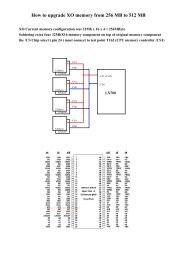
NAND Flash Memory MT29F4G08AAAWP ... - Micron
NAND Flash Memory MT29F4G08AAAWP ... - Micron
NAND Flash Memory MT29F4G08AAAWP ... - Micron
- No tags were found...

You also want an ePaper? Increase the reach of your titles
YUMPU automatically turns print PDFs into web optimized ePapers that Google loves.
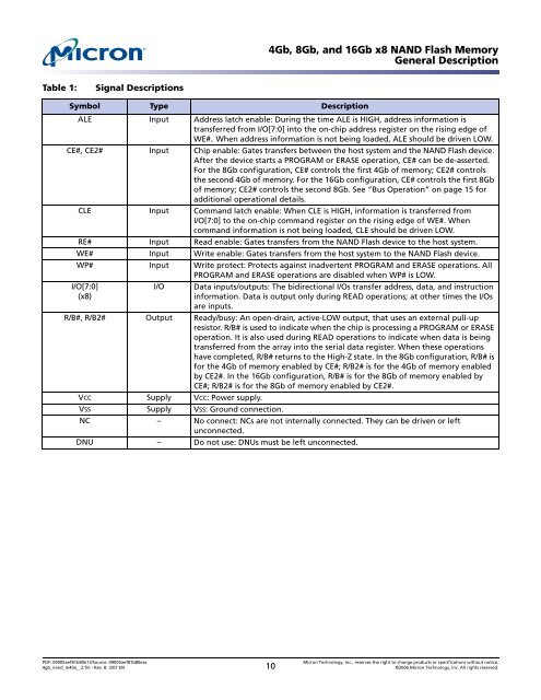
4Gb, 8Gb, and 16Gb x8 <strong>NAND</strong> <strong>Flash</strong> <strong>Memory</strong>General DescriptionTable 1:Signal DescriptionsSymbol Type DescriptionALE Input Address latch enable: During the time ALE is HIGH, address information istransferred from I/O[7:0] into the on-chip address register on the rising edge ofWE#. When address information is not being loaded, ALE should be driven LOW.CE#, CE2# Input Chip enable: Gates transfers between the host system and the <strong>NAND</strong> <strong>Flash</strong> device.After the device starts a PROGRAM or ERASE operation, CE# can be de-asserted.For the 8Gb configuration, CE# controls the first 4Gb of memory; CE2# controlsthe second 4Gb of memory. For the 16Gb configuration, CE# controls the first 8Gbof memory; CE2# controls the second 8Gb. See “Bus Operation” on page 15 foradditional operational details.CLE Input Command latch enable: When CLE is HIGH, information is transferred fromI/O[7:0] to the on-chip command register on the rising edge of WE#. Whencommand information is not being loaded, CLE should be driven LOW.RE# Input Read enable: Gates transfers from the <strong>NAND</strong> <strong>Flash</strong> device to the host system.WE# Input Write enable: Gates transfers from the host system to the <strong>NAND</strong> <strong>Flash</strong> device.WP# Input Write protect: Protects against inadvertent PROGRAM and ERASE operations. AllPROGRAM and ERASE operations are disabled when WP# is LOW.I/O[7:0](x8)I/O Data inputs/outputs: The bidirectional I/Os transfer address, data, and instructioninformation. Data is output only during READ operations; at other times the I/Osare inputs.R/B#, R/B2# Output Ready/busy: An open-drain, active-LOW output, that uses an external pull-upresistor. R/B# is used to indicate when the chip is processing a PROGRAM or ERASEoperation. It is also used during READ operations to indicate when data is beingtransferred from the array into the serial data register. When these operationshave completed, R/B# returns to the High-Z state. In the 8Gb configuration, R/B# isfor the 4Gb of memory enabled by CE#; R/B2# is for the 4Gb of memory enabledby CE2#. In the 16Gb configuration, R/B# is for the 8Gb of memory enabled byCE#; R/B2# is for the 8Gb of memory enabled by CE2#.VCC Supply VCC: Power supply.VSS Supply VSS: Ground connection.NC – No connect: NCs are not internally connected. They can be driven or leftunconnected.DNU – Do not use: DNUs must be left unconnected.PDF: 09005aef81b80e13/Source: 09005aef81b80eac<strong>Micron</strong> Technology, Inc., reserves the right to change products or specifications without notice.4gb_nand_m40a__2.fm - Rev. B 2/07 EN 10 ©2006 <strong>Micron</strong> Technology, Inc. All rights reserved.