NAND Flash Memory MT29F4G08AAAWP ... - Micron
NAND Flash Memory MT29F4G08AAAWP ... - Micron
NAND Flash Memory MT29F4G08AAAWP ... - Micron
- No tags were found...
You also want an ePaper? Increase the reach of your titles
YUMPU automatically turns print PDFs into web optimized ePapers that Google loves.
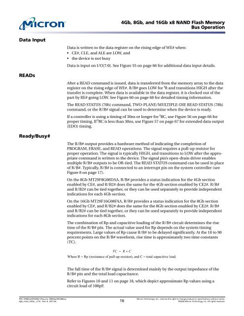
4Gb, 8Gb, and 16Gb x8 <strong>NAND</strong> <strong>Flash</strong> <strong>Memory</strong>Bus OperationData InputREADsReady/Busy#Data is written to the data register on the rising edge of WE# when:• CE#, CLE, and ALE are LOW, and• the device is not busyData is input on I/O[7:0]. See Figure 55 on page 66 for additional data input details.After a READ command is issued, data is transferred from the memory array to the dataregister on the rising edge of WE#. R/B# goes LOW for t R and transitions HIGH after thetransfer is complete. When data is available in the data register, it is clocked out of thepart by RE# going LOW. See Figure 60 on page 68 for detailed timing information.The READ STATUS (70h) command, TWO-PLANE/MULTIPLE-DIE READ STATUS (78h)command, or the R/B# signal can be used to determine when the device is ready.If a controller is using a timing of 30ns or longer for t RC, use Figure 56 on page 66 forproper timing. If t RC is less than 30ns, use Figure 57 on page 67 for extended data output(EDO) timing.The R/B# output provides a hardware method of indicating the completion ofPROGRAM, ERASE, and READ operations. The signal requires a pull-up resistor forproper operation. The signal is typically HIGH, and transitions to LOW after the appropriatecommand is written to the device. The signal pin’s open-drain driver enablesmultiple R/B# outputs to be OR-tied. The READ STATUS command can be used in placeof R/B#. Typically, R/B# is connected to an interrupt pin on the system controller (seeFigure 8 on page 17).On the 8Gb MT29F8G08DAA, R/B# provides a status indication for the 4Gb sectionenabled by CE#, and R/B2# does the same for the 4Gb section enabled by CE2#. R/B#and R/B2# can be tied together, or they can be used separately to provide independentindications for each 4Gb section.On the 16Gb MT29F16G08FAA, R/B# provides a status indication for the 8Gb sectionenabled by CE#, and R/B2# does the same for the 8Gb section enabled by CE2#. R/B#and R/B2# can be tied together, or they can be used separately to provide independentindications for each 8Gb section.The combination of Rp and capacitive loading of the R/B# circuit determines the risetime of the R/B# pin. The actual value used for Rp depends on the system timingrequirements. Large values of Rp cause R/B# to be delayed significantly. At the 10 to 90percent points on the R/B# waveform, rise time is approximately two time constants(TC).TC = R × CWhere R = Rp (resistance of pull-up resistor), and C = total capacitive load.The fall time of the R/B# signal is determined mainly by the output impedance of theR/B# pin and the total load capacitance.Refer to Figures 10 and 11 on page 18, which depict approximate Rp values using acircuit load of 100pF.PDF: 09005aef81b80e13/Source: 09005aef81b80eac<strong>Micron</strong> Technology, Inc., reserves the right to change products or specifications without notice.4gb_nand_m40a__2.fm - Rev. B 2/07 EN 16 ©2006 <strong>Micron</strong> Technology, Inc. All rights reserved.


