NAND Flash Memory MT29F4G08AAAWP ... - Micron
NAND Flash Memory MT29F4G08AAAWP ... - Micron
NAND Flash Memory MT29F4G08AAAWP ... - Micron
- No tags were found...

You also want an ePaper? Increase the reach of your titles
YUMPU automatically turns print PDFs into web optimized ePapers that Google loves.
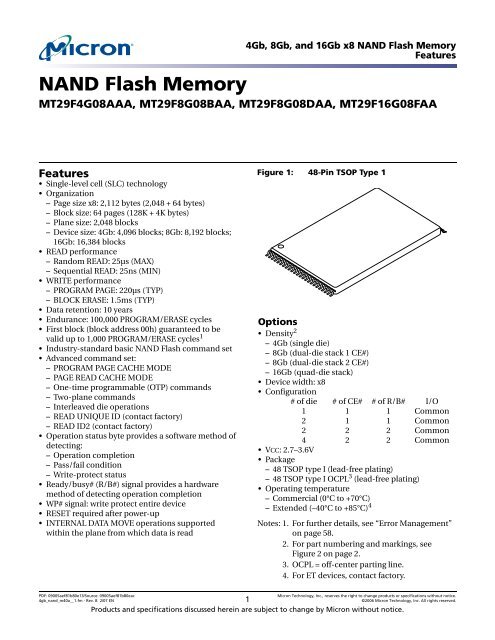
4Gb, 8Gb, and 16Gb x8 <strong>NAND</strong> <strong>Flash</strong> <strong>Memory</strong>Features<strong>NAND</strong> <strong>Flash</strong> <strong>Memory</strong>MT29F4G08AAA, MT29F8G08BAA, MT29F8G08DAA, MT29F16G08FAAFeatures• Single-level cell (SLC) technology• Organization– Page size x8: 2,112 bytes (2,048 + 64 bytes)– Block size: 64 pages (128K + 4K bytes)– Plane size: 2,048 blocks– Device size: 4Gb: 4,096 blocks; 8Gb: 8,192 blocks;16Gb: 16,384 blocks• READ performance– Random READ: 25µs (MAX)– Sequential READ: 25ns (MIN)• WRITE performance– PROGRAM PAGE: 220µs (TYP)– BLOCK ERASE: 1.5ms (TYP)• Data retention: 10 years• Endurance: 100,000 PROGRAM/ERASE cycles• First block (block address 00h) guaranteed to bevalid up to 1,000 PROGRAM/ERASE cycles 1• Industry-standard basic <strong>NAND</strong> <strong>Flash</strong> command set• Advanced command set:– PROGRAM PAGE CACHE MODE– PAGE READ CACHE MODE– One-time programmable (OTP) commands– Two-plane commands– Interleaved die operations– READ UNIQUE ID (contact factory)– READ ID2 (contact factory)• Operation status byte provides a software method ofdetecting:– Operation completion– Pass/fail condition– Write-protect status• Ready/busy# (R/B#) signal provides a hardwaremethod of detecting operation completion• WP# signal: write protect entire device• RESET required after power-up• INTERNAL DATA MOVE operations supportedwithin the plane from which data is readFigure 1: 48-Pin TSOP Type 1Options• Density 2– 4Gb (single die)– 8Gb (dual-die stack 1 CE#)– 8Gb (dual-die stack 2 CE#)– 16Gb (quad-die stack)• Device width: x8• Configuration# of die # of CE# # of R/B# I/O1 1 1 Common2 1 1 Common2 2 2 Common4 2 2 Common• VCC: 2.7–3.6V• Package– 48 TSOP type I (lead-free plating)– 48 TSOP type I OCPL 3 (lead-free plating)• Operating temperature– Commercial (0°C to +70°C)– Extended (–40°C to +85°C) 4Notes: 1. For further details, see “Error Management”on page 58.2. For part numbering and markings, seeFigure 2 on page 2.3. OCPL = off-center parting line.4. For ET devices, contact factory.PDF: 09005aef81b80e13/Source: 09005aef81b80eac<strong>Micron</strong> Technology, Inc., reserves the right to change products or specifications without notice.4gb_nand_m40a__1.fm - Rev. B 2/07 EN 1 ©2006 <strong>Micron</strong> Technology, Inc. All rights reserved.Products and specifications discussed herein are subject to change by <strong>Micron</strong> without notice.
Part Numbering Information4Gb, 8Gb, and 16Gb x8 <strong>NAND</strong> <strong>Flash</strong> <strong>Memory</strong>Part Numbering Information<strong>Micron</strong> ® <strong>NAND</strong> <strong>Flash</strong> devices are available in several different configurations anddensities (see Figure 2).Figure 2:Part Number ChartMT 29F 4G 08 A A A WP ES :A<strong>Micron</strong> TechnologyProduct Family29F = Single-Supply <strong>NAND</strong> <strong>Flash</strong> <strong>Memory</strong>Density4G = 4Gb8G = 8Gb16G = 16GbDevice Width08 = 8 bitsClassification# of die # of CE# # of R/B# I/OA 1 1 1 CommonB 2 1 1 CommonD 2 2 2 CommonF 4 2 2 CommonOperating Voltage RangeA = 3.3V (2.70–3.60V)Design RevisionA = First RevisionProduction StatusBlank = ProductionES = Engineering SampleMS = Mechanical SampleQS = Qualification SampleOperating Temperature RangeBlank = Commercial (0°C to +70°C)ET = Extended 1 (-40°C to +85°C)Reserved for Future UseBlank<strong>Flash</strong> PerformanceBlank = StandardPackage CodeWP = 48-pin TSOP I (lead-free)WC = 48-pin TSOP I OCPL (lead-free)Feature SetA = Feature Set ANotes:1. For ET devices, contact factory.Valid Part Number CombinationsAfter building the part number from the part numbering chart, verify that the partnumber is offered and valid by using the <strong>Micron</strong> Parametric Part Search Web site atwww.micron.com/products/parametric. If the device required is not on this list, contactthe factory.PDF: 09005aef81b80e13/Source: 09005aef81b80eac<strong>Micron</strong> Technology, Inc., reserves the right to change products or specifications without notice.4gb_nand_m40a__1.fm - Rev. B 2/07 EN 2 ©2006 <strong>Micron</strong> Technology, Inc. All rights reserved.
4Gb, 8Gb, and 16Gb x8 <strong>NAND</strong> <strong>Flash</strong> <strong>Memory</strong>Table of ContentsWRITE PROTECT Operation . . . . . . . . . . . . . . . . . . . . . . . . . . . . . . . . . . . . . . . . . . . . . . . . . . . . . . . . . . . . . . . . . . . . . . . .57Error Management . . . . . . . . . . . . . . . . . . . . . . . . . . . . . . . . . . . . . . . . . . . . . . . . . . . . . . . . . . . . . . . . . . . . . . . . . . . . . . . . . . .58Electrical Characteristics . . . . . . . . . . . . . . . . . . . . . . . . . . . . . . . . . . . . . . . . . . . . . . . . . . . . . . . . . . . . . . . . . . . . . . . . . . . . . .59VCC Power Cycling . . . . . . . . . . . . . . . . . . . . . . . . . . . . . . . . . . . . . . . . . . . . . . . . . . . . . . . . . . . . . . . . . . . . . . . . . . . . . . . . .60Timing Diagrams. . . . . . . . . . . . . . . . . . . . . . . . . . . . . . . . . . . . . . . . . . . . . . . . . . . . . . . . . . . . . . . . . . . . . . . . . . . . . . . . . . . . .65Package Dimensions . . . . . . . . . . . . . . . . . . . . . . . . . . . . . . . . . . . . . . . . . . . . . . . . . . . . . . . . . . . . . . . . . . . . . . . . . . . . . . . . .79PDF: 09005aef81b80e13/Source: 09005aef81b80eac<strong>Micron</strong> Technology, Inc., reserves the right to change products or specifications without notice.4gb_nand_m40aTOC.fm - Rev. B 2/07 EN 4 ©2006 <strong>Micron</strong> Technology, Inc. All rights reserved.
4Gb, 8Gb, and 16Gb x8 <strong>NAND</strong> <strong>Flash</strong> <strong>Memory</strong>List of FiguresFigure 56: SERIAL ACCESS Cycle After READ . . . . . . . . . . . . . . . . . . . . . . . . . . . . . . . . . . . . . . . . . . . . . . . . . . . . . . . . .66Figure 57: SERIAL ACCESS Cycle After READ (EDO Mode) . . . . . . . . . . . . . . . . . . . . . . . . . . . . . . . . . . . . . . . . . . . . .67Figure 58: READ STATUS Operation . . . . . . . . . . . . . . . . . . . . . . . . . . . . . . . . . . . . . . . . . . . . . . . . . . . . . . . . . . . . . . . . .67Figure 59: TWO-PLANE/MULTIPLE-DIE READ STATUS Operation . . . . . . . . . . . . . . . . . . . . . . . . . . . . . . . . . . . . .68Figure 60: PAGE READ Operation . . . . . . . . . . . . . . . . . . . . . . . . . . . . . . . . . . . . . . . . . . . . . . . . . . . . . . . . . . . . . . . . . . .68Figure 61: READ Operation with CE# “Don’t Care” . . . . . . . . . . . . . . . . . . . . . . . . . . . . . . . . . . . . . . . . . . . . . . . . . . . .69Figure 62: RANDOM DATA READ Operation . . . . . . . . . . . . . . . . . . . . . . . . . . . . . . . . . . . . . . . . . . . . . . . . . . . . . . . . .69Figure 63: PAGE READ CACHE MODE Operation, Part 1 of 2 . . . . . . . . . . . . . . . . . . . . . . . . . . . . . . . . . . . . . . . . . . .70Figure 64: PAGE READ CACHE MODE Operation, Part 2 of 2 . . . . . . . . . . . . . . . . . . . . . . . . . . . . . . . . . . . . . . . . . . .71Figure 65: PAGE READ CACHE MODE Operation without R/B#, Part 1 of 2 . . . . . . . . . . . . . . . . . . . . . . . . . . . . . .72Figure 66: PAGE READ CACHE MODE Operation without R/B#, Part 2 of 2 . . . . . . . . . . . . . . . . . . . . . . . . . . . . . .73Figure 67: READ ID Operation . . . . . . . . . . . . . . . . . . . . . . . . . . . . . . . . . . . . . . . . . . . . . . . . . . . . . . . . . . . . . . . . . . . . . .74Figure 68: PROGRAM PAGE Operation. . . . . . . . . . . . . . . . . . . . . . . . . . . . . . . . . . . . . . . . . . . . . . . . . . . . . . . . . . . . . . .74Figure 69: Program Operation with CE# “Don’t Care” . . . . . . . . . . . . . . . . . . . . . . . . . . . . . . . . . . . . . . . . . . . . . . . . .75Figure 70: PROGRAM PAGE Operation with RANDOM DATA INPUT. . . . . . . . . . . . . . . . . . . . . . . . . . . . . . . . . . . .75Figure 71: INTERNAL DATA MOVE Operation . . . . . . . . . . . . . . . . . . . . . . . . . . . . . . . . . . . . . . . . . . . . . . . . . . . . . . . .76Figure 72: PROGRAM PAGE CACHE MODE Operation. . . . . . . . . . . . . . . . . . . . . . . . . . . . . . . . . . . . . . . . . . . . . . . . .76Figure 73: PROGRAM PAGE CACHE MODE Operation Ending on 15h. . . . . . . . . . . . . . . . . . . . . . . . . . . . . . . . . . .77Figure 74: BLOCK ERASE Operation . . . . . . . . . . . . . . . . . . . . . . . . . . . . . . . . . . . . . . . . . . . . . . . . . . . . . . . . . . . . . . . . .78Figure 75: RESET Operation . . . . . . . . . . . . . . . . . . . . . . . . . . . . . . . . . . . . . . . . . . . . . . . . . . . . . . . . . . . . . . . . . . . . . . . .78Figure 76: 48-Pin TSOP Type 1 (WP Package Code) . . . . . . . . . . . . . . . . . . . . . . . . . . . . . . . . . . . . . . . . . . . . . . . . . . . .79Figure 77: 48-Pin TSOP OCPL Type 1 (WC Package Code) . . . . . . . . . . . . . . . . . . . . . . . . . . . . . . . . . . . . . . . . . . . . . .80PDF: 09005aef81b80e13/Source: 09005aef81b80eac<strong>Micron</strong> Technology, Inc., reserves the right to change products or specifications without notice.4gb_nand_m40aLOF.fm - Rev. B 2/07 EN 6 ©2006 <strong>Micron</strong> Technology, Inc. All rights reserved.
List of Tables4Gb, 8Gb, and 16Gb x8 <strong>NAND</strong> <strong>Flash</strong> <strong>Memory</strong>List of TablesTable 1: Signal Descriptions. . . . . . . . . . . . . . . . . . . . . . . . . . . . . . . . . . . . . . . . . . . . . . . . . . . . . . . . . . . . . . . . . . . . . . .10Table 2: Operational Example . . . . . . . . . . . . . . . . . . . . . . . . . . . . . . . . . . . . . . . . . . . . . . . . . . . . . . . . . . . . . . . . . . . . .12Table 3: Array Addressing: MT29F4G08AAA and MT29F8G08DAA. . . . . . . . . . . . . . . . . . . . . . . . . . . . . . . . . . . . .13Table 4: Array Addressing: MT28F8G08BAA and MT29F16G08FAA . . . . . . . . . . . . . . . . . . . . . . . . . . . . . . . . . . . .14Table 5: Mode Selection . . . . . . . . . . . . . . . . . . . . . . . . . . . . . . . . . . . . . . . . . . . . . . . . . . . . . . . . . . . . . . . . . . . . . . . . . .18Table 6: Command Set . . . . . . . . . . . . . . . . . . . . . . . . . . . . . . . . . . . . . . . . . . . . . . . . . . . . . . . . . . . . . . . . . . . . . . . . . . .19Table 7: Two-Plane Command Set . . . . . . . . . . . . . . . . . . . . . . . . . . . . . . . . . . . . . . . . . . . . . . . . . . . . . . . . . . . . . . . . .20Table 8: Device ID and Configuration Codes. . . . . . . . . . . . . . . . . . . . . . . . . . . . . . . . . . . . . . . . . . . . . . . . . . . . . . . .25Table 9: Status Register Bit Definition . . . . . . . . . . . . . . . . . . . . . . . . . . . . . . . . . . . . . . . . . . . . . . . . . . . . . . . . . . . . . .26Table 10: Status Register Contents After RESET Operation . . . . . . . . . . . . . . . . . . . . . . . . . . . . . . . . . . . . . . . . . . . .56Table 11: Absolute Maximum Ratings . . . . . . . . . . . . . . . . . . . . . . . . . . . . . . . . . . . . . . . . . . . . . . . . . . . . . . . . . . . . . . .59Table 12: Recommended Operating Conditions . . . . . . . . . . . . . . . . . . . . . . . . . . . . . . . . . . . . . . . . . . . . . . . . . . . . . .59Table 13: M29FxGxxxAA 3V Device DC and Operating Characteristics . . . . . . . . . . . . . . . . . . . . . . . . . . . . . . . . . .61Table 14: Valid Blocks . . . . . . . . . . . . . . . . . . . . . . . . . . . . . . . . . . . . . . . . . . . . . . . . . . . . . . . . . . . . . . . . . . . . . . . . . . . . .61Table 15: Capacitance . . . . . . . . . . . . . . . . . . . . . . . . . . . . . . . . . . . . . . . . . . . . . . . . . . . . . . . . . . . . . . . . . . . . . . . . . . . . .62Table 16: Test Conditions . . . . . . . . . . . . . . . . . . . . . . . . . . . . . . . . . . . . . . . . . . . . . . . . . . . . . . . . . . . . . . . . . . . . . . . . . .62Table 17: AC Characteristics: Command, Data, and Address Input . . . . . . . . . . . . . . . . . . . . . . . . . . . . . . . . . . . . .62Table 18: AC Characteristics: Normal Operation. . . . . . . . . . . . . . . . . . . . . . . . . . . . . . . . . . . . . . . . . . . . . . . . . . . . . .63Table 19: PROGRAM/ERASE Characteristics . . . . . . . . . . . . . . . . . . . . . . . . . . . . . . . . . . . . . . . . . . . . . . . . . . . . . . . . .64PDF: 09005aef81b80e13/Source: 09005aef81b80eac<strong>Micron</strong> Technology, Inc., reserves the right to change products or specifications without notice.4gb_nand_m40aLOT.fm - Rev. B 2/07 EN 7 ©2006 <strong>Micron</strong> Technology, Inc. All rights reserved.
General Description4Gb, 8Gb, and 16Gb x8 <strong>NAND</strong> <strong>Flash</strong> <strong>Memory</strong>General Description<strong>NAND</strong> <strong>Flash</strong> technology provides a cost-effective solution for applications requiringhigh-density, solid-state storage. The MT29F4G08AAA is a 4Gb <strong>NAND</strong> <strong>Flash</strong> memorydevice. The MT29F8G08BAA is a two-die stack that operates as a single 8Gb device. TheMT29F8G08DAA is a two-die stack that operates as two independent 4Gb devices. TheMT29F16G08FAA is a four-die stack that operates as two independent 8Gb devices,providing a total storage capacity of 16Gb in a single, space-saving package. <strong>Micron</strong><strong>NAND</strong> <strong>Flash</strong> devices include standard <strong>NAND</strong> <strong>Flash</strong> features as well as new featuresdesigned to enhance system-level performance.<strong>Micron</strong> <strong>NAND</strong> <strong>Flash</strong> devices use a highly multiplexed 8-bit bus (I/O[7:0]) to transferdata, addresses, and instructions. The five command pins (CLE, ALE, CE#, RE#, WE#)implement the <strong>NAND</strong> <strong>Flash</strong> command bus interface protocol. Additional pins controlhardware write protection (WP#) and monitor device status (R/B#).This hardware interface creates a low-pin-count device with a standard pinout that isthe same from one density to another, allowing future upgrades to higher densitieswithout board redesign.The MT29F4G, MT29F8G, and MT29F16G devices contain two planes per die. Eachplane consists of 2,048 blocks. Each block is subdivided into 64 programmable pages.Each page consists of 2,112 bytes. The pages are further divided into a 2,048-byte datastorage region with a separate 64-byte area. The 64-byte area is typically used for errormanagement functions.The contents of each page can be programmed in 220µs (TYP), and an entire block canbe erased in 1.5ms (TYP). On-chip control logic automates PROGRAM and ERASE operationsto maximize cycle endurance. PROGRAM/ERASE endurance is specified at100,000 cycles with appropriate error correction code (ECC) and error management.PDF: 09005aef81b80e13/Source: 09005aef81b80eac<strong>Micron</strong> Technology, Inc., reserves the right to change products or specifications without notice.4gb_nand_m40a__2.fm - Rev. B 2/07 EN 8 ©2006 <strong>Micron</strong> Technology, Inc. All rights reserved.
4Gb, 8Gb, and 16Gb x8 <strong>NAND</strong> <strong>Flash</strong> <strong>Memory</strong>General DescriptionFigure 3:48-Pin TSOP Type 1 Pin Assignment (Top View)Notes:x8NCNCNCNCNCR/B2# 1R/B#RE#CE#CE2# 1NCVccVssNCNCCLEALEWE#WP#NCNCNCNCNC1234567891011121314151617181920212223241. CE2# and R/B2# are available on 8Gb 2-CE# devices and 16Gb devices only. These pins areNC for other configurations.484746454443424140393837363534333231302928272625x8DNUNCNCNCI/O7I/O6I/O5I/O4NCNCDNU or VssVccVssNCNCNCI/O3I/O2I/O1I/O0NCNCDNUDNUPDF: 09005aef81b80e13/Source: 09005aef81b80eac<strong>Micron</strong> Technology, Inc., reserves the right to change products or specifications without notice.4gb_nand_m40a__2.fm - Rev. B 2/07 EN 9 ©2006 <strong>Micron</strong> Technology, Inc. All rights reserved.
4Gb, 8Gb, and 16Gb x8 <strong>NAND</strong> <strong>Flash</strong> <strong>Memory</strong>General DescriptionTable 1:Signal DescriptionsSymbol Type DescriptionALE Input Address latch enable: During the time ALE is HIGH, address information istransferred from I/O[7:0] into the on-chip address register on the rising edge ofWE#. When address information is not being loaded, ALE should be driven LOW.CE#, CE2# Input Chip enable: Gates transfers between the host system and the <strong>NAND</strong> <strong>Flash</strong> device.After the device starts a PROGRAM or ERASE operation, CE# can be de-asserted.For the 8Gb configuration, CE# controls the first 4Gb of memory; CE2# controlsthe second 4Gb of memory. For the 16Gb configuration, CE# controls the first 8Gbof memory; CE2# controls the second 8Gb. See “Bus Operation” on page 15 foradditional operational details.CLE Input Command latch enable: When CLE is HIGH, information is transferred fromI/O[7:0] to the on-chip command register on the rising edge of WE#. Whencommand information is not being loaded, CLE should be driven LOW.RE# Input Read enable: Gates transfers from the <strong>NAND</strong> <strong>Flash</strong> device to the host system.WE# Input Write enable: Gates transfers from the host system to the <strong>NAND</strong> <strong>Flash</strong> device.WP# Input Write protect: Protects against inadvertent PROGRAM and ERASE operations. AllPROGRAM and ERASE operations are disabled when WP# is LOW.I/O[7:0](x8)I/O Data inputs/outputs: The bidirectional I/Os transfer address, data, and instructioninformation. Data is output only during READ operations; at other times the I/Osare inputs.R/B#, R/B2# Output Ready/busy: An open-drain, active-LOW output, that uses an external pull-upresistor. R/B# is used to indicate when the chip is processing a PROGRAM or ERASEoperation. It is also used during READ operations to indicate when data is beingtransferred from the array into the serial data register. When these operationshave completed, R/B# returns to the High-Z state. In the 8Gb configuration, R/B# isfor the 4Gb of memory enabled by CE#; R/B2# is for the 4Gb of memory enabledby CE2#. In the 16Gb configuration, R/B# is for the 8Gb of memory enabled byCE#; R/B2# is for the 8Gb of memory enabled by CE2#.VCC Supply VCC: Power supply.VSS Supply VSS: Ground connection.NC – No connect: NCs are not internally connected. They can be driven or leftunconnected.DNU – Do not use: DNUs must be left unconnected.PDF: 09005aef81b80e13/Source: 09005aef81b80eac<strong>Micron</strong> Technology, Inc., reserves the right to change products or specifications without notice.4gb_nand_m40a__2.fm - Rev. B 2/07 EN 10 ©2006 <strong>Micron</strong> Technology, Inc. All rights reserved.
4Gb, 8Gb, and 16Gb x8 <strong>NAND</strong> <strong>Flash</strong> <strong>Memory</strong>ArchitectureArchitectureThese devices use <strong>NAND</strong> <strong>Flash</strong> electrical and command interfaces. Data, commands,and addresses are multiplexed onto the same pins and received by I/O control circuits.This provides a memory device with a low pin count. The commands received at the I/Ocontrol circuits are latched by a command register and are transferred to control logiccircuits for generating internal signals to control device operations. The addresses arelatched by an address register and sent to a row decoder or a column decoder to select arow address or a column address, respectively.The data are transferred to or from the <strong>NAND</strong> <strong>Flash</strong> memory array, byte by byte (x8),through a data register and a cache register. The cache register is closest to I/O controlcircuits and acts as a data buffer for the I/O data, whereas the data register is closest tothe memory array and acts as a data buffer for the <strong>NAND</strong> <strong>Flash</strong> memory array operation.The <strong>NAND</strong> <strong>Flash</strong> memory array is programmed and read in page-based operations andis erased in block-based operations. During normal page operations, the data and cacheregisters are tied together and act as a single register. During cache operations the dataand cache registers operate independently to increase data throughput.These devices also have a status register that reports the status of device operation.Figure 4:<strong>NAND</strong> <strong>Flash</strong> Functional Block DiagramVCCVSSI/OxI/OControlAddress RegisterStatus RegisterCommand RegisterCE#CLEALEWE#RE#WP#ControlLogicRow DecodeColumn Decode<strong>NAND</strong> <strong>Flash</strong>Array(2 planes)R/B#Data RegisterCache RegisterPDF: 09005aef81b80e13/Source: 09005aef81b80eac<strong>Micron</strong> Technology, Inc., reserves the right to change products or specifications without notice.4gb_nand_m40a__2.fm - Rev. B 2/07 EN 11 ©2006 <strong>Micron</strong> Technology, Inc. All rights reserved.
4Gb, 8Gb, and 16Gb x8 <strong>NAND</strong> <strong>Flash</strong> <strong>Memory</strong>AddressingAddressing<strong>NAND</strong> <strong>Flash</strong> devices do not contain dedicated address pins. Addresses are loaded usinga 5-cycle sequence as shown in Tables 3 and 4, on pages 13 and 14. See Figure 5 for additionalmemory mapping and addressing details.<strong>Memory</strong> MappingFigure 5:<strong>Memory</strong> MapBlocks4Gb, 8Gb 2 CE#: BA[17:6]8Gb 1 CE#, 16Gb: BA[18:6]0 1 2• • • • • • • • • • • •4,0958Gb 2 CE#: 4,096 blocks per CE#8Gb 1 CE#: 8,192 blocks per CE#16Gb: 8,192 blocks per CE#PagesPA[5:0]0 1 2 • • • 63BytesCA[11:0]0 1 2 • • • • • • • • • • • • • • • • • • • 2,047 • • • 2,111Spare areaTable 2:Operational ExampleBlock Page Min Address in Page Max Address in Page Out of Bounds Addresses in Page0 0 0x0000000000 0x000000083F 0x0000000840–0x0000000FFF0 1 0x0000010000 0x000001083F 0x0000010840–0x0000010FFF0 2 0x0000020000 0x000002083F 0x0000020840–0x0000020FFF… … … …4,095 62 0x03FFFE0000 0x03FFFE083F 0x03FFFE0840–0x03FFFE0FFF4,095 63 0x03FFFF0000 0x03FFFF083F 0x03FFFF0840–0x03FFFF0FFFNotes:1. As shown in Table 3 on page 13, the high nibble of ADDRESS cycle 2 has no assignedaddress bits; however, these 4 bits must be held LOW during the ADDRESS cycle to ensurethat the address is interpreted correctly by the <strong>NAND</strong> <strong>Flash</strong> device. These extra bits areaccounted for in ADDRESS cycle 2 even though they do not have address bits assigned tothem.2. The 12-bit column address is capable of addressing from 0 to 4,095 bytes on a x8 device;however, only bytes 0 through 2,111 are valid. Bytes 2,112 through 4,095 of each page are“out of bounds,” do not exist in the device, and cannot be addressed.PDF: 09005aef81b80e13/Source: 09005aef81b80eac<strong>Micron</strong> Technology, Inc., reserves the right to change products or specifications without notice.4gb_nand_m40a__2.fm - Rev. B 2/07 EN 12 ©2006 <strong>Micron</strong> Technology, Inc. All rights reserved.
4Gb, 8Gb, and 16Gb x8 <strong>NAND</strong> <strong>Flash</strong> <strong>Memory</strong>Array OrganizationArray OrganizationFigure 6:Array Organization for MT29F4G08AAA and MT29F8G08DAA (x8)Cache Register2,0482,112 bytes642,0482,112 bytes64I/O0I/O7Data Register2,048 642,048642,048 blocksper plane4,096 blocksper device1 block 1 block1 page = (2K + 64 bytes)1 block = (2K + 64) bytes x 64 pages= (128K + 4K) bytes1 plane = (128K + 4K) bytes x 2,048 blocks= 2,112Mb1 device = 2,112Mb x 2 planes= 4,224MbPlane ofeven-numbered blocks(0, 2, 4, 6, ..., 4,092, 4,094)Plane ofodd-numbered blocks(1, 3, 5, 7, ..., 4,093, 4,095)Notes:1. For the 8Gb MT29F8G08DAA, the 4Gb array organization shown applies to each chip enable(CE# and CE2#).Table 3:Array Addressing: MT29F4G08AAA and MT29F8G08DAACycle I/O7 I/O6 I/O5 I/O4 I/O3 I/O2 I/O1 I/O0First CA7 CA6 CA5 CA4 CA3 CA2 CA1 CA0Second LOW LOW LOW LOW CA11 CA10 CA9 CA8Third BA7 BA6 PA5 PA4 PA3 PA2 PA1 PA0Fourth BA15 BA14 BA13 BA12 BA11 BA10 BA9 BA8Fifth LOW LOW LOW LOW LOW LOW BA17 BA16Notes:1. Block address concatenated with page address = actual page address. CAx = columnaddress; PAx = page address; BAx = block address.2. If CA11 is “1,” then CA[10:6] must be “0.”PDF: 09005aef81b80e13/Source: 09005aef81b80eac<strong>Micron</strong> Technology, Inc., reserves the right to change products or specifications without notice.4gb_nand_m40a__2.fm - Rev. B 2/07 EN 13 ©2006 <strong>Micron</strong> Technology, Inc. All rights reserved.
4Gb, 8Gb, and 16Gb x8 <strong>NAND</strong> <strong>Flash</strong> <strong>Memory</strong>Array OrganizationFigure 7:Array Organization for MT29F8G08BAA and MT29F16G08FAA (x8)Die 0 Die 1Cache Register2,0482,112 bytes642,0482,112 bytes642,0482,112 bytes642,0482,112 bytes64I/O0I/O7Data Register2,048 642,048642,048 642,048641 page = (2K + 64 bytes)2,048 blocksper plane4,096 blocksper die1 block 1 block1 block 1 block1 block = (2K + 64) bytes x 64 pages= (128K + 4K) bytes1 plane = (128K + 4K) bytes x 2,048 blocks= 2,112Mb1 die = 2,112Mb x 2 planes= 4,224MbPlane 0: evennumberedblocks numbered blocksPlane 1: odd-(0, 2, 4, 6, ..., (1, 3, 5, 7, ...,4,092, 4,094) 1 4,093, 4,095)Plane 0: evennumberedblocks(4,096, 4,098, ...,8,188, 8,190)Plane 1: oddnumberedblocks(4,097,4,099, ...,8,189, 8,191)1 device = 4,224Mb x 2 die= 8,448MbNotes: 1. Die 0, Plane 0: BA18 = 0; BA6 = 0.Die 0, Plane 1: BA18 = 0; BA6 = 1.Die 1, Plane 0: BA18 = 1; BA6 = 0.Die 1, Plane 1: BA18 = 1; BA6 = 1.2. For the 16Gb MT29F16G08FAA, the 8Gb array organization shown here applies to each chipenable (CE# and CE2#).Table 4:Array Addressing: MT28F8G08BAA and MT29F16G08FAACycle I/O7 I/O6 I/O5 I/O4 I/O3 I/O2 I/O1 I/O0First CA7 CA6 CA5 CA4 CA3 CA2 CA1 CA0Second LOW LOW LOW LOW CA11 CA10 CA9 CA8Third BA7 BA6 PA5 PA4 PA3 PA2 PA1 PA0Fourth BA15 BA14 BA13 BA12 BA11 BA10 BA9 BA8Fifth LOW LOW LOW LOW LOW BA18 3 BA17 BA16Notes:1. CAx = column address; PAx = page address; BAx = block address.2. If CA11 is 1, then CA[10:6] must be “0.”3. Die address boundary: 0 = 0–4Gb; 1 = 4Gb–8Gb.PDF: 09005aef81b80e13/Source: 09005aef81b80eac<strong>Micron</strong> Technology, Inc., reserves the right to change products or specifications without notice.4gb_nand_m40a__2.fm - Rev. B 2/07 EN 14 ©2006 <strong>Micron</strong> Technology, Inc. All rights reserved.
4Gb, 8Gb, and 16Gb x8 <strong>NAND</strong> <strong>Flash</strong> <strong>Memory</strong>Bus OperationBus OperationControl SignalsCommandsAddress InputThe bus on MT29Fxxx devices is multiplexed. Data I/O, addresses, and commands allshare the same pins, I/O[7:0].The command sequence normally consists of a COMMAND LATCH cycle, ADDRESSINPUT cycles, and 1 or more DATA cycles—either READ or WRITE.CE#, WE#, RE#, CLE, ALE, and WP# control <strong>NAND</strong> <strong>Flash</strong> device READ and WRITE operations.On the 8Gb MT29F8G08DAA, CE# and CE2# each control independent 4Gb arrays.On the 16Gb MT29F16G08FAA, CE# and CE2# each control independent 8Gb arrays.CE2# functions the same as CE# for its own array; all operations described for CE# alsoapply to CE2#.CE# is used to enable the device. When CE# is LOW and the device is not in the busystate, the <strong>NAND</strong> <strong>Flash</strong> memory will accept command, address, and data information.When the device is not performing an operation, the CE# pin is typically driven HIGHand the device enters standby mode. The memory will enter standby if CE# goes HIGHwhile data is being transferred and the device is not busy. This helps reduce powerconsumption. See Figure 61 on page 69 and Figure 69 on page 75 for examples of CE#“Don’t Care” operations.The CE# “Don’t Care” operation enables the <strong>NAND</strong> <strong>Flash</strong> to reside on the same asynchronousmemory bus as other <strong>Flash</strong> or SRAM devices. Other devices on the memorybus can then be accessed while the <strong>NAND</strong> <strong>Flash</strong> is busy with internal operations. Thiscapability is important for designs that require multiple <strong>NAND</strong> <strong>Flash</strong> devices on thesame bus.A HIGH CLE signal indicates that a command cycle is taking place. A HIGH ALE signalsignifies that an ADDRESS INPUT cycle is occurring.Commands are written to the command register on the rising edge of WE# when:• CE# and ALE are LOW, and• CLE is HIGH, and• The device is not busyAs exceptions, the device accepts the READ STATUS, TWO-PLANE/MULTIPLE-DIEREAD STATUS, and RESET commands when busy. Commands are transferred to thecommand register on the rising edge of WE# (see Figure 53 on page 65). Commands areinput on I/O[7:0].Addresses are written to the address register on the rising edge of WE# when:• CE# and CLE are LOW, and• ALE is HIGHAddresses are input on I/O[7:0]. Bits not part of the address space must be LOW.The number of ADDRESS cycles required for each command varies. Refer to thecommand descriptions to determine addressing requirements (see Table 6 on page 19).PDF: 09005aef81b80e13/Source: 09005aef81b80eac<strong>Micron</strong> Technology, Inc., reserves the right to change products or specifications without notice.4gb_nand_m40a__2.fm - Rev. B 2/07 EN 15 ©2006 <strong>Micron</strong> Technology, Inc. All rights reserved.
4Gb, 8Gb, and 16Gb x8 <strong>NAND</strong> <strong>Flash</strong> <strong>Memory</strong>Bus OperationData InputREADsReady/Busy#Data is written to the data register on the rising edge of WE# when:• CE#, CLE, and ALE are LOW, and• the device is not busyData is input on I/O[7:0]. See Figure 55 on page 66 for additional data input details.After a READ command is issued, data is transferred from the memory array to the dataregister on the rising edge of WE#. R/B# goes LOW for t R and transitions HIGH after thetransfer is complete. When data is available in the data register, it is clocked out of thepart by RE# going LOW. See Figure 60 on page 68 for detailed timing information.The READ STATUS (70h) command, TWO-PLANE/MULTIPLE-DIE READ STATUS (78h)command, or the R/B# signal can be used to determine when the device is ready.If a controller is using a timing of 30ns or longer for t RC, use Figure 56 on page 66 forproper timing. If t RC is less than 30ns, use Figure 57 on page 67 for extended data output(EDO) timing.The R/B# output provides a hardware method of indicating the completion ofPROGRAM, ERASE, and READ operations. The signal requires a pull-up resistor forproper operation. The signal is typically HIGH, and transitions to LOW after the appropriatecommand is written to the device. The signal pin’s open-drain driver enablesmultiple R/B# outputs to be OR-tied. The READ STATUS command can be used in placeof R/B#. Typically, R/B# is connected to an interrupt pin on the system controller (seeFigure 8 on page 17).On the 8Gb MT29F8G08DAA, R/B# provides a status indication for the 4Gb sectionenabled by CE#, and R/B2# does the same for the 4Gb section enabled by CE2#. R/B#and R/B2# can be tied together, or they can be used separately to provide independentindications for each 4Gb section.On the 16Gb MT29F16G08FAA, R/B# provides a status indication for the 8Gb sectionenabled by CE#, and R/B2# does the same for the 8Gb section enabled by CE2#. R/B#and R/B2# can be tied together, or they can be used separately to provide independentindications for each 8Gb section.The combination of Rp and capacitive loading of the R/B# circuit determines the risetime of the R/B# pin. The actual value used for Rp depends on the system timingrequirements. Large values of Rp cause R/B# to be delayed significantly. At the 10 to 90percent points on the R/B# waveform, rise time is approximately two time constants(TC).TC = R × CWhere R = Rp (resistance of pull-up resistor), and C = total capacitive load.The fall time of the R/B# signal is determined mainly by the output impedance of theR/B# pin and the total load capacitance.Refer to Figures 10 and 11 on page 18, which depict approximate Rp values using acircuit load of 100pF.PDF: 09005aef81b80e13/Source: 09005aef81b80eac<strong>Micron</strong> Technology, Inc., reserves the right to change products or specifications without notice.4gb_nand_m40a__2.fm - Rev. B 2/07 EN 16 ©2006 <strong>Micron</strong> Technology, Inc. All rights reserved.
4Gb, 8Gb, and 16Gb x8 <strong>NAND</strong> <strong>Flash</strong> <strong>Memory</strong>Bus OperationThe minimum value for Rp is determined by the output drive capability of the R/B#signal, the output voltage swing, and VCC.VCCRp( MIN , 3.3V part)( MAX) VOL= ---------------------------------------------------------------– ( MAX)= -------------------------3.2VIOL + ΣIL 8mA + ΣILWhere ΣIL is the sum of the input currents of all devices tied to the R/B# pin.Figure 8:READY/BUSY# Open DrainRpVCCR/B#Open drain outputIOLGNDDeviceFigure 9:t Fall and t Rise3.503.002.502.00V1.501.00t Fall t Rise0.50Vcc 3.30.00–1 0 2 4 0 2 4 6TCNotes:1. t Fall and t Rise calculated at 10 percent and 90 percent points.2.t Rise is primarily dependent on external pull-up resistor and external capacitive loading.3.t Fall ≈ 10ns at 3.3V.4. See TC values in Figure 11 on page 18 for approximate Rp value and TC.PDF: 09005aef81b80e13/Source: 09005aef81b80eac<strong>Micron</strong> Technology, Inc., reserves the right to change products or specifications without notice.4gb_nand_m40a__2.fm - Rev. B 2/07 EN 17 ©2006 <strong>Micron</strong> Technology, Inc. All rights reserved.
4Gb, 8Gb, and 16Gb x8 <strong>NAND</strong> <strong>Flash</strong> <strong>Memory</strong>Bus OperationFigure 10:IOL vs. Rp3.50ma3.00maIOL at 3.60V (MAX)2.50maI2.00ma1.50ma1.00ma0.50ma0.00ma0 2,000 4,000 6,000 8,000 10,000 12,000RpFigure 11:TC vs. Rp1.20µs1.00µsIOL at 3.60V (MAX)RC = TCC = 100pFT800ns600ns400ns200ns0ns0 2kΩ 4kΩ 6kΩ 8kΩ 10kΩ 12kΩRpTable 5:Mode SelectionCLE ALE CE# WE# RE# WP# ModeH L L H X Read mode Command inputL H L H X Address inputH L L H H Write mode Command inputL H L H H Address inputL L L H H Data inputL L L H X Sequential read and data outputX X X H H X During read (busy)X X X X X H During program (busy)X X X X X H During erase (busy)X X X X X L Write protectX X H X X 0V/Vcc 1 StandbyNotes:1. WP# should be biased to CMOS HIGH or LOW for standby.2. Mode selection settings for this table: H = Logic level HIGH; L = Logic level LOW;X = VIH or VIL.PDF: 09005aef81b80e13/Source: 09005aef81b80eac<strong>Micron</strong> Technology, Inc., reserves the right to change products or specifications without notice.4gb_nand_m40a__2.fm - Rev. B 2/07 EN 18 ©2006 <strong>Micron</strong> Technology, Inc. All rights reserved.
4Gb, 8Gb, and 16Gb x8 <strong>NAND</strong> <strong>Flash</strong> <strong>Memory</strong>Command DefinitionsCommand DefinitionsTable 6:Command SetNumber ofAddressCyclesDataCyclesRequired 1ValidDuringBusyCommandCommandCycle 1CommandCycle 2NotesPAGE READ 00h 5 No 30h NoPAGE READ CACHE MODE 31h – No – No 2PAGE READ CACHE MODE LAST 3Fh – No – No 2READ for INTERNAL DATA MOVE 00h 5 No 35h No 3RANDOM DATA READ 05h 2 No E0h No 4READ ID 90h 1 No – NoREAD STATUS 70h – No – YesPROGRAM PAGE 80h 5 Yes 10h No 5PROGRAM PAGE CACHE MODE 80h 5 Yes 15h No 5PROGRAM for INTERNAL DATA MOVE 85h 5 Optional 10h No 3RANDOM DATA INPUT 85h 2 Yes – No 6BLOCK ERASE 60h 3 No D0h No 5RESET FFh – No – YesOTP DATA PROGRAM A0h 5 Yes 10h NoOTP DATA PROTECT A5h 5 No 10h NoOTP DATA READ AFh 5 No 30h NoNotes: 1. Indicates required data cycles between command cycle 1 and command cycle 2.2. Do not cross block address boundaries when using PAGE READ CACHE MODE operations.3. Do not cross plane address boundaries when using READ for INTERNAL DATA MOVE andPROGRAM for INTERNAL DATA MOVE. See Tables 3 and 4 on pages 13 and 14 for planeaddress boundary definitions.4. The RANDOM DATA READ command is limited to use within a single page.5. These commands are valid during busy when performing an interleaved die operation. See“Interleaved Die Operations” on page 47 for additional details.6. The RANDOM DATA INPUT command is limited to use within a single page.PDF: 09005aef81b80e13/Source: 09005aef81b80eac<strong>Micron</strong> Technology, Inc., reserves the right to change products or specifications without notice.4gb_nand_m40a__2.fm - Rev. B 2/07 EN 19 ©2006 <strong>Micron</strong> Technology, Inc. All rights reserved.
4Gb, 8Gb, and 16Gb x8 <strong>NAND</strong> <strong>Flash</strong> <strong>Memory</strong>Command DefinitionsTable 7:Two-Plane Command SetCommandCommandCycle 1CommandCycle 2CommandCycle 3NotesTWO-PLANE PAGE READ 00h 5 00h 5 30h No00h 5 00h 5 35h No 1TWO-PLANE READfor INTERNAL DATA MOVENotes:Number ofAddressCyclesNumber ofAddressCyclesValidDuringBusyTWO-PLANE RANDOM DATA READ 06h 5 E0h – – No 2TWO-PLANE/MULTIPLE-DIE78h 3 – – – Yes 3READ STATUSTWO-PLANE PROGRAM PAGE 80h 5 11h-80h 5 10h No 4TWO-PLANE PROGRAM PAGE80h 5 11h-80h 5 15h No 4CACHE MODETWO-PLANE PROGRAM85h 5 11h-80h 5 10h No 1for INTERNAL DATA MOVETWO-PLANE BLOCK ERASE 60h 3 60h 3 D0h No 41. Do not cross plane address boundaries when using TWO-PLANE READ for INTERNAL DATAMOVE and TWO-PLANE PROGRAM for INTERNAL DATA MOVE. See Tables 3 and 4 onpages 13 and 14 for plane address boundary definitions.2. The TWO-PLANE RANDOM DATA READ command is limited to use with the TWO-PLANEPAGE READ command.3. The TWO-PLANE/MULTIPLE-DIE READ STATUS command can be used to check status withtwo-plane and multiple-die operations, excluding the TWO-PLANE PAGE READ (00h-00h-30h) command.4. These commands are valid during busy when performing interleaved die operations. See“Interleaved Die Operations” on page 47 for additional details.PDF: 09005aef81b80e13/Source: 09005aef81b80eac<strong>Micron</strong> Technology, Inc., reserves the right to change products or specifications without notice.4gb_nand_m40a__2.fm - Rev. B 2/07 EN 20 ©2006 <strong>Micron</strong> Technology, Inc. All rights reserved.
4Gb, 8Gb, and 16Gb x8 <strong>NAND</strong> <strong>Flash</strong> <strong>Memory</strong>Command DefinitionsREAD OperationsPAGE READ 00h-30hAt power-on, the device defaults to READ mode. To enter READ mode while in operation,write the 00h command to the command register, then write 5 ADDRESS cycles,and conclude with the 30h command.To determine the progress of the data transfer from the <strong>NAND</strong> <strong>Flash</strong> array to the dataregister ( t R), monitor the R/B# signal or, alternatively, issue a READ STATUS (70h)command. If the READ STATUS command is used to monitor the data transfer, the usermust reissue the READ (00h) command to receive data output from the data register. SeeFigure 65 on page 72 and Figure 66 on page 73 for examples. After the READ commandhas been reissued, pulsing the RE# line will result in outputting data, starting from theinitial column address.A serial page read sequence outputs a complete page of data. After 30h is written, thepage data is transferred to the data register, and R/B# goes LOW during the transfer.When the transfer to the data register is complete, R/B# returns HIGH. At this point, datacan be read from the device. Starting from the initial column address and going to theend of the page, read the data by repeatedly pulsing RE# at the maximum t RC rate (seeFigure 12).Figure 12:PAGE READ OperationCLECE#WE#ALEtRR/B#RE#I/Ox 00h Address (5 cycles) 30hData output ( serial access)Don’t CarePDF: 09005aef81b80e13/Source: 09005aef81b80eac<strong>Micron</strong> Technology, Inc., reserves the right to change products or specifications without notice.4gb_nand_m40a__2.fm - Rev. B 2/07 EN 21 ©2006 <strong>Micron</strong> Technology, Inc. All rights reserved.
4Gb, 8Gb, and 16Gb x8 <strong>NAND</strong> <strong>Flash</strong> <strong>Memory</strong>Command DefinitionsRANDOM DATA READ 05h-E0hThe RANDOM DATA READ command enables the user to specify a new column addressso the data at single or multiple addresses can be read. The random read mode isenabled after a normal PAGE READ (00h-30h) sequence.Random data can be output after the initial page read by writing an 05h-E0h commandsequence along with the new column address (2 cycles).The RANDOM DATA READ command can be issued without limit within the page.Only data on the current page can be read. Pulsing the RE# pin outputs data sequentially(see Figure 13).Figure 13:RANDOM DATA READ Operationt RR/B#RE#I/Ox00hAddressAddress(5 cycles) 30hData output 05h (2 cycles) E0hData outputPAGE READ CACHE MODE START 31h; PAGE READ CACHE MODE START LAST 3Fh<strong>Micron</strong> <strong>NAND</strong> <strong>Flash</strong> devices have a cache register that can be used to increase the READoperation speed when accessing sequential pages within a block.First, issue a normal PAGE READ (00h–30h) command sequence. See Figure 14 onpage 23 for operation details. The R/B# signal goes LOW for t R during the time it takes totransfer the first page of data from the memory to the data register. After R/B# returns toHIGH, the PAGE READ CACHE MODE START (31h) command is latched into thecommand register. R/B# goes LOW for t DCBSYR1 while data is being transferred fromthe data register to the cache register. After the data register contents are transferred tothe cache register, another PAGE READ is automatically started as part of the 31hcommand. Data is transferred from the next sequential page of the memory array to thedata register during the same time data is being read serially (pulsing RE#) from thecache register. If the total time to output data exceeds t R, then the PAGE READ is hidden.The second and subsequent pages of data are transferred to the cache register by issuingadditional 31h commands. R/B# will stay LOW up to t DCBSYR2. This time can vary,depending on whether the previous memory-to-data-register transfer was completedprior to issuing the next 31h command. See Table 18 on page 63 for timing parameters.If the data transfer from memory to the data register is not completed before the 31hcommand is issued, R/B# stays LOW until the transfer is complete.It is not necessary to output a whole page of data before issuing another 31h command.R/B# will stay LOW until the previous PAGE READ is complete and the data has beentransferred to the cache register.To read out the last page of data, the PAGE READ CACHE MODE START LAST (3Fh)command is issued. This command transfers data from the data register to the cacheregister without issuing another PAGE READ (see Figure 14 on page 23).Crossing block address boundaries when using the PAGE READ CACHE MODE operationis prohibited.PDF: 09005aef81b80e13/Source: 09005aef81b80eac<strong>Micron</strong> Technology, Inc., reserves the right to change products or specifications without notice.4gb_nand_m40a__2.fm - Rev. B 2/07 EN 22 ©2006 <strong>Micron</strong> Technology, Inc. All rights reserved.
4Gb, 8Gb, and 16Gb x8 <strong>NAND</strong> <strong>Flash</strong> <strong>Memory</strong>Command DefinitionsFigure 14: PAGE READ CACHE MODE OperationCLECE#WE#ALER/B#Data output (serial access)Don’t CareRE#I/Ox 00h Address (5 cycles) 30h 31hData output (serial access) 31h Data output (serial access)3Fh t R t DCBSYR1 t DCBSYR2 t DCBSYR2PDF: 09005aef81b80e13/Source: 09005aef81b80eac<strong>Micron</strong> Technology, Inc., reserves the right to change products or specifications without notice.4gb_nand_m40a__2.fm - Rev. B 2/07 EN 23 ©2006 <strong>Micron</strong> Technology, Inc. All rights reserved.
4Gb, 8Gb, and 16Gb x8 <strong>NAND</strong> <strong>Flash</strong> <strong>Memory</strong>Command DefinitionsREAD ID 90hThe READ ID command is used to read the 5 bytes of identifier code programmed intothe <strong>NAND</strong> <strong>Flash</strong> devices. The READ ID command reads a 5-byte table that includesmanufacturer ID, device configuration, and part-specific information (see Table 8 onpage 25).Writing 90h to the command register puts the device into the read ID mode. Thecommand register stays in this mode until the next command cycle is issued (seeFigure 15).Figure 15:READ ID OperationCLECE#WE#tARALERE#tWHRtREAI/Ox90h 00h Byte 0 Byte 1 Byte 2 Byte 3 Byte 4Address, 1 cycleNotes:1. See Table 8 on page 25 for byte definitions.PDF: 09005aef81b80e13/Source: 09005aef81b80eac<strong>Micron</strong> Technology, Inc., reserves the right to change products or specifications without notice.4gb_nand_m40a__2.fm - Rev. B 2/07 EN 24 ©2006 <strong>Micron</strong> Technology, Inc. All rights reserved.
4Gb, 8Gb, and 16Gb x8 <strong>NAND</strong> <strong>Flash</strong> <strong>Memory</strong>Command DefinitionsTable 8:Device ID and Configuration CodesByte 0Byte 1Notes:Options I/O7 I/O6 I/O5 I/O4 I/O3 I/O2 I/O1 I/O0 Value 1 NotesManufacturer ID<strong>Micron</strong> 0 0 1 0 1 1 0 0 2ChDevice IDMT29F4G08AAA 4Gb, x8, 3V 1 1 0 1 1 1 0 0 DChMT29F8G08BAA 8Gb, x8, 3V 1 1 0 1 0 0 1 1 D3hMT29F8G08DAA 8Gb, x8, 3V 1 1 0 1 1 1 0 0 DCh 2MT29F16G08FAA 16Gb, x8, 3V 1 1 0 1 0 0 1 1 D3h 3Byte 2Number of die per CE 1 0 0 00b2 0 1 01bCell type SLC 0 0 00bNumber ofsimultaneouslyprogrammed pages2 0 1 01bInterleaved operationsbetween multiple dieon the same CE#Not supported 0 0bSupported 1 1bCache programming Supported 1 1bByte value MT29F4G08AAA 1 0 0 1 0 0 0 0 90hMT29F8G08BAA 1 1 0 1 0 0 0 1 D1h 3MT29F8G08DAA 1 0 0 1 0 0 0 0 90h 2MT29F16G08FAA 1 1 0 1 0 0 0 1 D1h 3Byte 3Page size 2KB 0 1 01bSpare area size (bytes) 64B 1 1bBlock size (w/o spare) 128KB 0 1 01bOrganization x8 0 0bSerial access (MIN) 25ns 1 0 1xxx0bByte value MT29FxG08xAA 1 0 0 1 0 1 0 1 95hByte 4Reserved 0 0 00bPlanes per CE# 2 0 1 01b4 1 0 10bPlane size 2Gb 1 0 1 101bReserved 0 0bByte value MT29F4G08AAA 0 1 0 1 0 1 0 0 54hMT29F8G08BAA 0 1 0 1 1 0 0 0 58hMT29F8G08DAA 0 1 0 1 0 1 0 0 54h 2MT29F16G08FAA 0 1 0 1 1 0 0 0 58h 31. b = binary; h = hex.2. The MT29F8G08DAA device ID code reflects the configuration of each 4Gb section.3. The MT29F16G08FAA device ID code reflects the configuration of each 8Gb section.PDF: 09005aef81b80e13/Source: 09005aef81b80eac<strong>Micron</strong> Technology, Inc., reserves the right to change products or specifications without notice.4gb_nand_m40a__2.fm - Rev. B 2/07 EN 25 ©2006 <strong>Micron</strong> Technology, Inc. All rights reserved.
4Gb, 8Gb, and 16Gb x8 <strong>NAND</strong> <strong>Flash</strong> <strong>Memory</strong>Command DefinitionsREAD STATUS 70hThese <strong>NAND</strong> <strong>Flash</strong> devices have an 8-bit status register the software can read duringdevice operation. Table 9 describes the status register.After a READ STATUS command, all READ cycles will be from the status register until anew command is issued. Changes in the status register will be seen on I/O[7:0] as longas CE# and RE# are LOW; it is not necessary to start a new READ STATUS cycle to seethese changes.In devices that have more than one die sharing a common CE# pin, the READ STATUS(70h) command reports the status of the die that was last addressed. If interleaved operationsare started on both die, then the TWO-PLANE/MULTIPLE-DIE READ STATUS(78h) command must be used to select the die that should report status. In this situation,using the READ STATUS (70h) command will result in bus contention, as both diewill respond until the next operation is issued.While monitoring the status register to determine when the t R (transfer from <strong>NAND</strong><strong>Flash</strong> array to data register) is complete, the user must reissue the READ (00h) commandto make the change from status to read mode. After the READ command has been reissued,pulsing the RE# line will result in outputting data, starting from the initial columnaddress.Table 9:Status Register Bit DefinitionSRBitProgramPageProgram PageCache ModePage ReadPage ReadCache Mode Block Erase Definition0 1 Pass/fail Pass/fail (N) – – Pass/fail 0 = Successful PROGRAM/ERASE1 = Error in PROGRAM/ERASE1 – Pass/fail (N-1) – – – 0 = Successful PROGRAM1 = Error in PROGRAM2 – – – – – 03 – – – – – 04 – – – – – 05 Ready/busy Ready/busy 2 Ready/busy Ready/busy 2 Ready/busy 0 = Busy1 = Ready6 Ready/busy Ready/busycache 3 Ready/busy Ready/busycache 3 Ready/busy 0 = Busy1 = Ready7 Write protect Write protect Write protect Write protect Write protect 0 = Protected1 = Not protectedNotes:1. Status register bit 0 reports a “1” if a TWO-PLANE PROGRAM PAGE or TWO-PLANE BLOCKERASE operation fails on one or both planes. Status register bit 1 reports a “1” if a TWO-PLANE PROGRAM PAGE CACHE MODE operation fails on one or both planes. Use TWO-PLANE/MULTIPLE-DIE READ STATUS (78h) to determine the plane to which the operationfailed.2. Status register bit 5 is “0” during the actual programming operation. If cache mode is used,this bit will be “1” when all internal operations are complete.3. Status register bit 6 is “1” when the cache is ready to accept new data. R/B# follows bit 6.See Figure 19 on page 29 and Figure 73 on page 77.PDF: 09005aef81b80e13/Source: 09005aef81b80eac<strong>Micron</strong> Technology, Inc., reserves the right to change products or specifications without notice.4gb_nand_m40a__2.fm - Rev. B 2/07 EN 26 ©2006 <strong>Micron</strong> Technology, Inc. All rights reserved.
4Gb, 8Gb, and 16Gb x8 <strong>NAND</strong> <strong>Flash</strong> <strong>Memory</strong>Command DefinitionsFigure 16:Status Register OperationCE#t CLRCLEWE#t REARE#I/Ox70hStatus outputPROGRAM OperationsPROGRAM PAGE 80h-10h<strong>Micron</strong> <strong>NAND</strong> <strong>Flash</strong> devices are inherently page-programmed devices. Pages must beprogrammed consecutively within a block, from the least significant page address tomost significant page address (that is, 0, 1, 2, …, 63). Random page address programmingis prohibited.<strong>Micron</strong> <strong>NAND</strong> <strong>Flash</strong> devices also support partial-page programming operations. Thismeans that any single bit can only be programmed one time before an erase is required;however, the page can be partitioned such that a maximum of four programming operationsare supported before an erase is required.SERIAL DATA INPUT 80hPROGRAM PAGE operations require loading the SERIAL DATA INPUT (80h) commandinto the command register, followed by 5 ADDRESS cycles, then the data. Serial data isloaded on consecutive WE# cycles starting at the given address. The PROGRAM (10h)command is written after the data input is complete. The control logic automaticallyexecutes the proper algorithm and controls all the necessary timing to program andverify the operation. Write verification only detects “1s” that are not successfully writtento “0s.”R/B# goes LOW for the duration of array programming time, t PROG. The READ STATUS(70h) command and the RESET (FFh) command are the only commands valid during theprogramming operation. Bit 6 of the status register will reflect the state of R/B#. Whenthe device reaches ready, read bit 0 of the status register to determine if the programoperation passed or failed (see Figure 17 on page 28). The command register stays inread status register mode until another valid command is written to it.RANDOM DATA INPUT 85hAfter the initial data set is input, additional data can be written to a new column addresswith the RANDOM DATA INPUT (85h) command. The RANDOM DATA INPUTcommand can be used any number of times in the same page prior to issuing the PAGEWRITE (10h) command. See Figure 18 on page 28 for the proper command sequence.PDF: 09005aef81b80e13/Source: 09005aef81b80eac<strong>Micron</strong> Technology, Inc., reserves the right to change products or specifications without notice.4gb_nand_m40a__2.fm - Rev. B 2/07 EN 27 ©2006 <strong>Micron</strong> Technology, Inc. All rights reserved.
4Gb, 8Gb, and 16Gb x8 <strong>NAND</strong> <strong>Flash</strong> <strong>Memory</strong>Command DefinitionsFigure 17:PROGRAM and READ STATUS Operationt PROGR/B#I/Ox 80h Address (5 cycles) DIN 10h 70hStatusI/O 0 = 0 PROGRAM successfulI/O 0 = 1 PROGRAM errorFigure 18:RANDOM DATA INPUT OperationtPROGR/B#I/Ox 80h Address (5 cycles) DIN 85h Address (2 cycles) DIN 10h 70hStatusPROGRAM PAGE CACHE MODE 80h-15hCache programming is actually a buffered programming mode of the standardPROGRAM PAGE command. Programming is started by loading the SERIAL DATAINPUT (80h) command to the command register, followed by 5 cycles of address and afull or partial page of data. The data is initially copied into the cache register, and theCACHE PROGRAM (15h) command is then latched to the command register. Data istransferred from the cache register to the data register on the rising edge of WE#. R/B#goes LOW during this transfer time. After the data has been copied into the data registerand R/B# returns to HIGH, memory array programming begins.When R/B# returns to HIGH, new data can be written to the cache register by issuinganother CACHE PROGRAM command sequence. The time that R/B# stays LOW will becontrolled by the actual programming time. The first time through equals the time ittakes to transfer the cache register contents to the data register. On the second andsubsequent programming passes, transfer from the cache register to the data register isheld off until current data register content has been programmed into the array.The PROGRAM PAGE CACHE MODE command can cross block address boundaries; itmust not cross die address boundaries. RANDOM DATA INPUT (85h) commands arepermitted with PROGRAM PAGE CACHE MODE operations.Bit 6 (Cache R/B#) of the status register can be read by issuing the READ STATUS (70h)command to determine when the cache register is ready to accept new data. The R/B#pin always follows bit 6.Bit 5 (R/B#) of the status register can be polled to determine when the actual programmingof the array is complete for the current programming cycle.If just the R/B# pin is used to determine programming completion, the last page of theprogram sequence must use the PROGRAM PAGE (10h) command instead of theCACHE PROGRAM (15h) command. If the CACHE PROGRAM (15h) command is usedevery time, including the last page of the programming sequence, status register bit 5must be used to determine when programming is complete (see Figure 19 on page 29).PDF: 09005aef81b80e13/Source: 09005aef81b80eac<strong>Micron</strong> Technology, Inc., reserves the right to change products or specifications without notice.4gb_nand_m40a__2.fm - Rev. B 2/07 EN 28 ©2006 <strong>Micron</strong> Technology, Inc. All rights reserved.
4Gb, 8Gb, and 16Gb x8 <strong>NAND</strong> <strong>Flash</strong> <strong>Memory</strong>Command DefinitionsBit 0 of the status register returns the pass/fail for the previous page when bit 6 of thestatus register is a “1” (ready state). The pass/fail status of the current PROGRAM operationis returned with bit 0 of the status register when bit 5 of the status register is a “1”(ready state) as shown in Figure 19.Figure 19:PROGRAM PAGE CACHE MODE Operation Examplet CBSYt CBSYt CBSYt LPROG 1R/B#I/Ox80hAddress &data input15h80hAddress &data input15h80hAddress &data input15h80hAddress &data input10hA: Without status readsR/B#I/Ox80hAddress &data input15ht CBSYt LPROG 170h Status80hAddress &output 2data input10h 70h Statusoutput 2B: With status readsInternal Data MoveNotes: 1. See Note 3, Table 19 on page 64.2. Check I/O[6:5] for internal ready/busy. Check I/O[1:0] for pass/fail status. RE# can stay LOWor pulse multiple times after a 70h command.An internal data move requires two command sequences. Issue a READ for INTERNALDATA MOVE (00h-35h) command first, then the PROGRAM for INTERNAL DATA MOVE(85h-10h) command. Data moves are only supported within the plane from which data isread. Moving data from odd to even blocks, from even to odd blocks, and across dieboundaries is prohibited.READ FOR INTERNAL DATA MOVE 00h-35hThe READ for INTERNAL DATA MOVE (00h-35h) command is used in conjunction withthe PROGRAM for INTERNAL DATA MOVE (85h-10h) command. First, 00h is written tothe command register, then the internal source address is written (5 cycles). After theaddress is input, the READ for INTERNAL DATA MOVE (35h) command writes to thecommand register. This transfers a page from memory into the cache register.The written column addresses are ignored even though all 5 ADDRESS cycles arerequired.The memory device is now ready to accept the PROGRAM for INTERNAL DATA MOVEcommand. Please refer to the description of this command in the following section.PROGRAM for INTERNAL DATA MOVE 85h-10hAfter the READ for INTERNAL DATA MOVE (00h-35h) command has been issued andR/B# goes HIGH, the PROGRAM for INTERNAL DATA MOVE (85h-10h) command canbe written to the command register. This command transfers the data from the cache registerto the data register and programming of the new destination page begins. The sequence:85h, destination address (5 cycles), then 10h, is written to the device. After 10h is written,R/B# goes LOW while the control logic automatically programs the new page. The READPDF: 09005aef81b80e13/Source: 09005aef81b80eac<strong>Micron</strong> Technology, Inc., reserves the right to change products or specifications without notice.4gb_nand_m40a__2.fm - Rev. B 2/07 EN 29 ©2006 <strong>Micron</strong> Technology, Inc. All rights reserved.
4Gb, 8Gb, and 16Gb x8 <strong>NAND</strong> <strong>Flash</strong> <strong>Memory</strong>Command DefinitionsSTATUS command can be used instead of the R/B# line to determine when the write iscomplete. When status register bit 6 = 1, bit 0 of the status register indicates if the operationwas successful.The RANDOM DATA INPUT (85h) command can be used during the PROGRAM forINTERNAL DATA MOVE command sequence to modify one or more bytes of the originaldata. First, data is copied into the cache register using the 00h-35h commandsequence, then the RANDOM DATA INPUT (85h) command is written along with theaddress of the data to be modified next. New data is input on the external data pins. Thiscopies the new data into the cache register.When 10h is written to the command register, the original data plus the modified dataare transferred to the data register, and programming of the new page is started. TheRANDOM DATA INPUT command can be issued as many times as necessary beforestarting the programming sequence with 10h (see Figures 20 and 21).Because INTERNAL DATA MOVE operations do not use external memory, ECC cannotbe used to check for errors before programming the data to a new page. This can lead toa data error if the source page contains a bit error due to charge loss or charge gain. Inthe case that multiple INTERNAL DATA MOVE operations are performed, these biterrors may accumulate without correction. For this reason, it is highly recommendedthat systems using INTERNAL DATA MOVE operations also use a robust ECC schemethat can correct two or more bits per sector.Figure 20:INTERNAL DATA MOVE Operationt Rt PROGR/B#I/Ox 00h Address(5 cycles)35h 85h Address(5 cycles)10h70hStatusNotes:1. INTERNAL DATA MOVE operations are only supported within the plane from which data isread.Figure 21:INTERNAL DATA MOVE Operation with RANDOM DATA INPUTt Rt PROGR/B#I/Ox 00h Address(5 cycles) 35h 85h Address(5 cycles) Data 85h Address(2 cycles)Data10h 70h StatusUnlimited numberof repetitionsBLOCK ERASE OperationBLOCK ERASE 60h-D0hErasing occurs at the block level. For example, the MT29F4G08AAA device has 4,096erase blocks, organized into 64 pages per block, 2,112 bytes per page (2,048 + 64 bytes).Each block is 132K bytes (128K + 4K bytes). The BLOCK ERASE command operates onone block at a time (see Figure 22 on page 31).Three cycles of addresses BA[18:6] and PA[5:0] are required. Although page addressesPA[5:0] are loaded, they are a “Don’t Care” and are ignored for BLOCK ERASE operations.See Table 3 on page 13 for addressing details.PDF: 09005aef81b80e13/Source: 09005aef81b80eac<strong>Micron</strong> Technology, Inc., reserves the right to change products or specifications without notice.4gb_nand_m40a__2.fm - Rev. B 2/07 EN 30 ©2006 <strong>Micron</strong> Technology, Inc. All rights reserved.
4Gb, 8Gb, and 16Gb x8 <strong>NAND</strong> <strong>Flash</strong> <strong>Memory</strong>Command DefinitionsThe actual command sequence is a two-step process. The ERASE SETUP (60h)command is first written to the command register. Then 3 cycles of addresses arewritten to the device. Next, the ERASE CONFIRM (D0h) command is written to thecommand register. At the rising edge of WE#, R/B# goes LOW and the control logic automaticallycontrols the timing and erase-verify operations. R/B# stays LOW for the entiret BERS erase time.The READ STATUS (70h) command can be used to check the status of the BLOCK ERASEoperation. When bit 6 = 1, the ERASE operation is complete. Bit 0 indicates a pass/failcondition where 0 = pass (see Figure 22, and Table 9 on page 26).Figure 22:BLOCK ERASE OperationCLECE#WE#ALEtBERSR/B#RE#I/Ox 60h Address Input (3 cycles) D0h70h StatusI/O 0 = 0 ERASE successfulI/O 0 = 1 ERASE errorDon’t CareOne-Time Programmable (OTP) AreaThis <strong>Micron</strong> <strong>NAND</strong> <strong>Flash</strong> device offers a protected, one-time programmable <strong>NAND</strong><strong>Flash</strong> memory area. Ten full pages (2,112 bytes per page) of OTP data is available on thedevice, and the entire range is guaranteed to be good. The OTP area is accessible onlythrough the OTP commands. Customers can use the OTP area in any way they desire;typical uses include programming serial numbers or other data for permanent storage.In <strong>Micron</strong> <strong>NAND</strong> <strong>Flash</strong> devices, the OTP area leaves the factory in a non-written state(all bits are “1s”). Programming or partial-page programming enables the user toprogram only “0” bits in the OTP area. The OTP area cannot be erased, even if it is notprotected. Protecting the OTP area simply prevents further programming of the OTParea.While the OTP area is referred to as “one-time programmable,” <strong>Micron</strong> provides aunique way to program and verify data—before permanently protecting it andpreventing future changes.PDF: 09005aef81b80e13/Source: 09005aef81b80eac<strong>Micron</strong> Technology, Inc., reserves the right to change products or specifications without notice.4gb_nand_m40a__2.fm - Rev. B 2/07 EN 31 ©2006 <strong>Micron</strong> Technology, Inc. All rights reserved.
4Gb, 8Gb, and 16Gb x8 <strong>NAND</strong> <strong>Flash</strong> <strong>Memory</strong>Command DefinitionsOTP programming and protection are accomplished in two discrete operations. First,using the OTP DATA PROGRAM (A0h-10h) command, an OTP page is programmedentirely in one operation or in up to four partial-page programming sequences.Programming can occur on other pages within the OTP area in a similar manner.Second, the OTP area is permanently protected from further programming using theOTP DATA PROTECT (A5h-10h) command. The pages within the OTP area can alwaysbe read using the OTP DATA READ (AFh-30h) command, whether or not it is protected.To determine whether or not the device is busy during an OTP operation, either monitorR/B# or use the READ STATUS (70h) command. Use of the TWO-PLANE/MULTIPLE-DIE READ STATUS (78h) command is prohibited during and following OTP operations.OTP DATA PROGRAM A0h-10hThe OTP DATA PROGRAM (A0h-10h) command is used to write data to the pages withinthe OTP area. An entire page can be programmed at one time, or a page can be partiallyprogrammed up to four times. There is no ERASE operation for the OTP pages.The OTP DATA PROGRAM enables programming into an offset of an OTP page, usingthe two bytes of column address (CA[11:0]). The command is not compatible with theRANDOM DATA INPUT (85h) command. The OTP DATA PROGRAM command will notexecute if the OTP area has been protected.To use the OTP DATA PROGRAM command, issue the A0h command. Issue 5 ADDRESScycles: the first 2 ADDRESS cycles are the column address, and for the remaining 3cycles select a page in the range of 02h-00h-00h through 0Bh-00h-00h. Next, write from1 to 2,112 bytes of data. After data input is complete, issue the 10h command. Theinternal control logic automatically executes the proper programming algorithm andcontrols the necessary timing for programming and verification. Program verificationonly detects “1s” that are not successfully written to “0s.”R/B# goes LOW during the duration of the array programming time ( t PROG). The READSTATUS (70h) command is the only command valid during the OTP DATA PROGRAMoperation. Bit 5 of the status register will reflect the state of R/B#. If bit 7 is “0,” then theOTP area has been protected; otherwise, it will be a “1.”When the device is ready, read bit 0 of the status register to determine if the operationpassed or failed (see Table 9 on page 26).It is possible to program each OTP page a maximum of four times.PDF: 09005aef81b80e13/Source: 09005aef81b80eac<strong>Micron</strong> Technology, Inc., reserves the right to change products or specifications without notice.4gb_nand_m40a__2.fm - Rev. B 2/07 EN 32 ©2006 <strong>Micron</strong> Technology, Inc. All rights reserved.
4Gb, 8Gb, and 16Gb x8 <strong>NAND</strong> <strong>Flash</strong> <strong>Memory</strong>Command DefinitionsFigure 23:OTP DATA PROGRAM OperationCLECE#t WCWE#t WBt PROGALERE#I/OxA0hColadd 1Coladd 2OTPpage 1DINDINM00h 00h N10h 70h StatusOTP DATA INPUTcommand1 up to m bytesserial inputPROGRAMcommandREAD STATUScommandR/B#x8 device: m = 2,112 bytesOTP data written(following “good” status confirmation)Don’t CareNotes:1. The OTP page must be within the 02h–0Bh range.PDF: 09005aef81b80e13/Source: 09005aef81b80eac<strong>Micron</strong> Technology, Inc., reserves the right to change products or specifications without notice.4gb_nand_m40a__2.fm - Rev. B 2/07 EN 33 ©2006 <strong>Micron</strong> Technology, Inc. All rights reserved.
4Gb, 8Gb, and 16Gb x8 <strong>NAND</strong> <strong>Flash</strong> <strong>Memory</strong>Command DefinitionsOTP DATA PROTECT A5h-10hThe OTP DATA PROTECT (A5h-10h) command is used to protect all the data in the OTParea. After the data is protected it cannot be programmed further. When the OTP area isprotected, the pages within the area are no longer programmable and cannot be unprotected.To use the OTP DATA PROTECT command, issue the A5h command. Next, issue thefollowing 5 ADDRESS cycles: 00h-00h-01h-00h-00h. Finally, issue the 10h command.R/B# goes LOW while the OTP area is being protected. The protect command duration issimilar to a normal page programming operation, t PROG. The READ STATUS (70h)command is the only command valid during the OTP DATA PROTECT operation. Bit 5 ofthe status register will reflect the state of R/B#.When the device is ready, read bit 0 of the status register to determine if the operationpassed or failed (see Table 9 on page 26).Figure 24:OTP DATA PROTECT OperationCLECE#WE#t WCt WB t PROGALERE#I/OxA5hCol00hCol00h01h 00h 00h10h 70h StatusOTP DATA PROTECTcommandPROGRAMcommandREAD STATUScommandR/B#OTP data protected 1Don’t CareNotes:1. OTP data is protected following “good” status confirmation.OTP DATA READ AFh-30hThe OTP DATA READ (AFh-30h) command is used to read data from a page within theOTP area. An OTP page within the OTP area is available for reading data whether or notthe area is protected.To use the OTP DATA READ command, issue the AFh command. Next, issue 5 ADDRESScycles: the first 2 ADDRESS cycles are the column address, and for the remaining 3cycles select a page in the range of 02h-00h-00h through 0Bh-00h-00h. Finally, issue the30h command.PDF: 09005aef81b80e13/Source: 09005aef81b80eac<strong>Micron</strong> Technology, Inc., reserves the right to change products or specifications without notice.4gb_nand_m40a__2.fm - Rev. B 2/07 EN 34 ©2006 <strong>Micron</strong> Technology, Inc. All rights reserved.
4Gb, 8Gb, and 16Gb x8 <strong>NAND</strong> <strong>Flash</strong> <strong>Memory</strong>Command DefinitionsR/B# goes LOW ( t R) while the data is moved from the OTP page to the data register. TheREAD STATUS (70h) command and the RESET (FFh) command are the only commandsvalid during the OTP DATA READ operation. Bit 5 of the status register will reflect thestate of R/B#. For details, refer to Table 9 on page 26.Normal READ operation timings apply to OTP read accesses (see Figure 25). Additionalpages within the OTP area can be selected by repeating the OTP DATA READ command.Figure 25:OTP DATA READ OperationCLECE#WE#ALEt RRE#I/OxAFhCol Col OTPadd 1 add 2 page 1 00h 00h 30hDOUTNDOUTN + 1DOUTMBusyR/B#Don’t CareNotes:1. The OTP page must be within the 02h–0Bh range.TWO-PLANE OperationsThis <strong>NAND</strong> <strong>Flash</strong> device is divided into two physical planes. Each plane contains a2,112-byte data register, a 2,112-byte cache register, and a 2,048-block <strong>NAND</strong> <strong>Flash</strong>array. Two-plane commands make better use of the <strong>Flash</strong> arrays on these physicalplanes by performing PROGRAM, READ, or ERASE operations simultaneously, significantlyimproving system performance.Two-Plane AddressingTwo-plane commands require two addresses, one address per plane. These twoaddresses are subject to the following requirements:• The least significant block address bit, BA6, must be different for the two addresses.• The most significant block address bit, BA18 for 16Gb devices and for 8Gb deviceswith 1 CE#, must be identical for each plane.• The page address bits, PA[5:0], must be identical for both addresses.PDF: 09005aef81b80e13/Source: 09005aef81b80eac<strong>Micron</strong> Technology, Inc., reserves the right to change products or specifications without notice.4gb_nand_m40a__2.fm - Rev. B 2/07 EN 35 ©2006 <strong>Micron</strong> Technology, Inc. All rights reserved.
4Gb, 8Gb, and 16Gb x8 <strong>NAND</strong> <strong>Flash</strong> <strong>Memory</strong>Command DefinitionsTWO-PLANE PAGE READ 00h-00h-30hThe TWO-PLANE PAGE READ (00h-00h-30h) operation is similar to the PAGE READ(00h-30h) operation. It transfers two pages of data from the <strong>NAND</strong> <strong>Flash</strong> array to thedata registers. Each page must be from a different plane on the same die.To enter the TWO-PLANE PAGE READ mode, write the 00h command to the commandregister, then write 5 ADDRESS cycles for plane 0 (BA6 = 0). Next, write the 00hcommand to the command register, then write 5 ADDRESS cycles for plane 1 (BA6 = 1).Finally, issue the 30h command. The first-plane and second-plane addresses must meetthe two-plane addressing requirements and, in addition, they must have identicalcolumn addresses.After the 30h command is written, page data is transferred from both planes to theirrespective data registers in t R. During these transfers, R/B# goes LOW. When the transfersare complete, R/B# goes HIGH. To read out the data from the plane 0 data register,pulse RE# repeatedly. After the data cycle from the plane 0 address completes, issue aTWO-PLANE RANDOM DATA READ (06h-E0h) command to select the plane 1 address,then repeatedly pulse RE# to read out the data from the plane 1 data register.Alternatively, the READ STATUS (70h) command can monitor data transfers. When thetransfers are complete, status register bit 6 is set to “1.” To read data from the first of thetwo planes, the user must first issue the TWO-PLANE RANDOM DATA READ (06h-E0h)command (see “TWO-PLANE RANDOM DATA READ 06h-E0h”) and pulse RE# repeatedly.When the data cycle is complete, issue a TWO-PLANE RANDOM DATA READ (06h-E0h) command to select the other plane. To output the data beginning at the specifiedcolumn address, pulse RE# repeatedly.Use of the TWO-PLANE/MULTIPLE-DIE READ STATUS (78h) command is prohibitedduring and following a TWO-PLANE PAGE READ operation.TWO-PLANE RANDOM DATA READ 06h-E0hThe TWO-PLANE RANDOM DATA READ (06h-E0h) command is similar to theRANDOM DATA READ (05h-E0h) command, except that it requires 5 ADDRESS cyclesrather than 2. The command selects a die and plane, and a column address from whichto read data after a TWO-PLANE PAGE READ (00h-00h-30h) command.To issue a TWO-PLANE RANDOM DATA READ command, issue the 06h command, then5 ADDRESS cycles, and follow with the E0h command. Pulse RE# repeatedly to read datafrom the new plane, beginning at the specified column address.The primary purpose of the TWO-PLANE RANDOM DATA READ command is to select anew die and plane, and a column address within that die and plane. If a new die andplane do not need to be selected, then it is possible to use the RANDOM DATA READ(05h-E0h) command instead (see “RANDOM DATA READ 05h-E0h” on page 22).PDF: 09005aef81b80e13/Source: 09005aef81b80eac<strong>Micron</strong> Technology, Inc., reserves the right to change products or specifications without notice.4gb_nand_m40a__2.fm - Rev. B 2/07 EN 36 ©2006 <strong>Micron</strong> Technology, Inc. All rights reserved.
4Gb, 8Gb, and 16Gb x8 <strong>NAND</strong> <strong>Flash</strong> <strong>Memory</strong>Command DefinitionsFigure 26: TWO-PLANE PAGE READ OperationCLEWE#ALERE#Page address M Page address MI/Ox00hColadd 1Coladd 2Rowadd 1Rowadd 2Rowadd 3Coladd 1Coladd 2Rowadd 1Rowadd 2Rowadd 300h 30hColumn address J Plane 0 addressColumn address J Plane 1 addresstRR/B#CLEWE#ALERE#I/OxColadd 1Coladd 2Rowadd 1DOUT 0 DOUT 1 DOUT 06h E0h DOUT 0 DOUT 1 DOUTRowadd 2Rowadd 3Plane 0 data Plane 1 addressPlane 1 dataR/B#1Notes: 1. Column and page addresses must be the same.2. The least significant block address bit, BA6, must not be the same for the first- and second-plane addresses.1PDF: 09005aef81b80e13/Source: 09005aef81b80eac<strong>Micron</strong> Technology, Inc., reserves the right to change products or specifications without notice.4gb_nand_m40a__2.fm - Rev. B 2/07 EN 37 ©2006 <strong>Micron</strong> Technology, Inc. All rights reserved.
4Gb, 8Gb, and 16Gb x8 <strong>NAND</strong> <strong>Flash</strong> <strong>Memory</strong>Command DefinitionsFigure 27: TWO-PLANE PAGE READ Operation with RANDOM DATA READt RR/B#1RE#I/OxAddress00h Address (5 cycles) 00h Address (5 cycles) 30hData output 05h (2 cycles) E0hData outputPlane 0 address Plane 1 addressPlane 0 data Plane 0 dataR/B#RE#I/OxAddress06h Address (5 cycles) E0hData output 05h (2 cycles) E0hData outputPlane 1 addressPlane 1 data Plane 1 data1PDF: 09005aef81b80e13/Source: 09005aef81b80eac<strong>Micron</strong> Technology, Inc., reserves the right to change products or specifications without notice.4gb_nand_m40a__2.fm - Rev. B 2/07 EN 38 ©2006 <strong>Micron</strong> Technology, Inc. All rights reserved.
4Gb, 8Gb, and 16Gb x8 <strong>NAND</strong> <strong>Flash</strong> <strong>Memory</strong>Command DefinitionsTWO-PLANE PROGRAM PAGE 80h-11h-80h-10hThe TWO-PLANE PROGRAM PAGE (80h-11h-80h-10h) operation is similar to thePROGRAM PAGE (80h-10h) operation. It programs two pages of data from the dataregisters to the <strong>Flash</strong> arrays. The pages must be programmed to different planes on thesame die. Within a block, the pages must be programmed consecutively from the leastsignificant to most significant page address. Random page programming within a blockis prohibited. The first-plane address and the second-plane address must meet the twoplaneaddressing requirements (see “Two-Plane Addressing” on page 35).To begin the TWO-PLANE PROGRAM PAGE operation, write the 80h command to thecommand register; write 5 ADDRESS cycles for the first plane; then write the data. Serialdata is loaded on consecutive WE# cycles starting at the given address. Next, write the11h command. The 11h command is a “dummy” command that informs the controllogic that the first set of data for the first plane is complete. No programming of the<strong>NAND</strong> <strong>Flash</strong> array occurs. R/B# goes LOW for t DBSY, then returns HIGH. The READSTATUS (70h) command also indicates that the device is ready when status register bit 6is set to “1.” The only valid commands during t DBSY are READ STATUS (70h) andRESET (FFh).After t DBSY, write the 80h (or 81h) command to the command register; write 5ADDRESS cycles for the second plane; then write the data. The PROGRAM (10h)command is written after the second-plane data input is complete.After the 10h command is written, the control logic automatically executes the properalgorithm and controls all the necessary timing to program and verify the operations toboth planes. WRITE verification only detects “1s” that are not successfully writtento “0s.”R/B# goes LOW for the duration of the array programming time ( t PROG). Whenprogramming and verification are complete, R/B# returns HIGH. The READ STATUS(70h) command also indicates that the device is ready when status register bit 6 is set to“1.” The only valid commands during t PROG are READ STATUS (70h), TWO-PLANE/MULTIPLE-DIE READ STATUS (78h), and RESET (FFh).When the device is ready, if the READ STATUS (70h) command indicates an error in theoperation (status register bit 0 = 1), use the TWO-PLANE/MULTIPLE-DIE READSTATUS (78h) command twice—once for each plane—to determine which plane operationfailed.During serial data input for either plane, the RANDOM DATA INPUT (85h) commandcan be used any number of times to change the column address within that plane. Fordetails on this command, see “RANDOM DATA INPUT 85h” on page 27. Figure 28 showsTWO-PLANE PROGRAM PAGE operation.Figure 28:TWO-PLANE PROGRAM PAGE Operationt DBSYt PROGR/B#I/Ox 80h Address (5 cycles) Data input 11h80h Address (5 cycles) Data input 10h70h Status1st plane address(or 81h)2nd plane addressPDF: 09005aef81b80e13/Source: 09005aef81b80eac<strong>Micron</strong> Technology, Inc., reserves the right to change products or specifications without notice.4gb_nand_m40a__2.fm - Rev. B 2/07 EN 39 ©2006 <strong>Micron</strong> Technology, Inc. All rights reserved.
4Gb, 8Gb, and 16Gb x8 <strong>NAND</strong> <strong>Flash</strong> <strong>Memory</strong>Command DefinitionsFigure 29:TWO-PLANE PROGRAM PAGE Operation with RANDOM DATA INPUTtDBSYR/B#I/Ox80h Address (5 cycles)1st plane addressData input 85h Address (2 cycles)Different columnData input 11h 80h(or 81h)Address (5 cycles)2nd plane addressaddress than previous5 address cycles, for1st plane onlyDatainput1Repeat as many times as necessarytPROGR/B#I/Ox85hAddress (2 cycles)Datainput10h1Different columnaddress than previous5 address cycles, for2nd plane onlyRepeat as many times as necessaryTWO-PLANE PROGRAM PAGE CACHE MODE 80h-11h-80h-15hThe TWO-PLANE PROGRAM PAGE CACHE MODE (80h-11h-80h-15h) operation issimilar to the PROGRAM PAGE CACHE MODE (80h-15h) operation. It programs twopages of data from the data registers to the <strong>NAND</strong> <strong>Flash</strong> arrays. The pages must beprogrammed to different planes on the same die. Within a block, the pages must beprogrammed consecutively from the least significant to the most significant pageaddress. Random page programming within a block is prohibited. The first-plane andsecond-plane addresses must meet the two-plane addressing requirements (see “Two-Plane Addressing” on page 35).To enter the two-plane program page cache mode, write the 80h command to thecommand register, write 5 ADDRESS cycles for the first plane, then write the data. Serialdata is loaded on consecutive WE# cycles starting at the given address. Next, write the11h command. The 11h command is a “dummy” command that informs the controllogic that the first set of data for the first plane is complete. No programming of the<strong>NAND</strong> <strong>Flash</strong> array occurs. R/B# goes LOW for t DBSY, then returns HIGH. The READSTATUS (70h) command also indicates that the device is ready when status register bit 6is set to “1.” The only valid commands during t DBSY are READ STATUS (70h) and RESET(FFh).After t DBSY, write the 80h (or 81h) command to the command register, write 5ADDRESS cycles for the second plane, then write the data. The CACHE WRITE (15h)command is written after the second-plane data input is complete. Data is transferredfrom the cache registers to the data registers on the rising edge of WE#. R/B# goes LOWduring this transfer time. After the data has been copied into the data registers and R/B#returns HIGH, memory array programming to both planes begins.PDF: 09005aef81b80e13/Source: 09005aef81b80eac<strong>Micron</strong> Technology, Inc., reserves the right to change products or specifications without notice.4gb_nand_m40a__2.fm - Rev. B 2/07 EN 40 ©2006 <strong>Micron</strong> Technology, Inc. All rights reserved.
4Gb, 8Gb, and 16Gb x8 <strong>NAND</strong> <strong>Flash</strong> <strong>Memory</strong>Command DefinitionsWhen R/B# returns HIGH, new data can be written to the cache registers by issuinganother TWO-PLANE PROGRAM PAGE CACHE MODE (80h-11h-80h-15h) commandsequence. The time that R/B# stays LOW ( t CBSY) is determined by the actual programmingtime of the previous operation. For the first cache operation, the duration of t CBSYis the time it takes for the data to be copied from the cache registers to the data registers.On the second and subsequent TWO-PLANE PROGRAM PAGE CACHE MODE operations,transfer from the cache registers to the data registers is delayed until the currentdata register contents have been programmed into the arrays.If the R/B# pin is used to determine programming completion, the last operation of theprogram sequence must use the TWO-PLANE PROGRAM PAGE (80h-11h-80h-10h)command instead of the TWO-PLANE PROGRAM PAGE CACHE MODE (80h-11h-80h-15h) command. If the TWO-PLANE PROGRAM PAGE CACHE MODE (80h-11h-80h-15h)command is used for the last operation, then use READ STATUS (70h) to monitor operationprogress; status register bit 5 indicates when programming is complete. See Table 9on page 26 for details of the status register.To determine when the current TWO-PLANE PROGRAM PAGE CACHE MODE (80h-11h-80h-10h) operation has completed, issue the READ STATUS (70h) command andcheck status register bits 5 and 6. When the device is ready, use status register bit 0 todetermine if the current operation passed and status register bit 1 to determine if theprevious operation passed. If either bit 0 or bit 1 = 1, indicating a failed operation, thenuse the TWO-PLANE/MULTIPLE-DIE READ STATUS (78h) command twice—once foreach plane—to determine which current or previous plane operation failed. For moreinformation on status register bit definitions, see Table 9 on page 26.During the serial data input for either plane, the RANDOM DATA INPUT (85h)command can be used any number of times to change the column address within thatplane. For details on this command, see “RANDOM DATA INPUT 85h” on page 27. SeeFigure 29 on page 40 for an example.PDF: 09005aef81b80e13/Source: 09005aef81b80eac<strong>Micron</strong> Technology, Inc., reserves the right to change products or specifications without notice.4gb_nand_m40a__2.fm - Rev. B 2/07 EN 41 ©2006 <strong>Micron</strong> Technology, Inc. All rights reserved.
4Gb, 8Gb, and 16Gb x8 <strong>NAND</strong> <strong>Flash</strong> <strong>Memory</strong>Command DefinitionsFigure 30:TWO-PLANE PROGRAM PAGE CACHE MODE Operationt DBSYt CBSYR/B#I/Ox 80h Address/data input 11h 80hAddress/data input15h1st plane(or 81h)2nd plane1t DBSYt CBSYR/B#I/Ox 80h Address/data input 11h 80h Address/data input 15h11st plane(or 81h)2nd plane2t DBSYt LPROGR/B#I/Ox 80h Address/data input 11h 80h Address/data input 10h21st plane(or 81h)2nd planeTWO-PLANE INTERNAL DATA MOVE 00h-00h-35h/85h-11h-80h-10hA TWO-PLANE INTERNAL DATA MOVE operation is similar to an INTERNAL DATAMOVE operation, and requires two sequences. Issue a TWO-PLANE READ forINTERNAL DATA MOVE (00h-00h-35h) command first, then the TWO-PLANEPROGRAM for INTERNAL DATA MOVE (85h-11h-80h-10h) command. Data moves areonly supported within the planes from which data is read. The first-plane and secondplaneaddresses must meet the two-plane addressing requirements for both the TWO-PLANE READ for INTERNAL DATA MOVE (00h-00h-35h) and TWO-PLANE PROGRAMfor INTERNAL DATA MOVE (85h-11h-80h-10h) commands (see “Two-PlaneAddressing” on page 35).TWO-PLANE READ for INTERNAL DATA MOVE 00h-00h-35hThe TWO-PLANE READ for INTERNAL DATA MOVE (00h-00h-35h) command is used inconjunction with the TWO-PLANE PROGRAM for INTERNAL DATA MOVE (85h-11h-80h-10h) command. First, write 00h to the command register, then write the first-planeinternal source address (5 cycles). Again, write 00h to the command register, followed bythe second-plane internal source address (5 cycles). Finally, write 35h to the commandregister. After the 35h command, R/B# goes LOW for t R while two pages are read intotheir respective cache registers.PDF: 09005aef81b80e13/Source: 09005aef81b80eac<strong>Micron</strong> Technology, Inc., reserves the right to change products or specifications without notice.4gb_nand_m40a__2.fm - Rev. B 2/07 EN 42 ©2006 <strong>Micron</strong> Technology, Inc. All rights reserved.
4Gb, 8Gb, and 16Gb x8 <strong>NAND</strong> <strong>Flash</strong> <strong>Memory</strong>Command DefinitionsThe memory device is now ready to accept the TWO-PLANE PROGRAM for INTERNALDATA MOVE (85h-11h-80h-10h) command.TWO-PLANE PROGRAM for INTERNAL DATA MOVE 85h-11h-80h-10hAfter the TWO-PLANE READ for INTERNAL DATA MOVE (00h-00h-35h) command hasbeen issued and R/B# goes HIGH (or the status register bit 6 is “1”), the TWO-PLANEPROGRAM for INTERNAL DATA MOVE (85h-11h-80h-10h) command is used. Pagesmust be read from and programmed to the same plane.First, write 85h to the command register, then write the first-plane destination address(5 cycles), then write 11h to the command register. The 11h command is a “dummy”command that informs the control logic that the first set of data for the first plane iscomplete. No programming of the <strong>NAND</strong> <strong>Flash</strong> array occurs. R/B# goes LOW for t DBSY,then returns HIGH. The READ STATUS (70h) command also indicates that the device isready when status register bit 6 is set to “1.” The only valid commands during t DBSY areREAD STATUS (70h) and RESET (FFh).After t DBSY, write the 80h (or 81h) command to the command register, then write thesecond-plane destination address (5 cycles), then write 10h to the command register.Data is transferred from the cache registers to the data registers on the rising edge ofWE#, and programming begins on both planes.R/B# goes LOW for the duration of array programming time, t PROG. When programmingand verification are complete, R/B# returns HIGH. The READ STATUS (70h)command also indicates that the device is ready when status register bit 6 is set to “1.”The only valid commands during t PROG are READ STATUS (70h), TWO-PLANE/MULTIPLE-DIE READ STATUS (78h), and RESET (FFh).If the READ STATUS (70h) command indicates an error in the operation (status registerbit 0 = 1), use the TWO-PLANE/MULTIPLE-DIE READ STATUS (78h) command twice—once for each plane—to determine which plane operation failed.During the serial data input for either plane, the RANDOM DATA INPUT (85h)command can be used any number of times to change the column address within thatplane. For details on this command, see “RANDOM DATA INPUT 85h” on page 27. SeeFigure 32 on page 44 for an example.PDF: 09005aef81b80e13/Source: 09005aef81b80eac<strong>Micron</strong> Technology, Inc., reserves the right to change products or specifications without notice.4gb_nand_m40a__2.fm - Rev. B 2/07 EN 43 ©2006 <strong>Micron</strong> Technology, Inc. All rights reserved.
4Gb, 8Gb, and 16Gb x8 <strong>NAND</strong> <strong>Flash</strong> <strong>Memory</strong>Command DefinitionsFigure 31:TWO-PLANE INTERNAL DATA MOVE Operationt Rt DBSYR/B#I/Ox 00h Address (5 cycles) 00hAddress (5 cycles)35h85hAddress (5 cycles)11h1st-plane source2nd-plane source1st-plane destination1t PROGR/B#I/Ox80hAddress (5 cycles)10h70hStatus(or 81h)2nd-plane destination1Figure 32:TWO-PLANE INTERNAL DATA MOVE Operation with RANDOM DATA INPUTtRR/B#I/Ox 00h Address (5 cycles) 00hAddress (5 cycles)35h85h Address (5 cycles) Data 85h Address (2 cycles) Data11h1st-plane source 2nd-plane source1st-plane destination Optionalt DBSY t PROGUnlimited numberof repetitions1R/B#I/Ox80hAddress (5 cycles)Data85h Address (2 cycles) Data 10h 70h Status(or 81h) 2nd-plane destination OptionalUnlimited numberof repetitions1PDF: 09005aef81b80e13/Source: 09005aef81b80eac<strong>Micron</strong> Technology, Inc., reserves the right to change products or specifications without notice.4gb_nand_m40a__2.fm - Rev. B 2/07 EN 44 ©2006 <strong>Micron</strong> Technology, Inc. All rights reserved.
4Gb, 8Gb, and 16Gb x8 <strong>NAND</strong> <strong>Flash</strong> <strong>Memory</strong>Command DefinitionsTWO-PLANE BLOCK ERASE 60h-60h-D0hThe TWO-PLANE BLOCK ERASE (60h-60h-D0h) operation is similar to the BLOCKERASE (60h-D0h) operation. It erases two blocks instead of one. The blocks to be erasedmust be on different planes on the same die. The first-plane and second-planeaddresses must meet the two-plane addressing requirements (see “Two-PlaneAddressing” on page 35). Additionally, the page addresses, PA[5:0], for both planes mustbe LOW.Begin a TWO-PLANE BLOCK ERASE operation by writing 60h to the command register,followed by 3 ADDRESS cycles of the first-plane block address. Then write 60h again tothe command register, followed by 3 ADDRESS cycles of the second-plane blockaddress. Finally, issue the D0h command.R/B# goes LOW for the duration of block erase time, t BERS. When block erasure iscomplete, R/B# returns HIGH. The READ STATUS (70h) command also indicates thatthe device is ready when status register bit 6 is set to “1.” The only valid commandsduring t BERS are READ STATUS (70h), TWO-PLANE/MULTIPLE-DIE READ STATUS(78h), and RESET (FFh).If the READ STATUS (70h) command indicates an error in the operation (status registerbit 0 = 1), then use the TWO-PLANE/MULTIPLE-DIE READ STATUS (78h) commandtwice—once for each plane—to determine which plane operation failed.Figure 33:TWO-PLANE BLOCK ERASE OperationCLECE#WE#ALEt BERSR/B#RE#I/Ox 60h Address input (3 cycles) 60h Address input (3 cycles) D0h70h Status1st plane2nd planeI/O 0 = 0 ERASE successfulI/O 0 = 1 ERASE errorDon’t CarePDF: 09005aef81b80e13/Source: 09005aef81b80eac<strong>Micron</strong> Technology, Inc., reserves the right to change products or specifications without notice.4gb_nand_m40a__2.fm - Rev. B 2/07 EN 45 ©2006 <strong>Micron</strong> Technology, Inc. All rights reserved.
4Gb, 8Gb, and 16Gb x8 <strong>NAND</strong> <strong>Flash</strong> <strong>Memory</strong>Command DefinitionsTWO-PLANE/MULTIPLE-DIE READ STATUS 78hIn <strong>Micron</strong> <strong>NAND</strong> <strong>Flash</strong> devices that have two planes, and possibly more than one die ina package that share the same CE# pin, it is possible to independently poll the statusregister of a particular plane and die using the TWO-PLANE/MULTIPLE-DIE READSTATUS (78h) command. This command can be used to check the status register duringand after two-plane operations (with the exception of TWO-PLANE PAGE READ), and tocheck the status of interleaved die operations.After the 78h command is issued, the device requires 3 ADDRESS cycles containing theblock and page addresses, BA[18:6] and PA[5:0]. The most significant block address bitin the third ADDRESS cycle, BA18, selects the proper die, and the least significant blockaddress bit in the first ADDRESS cycle, BA6, selects the proper plane within that die.After the 78h command and the 3 ADDRESS cycles, the status register is output onI/O[7:0] when RE# is LOW. Changes in the status register will be seen on I/O[7:0] as longas CE# and RE# are LOW; it is not necessary to issue a new TWO-PLANE/MULTIPLE-DIEREAD STATUS command to see these changes. The status register bit definitions areidentical to those reported by the READ STATUS (70h) command (see Table 9 onpage 26).In devices that have more than one die sharing a common CE# pin, when one die is notbusy (status register bit 5 is “1”), it is possible to initiate a new operation to that die evenif the other die is busy (see “Interleaved Die Operations” on page 47).If both die are busy during or following an interleaved die operation, the READ STATUS(70h) command must not be used to check status, as both die will respond, causing buscontention on I/O[7:0]. The TWO-PLANE/MULTIPLE-DIE READ STATUS (78h)command is required to check status during and after interleaved die operations.Use of the TWO-PLANE/MULTIPLE-DIE READ STATUS (78h) command is prohibitedduring and following power-on RESET and OTP commands.Figure 34:TWO-PLANE/MULTIPLE-DIE READ STATUS CycleCE#CLEWE#t ARALERE#t WHRt REAI/Ox78h Address (3 cycles) Status outputPDF: 09005aef81b80e13/Source: 09005aef81b80eac<strong>Micron</strong> Technology, Inc., reserves the right to change products or specifications without notice.4gb_nand_m40a__2.fm - Rev. B 2/07 EN 46 ©2006 <strong>Micron</strong> Technology, Inc. All rights reserved.
Interleaved Die Operations4Gb, 8Gb, and 16Gb x8 <strong>NAND</strong> <strong>Flash</strong> <strong>Memory</strong>Command DefinitionsIn devices that have more than one die sharing a common CE# pin, it is possible tosignificantly improve performance by interleaving operations between the die. Whenboth die are idle (R/B# is HIGH or status register bit 5 is “1”), issue a command to thefirst die (BA18 = 0). Then, while the first die is busy (R/B# is LOW), issue a command tothe other die (BA18 = 1).There are two ways to verify operation completion in each die: using the R/B# signal, ormonitoring the status register. R/B# remains LOW while either die is busy. When R/B#goes HIGH, then both die are idle and the operations are complete. Alternatively, theTWO-PLANE/MULTIPLE-DIE READ STATUS (78h) command can report the status ofeach die individually. If a die is performing a cache operation, like PROGRAM PAGECACHE MODE (80h-15h) or TWO-PLANE PROGRAM PAGE CACHE MODE (80h-11h-80h-15h), then the die is able to accept the data for another cache operation when statusregister bit 6 is “1.” All operations, including cache operations, are complete on a diewhen status register bit 5 is “1.”During and following interleaved die operations, the READ STATUS (70h) command isprohibited. Instead, use the TWO-PLANE/MULTIPLE-DIE READ STATUS (78h)command. This command selects which die will report status. Interleaved two-planecommands must also meet the requirements in “Two-Plane Addressing” on page 35.PROGRAM PAGE, PROGRAM PAGE CACHE MODE, TWO-PLANE PROGRAM PAGE,TWO-PLANE PROGRAM PAGE CACHE MODE, BLOCK ERASE, and TWO-PLANE BLOCKERASE can be used as interleaved operations on separate die that share a common CE#.Interleaved PROGRAM PAGE OperationsFigures 35 and 36 show how to perform two types of interleaved PROGRAM PAGE operations.In Figure 35, the R/B# signal is monitored for operation completion. In Figure 36on page 48, the status register is monitored for operation completion with the TWO-PLANE/MULTIPLE-DIE READ STATUS (78h) command.RANDOM DATA INPUT (85h) is permitted during interleaved PROGRAM PAGEoperations.Figure 35:Interleaved PROGRAM PAGE Operation with R/B# MonitoringI/Ox80h Address Data 10h 80h Address DataDie 1 Die 210h80h Address Data 10h 80h Address DataDie 1 Die 210hR/B#(die 1 internal)R/B#(die 2 internal)R/B#(external)PDF: 09005aef81b80e13/Source: 09005aef81b80eac<strong>Micron</strong> Technology, Inc., reserves the right to change products or specifications without notice.4gb_nand_m40a__2.fm - Rev. B 2/07 EN 47 ©2006 <strong>Micron</strong> Technology, Inc. All rights reserved.
4Gb, 8Gb, and 16Gb x8 <strong>NAND</strong> <strong>Flash</strong> <strong>Memory</strong>Command DefinitionsFigure 36:Interleaved PROGRAM PAGE Operation with Status Register MonitoringI/Ox80h Address Data 10h 80h Address Data10h78hAddressStatus80hAddressData10hDie 1 Die 2Die 1 Die 1R/B#(die 1 internal)R/B#(die 2 internal)R/B#(external)Interleaved PROGRAM PAGE CACHE MODE OperationsFigures 37 and 38 show how to perform two types of interleaved PROGRAM PAGECACHE MODE operations. In Figure 37, the R/B# signal is monitored. In Figure 38 onpage 49, the status register is monitored with the TWO-PLANE/MULTIPLE-DIE READSTATUS (78h) command.RANDOM DATA INPUT (85h) is permitted during interleaved PROGRAM PAGE CACHEMODE operations.Figure 37:Interleaved PROGRAM PAGE CACHE MODE Operation with R/B# MonitoringI/Ox80h Address Data 15h 80h Address Data15h80h Address Data 15h 80h Address Data15hDie 1 Die 2Die 1 Die 2R/B#(die 1 internal)R/B#(die 2 internal)R/B#(external)PDF: 09005aef81b80e13/Source: 09005aef81b80eac<strong>Micron</strong> Technology, Inc., reserves the right to change products or specifications without notice.4gb_nand_m40a__2.fm - Rev. B 2/07 EN 48 ©2006 <strong>Micron</strong> Technology, Inc. All rights reserved.
4Gb, 8Gb, and 16Gb x8 <strong>NAND</strong> <strong>Flash</strong> <strong>Memory</strong>Command DefinitionsFigure 38:Interleaved PROGRAM PAGE CACHE MODE Operation with Status Register MonitoringI/Ox80h Address Data 15h 80h Address Data15h78h AddressStatus80hAddressData15hDie 1 Die 2Die 1 Die 1R/B#(die 1 internal)R/B#(die 2 internal)R/B#(external)Interleaved TWO-PLANE PROGRAM PAGE OperationsFigure 39 on page 50 and Figure 40 on page 51 show how to perform two types of interleavedTWO-PLANE PROGRAM PAGE operations. In Figure 39, the R/B# signal is monitoredfor operation completion. In Figure 40, the TWO-PLANE/MULTIPLE-DIE READSTATUS (78h) command is used to monitor the status register for operation completion.The interleaved TWO-PLANE PROGRAM PAGE operation must meet two-planeaddressing requirements. See “Two-Plane Addressing” on page 35 for details.RANDOM DATA INPUT (85h) is permitted during interleaved TWO-PLANE PROGRAMPAGE operations.PDF: 09005aef81b80e13/Source: 09005aef81b80eac<strong>Micron</strong> Technology, Inc., reserves the right to change products or specifications without notice.4gb_nand_m40a__2.fm - Rev. B 2/07 EN 49 ©2006 <strong>Micron</strong> Technology, Inc. All rights reserved.
4Gb, 8Gb, and 16Gb x8 <strong>NAND</strong> <strong>Flash</strong> <strong>Memory</strong>Command DefinitionsFigure 39:Interleaved TWO-PLANE PROGRAM PAGE Operation with R/B# MonitoringI/Ox80h Address Data 11h 80h Address Data10h80h Address Data 11h 80h Address Data10hDie 1 Die 1Die 2 Die 2R/B#(die 1 internal)R/B#(die 2 internal)R/B#(external)1I/Ox80h Address Data 11h 80h Address DataDie 1 Die 1R/B#(die 1 internal)R/B#(die 2 internal)R/B#(external)1Notes:1. Two-plane addressing requirements apply.PDF: 09005aef81b80e13/Source: 09005aef81b80eac<strong>Micron</strong> Technology, Inc., reserves the right to change products or specifications without notice.4gb_nand_m40a__2.fm - Rev. B 2/07 EN 50 ©2006 <strong>Micron</strong> Technology, Inc. All rights reserved.
4Gb, 8Gb, and 16Gb x8 <strong>NAND</strong> <strong>Flash</strong> <strong>Memory</strong>Command DefinitionsFigure 40: Interleaved TWO-PLANE PROGRAM PAGE Operation with Status Register MonitoringI/Ox80h Address Data 11h 80h Address Data 10h80h Address Data 11h 80h Address Data 10hDie 1 Die 1Die 2 Die 2R/B#(die 1 internal)R/B#(die 2 internal)R/B#(external)1I/Ox78hAddress Status 80h Address Data 11h 80h Address Data 10h 78h Address Status80h Address Data 11hDie 1 Die 1Die 1Die 2Die 2R/B#(die 1 internal)R/B#(die 2 internal)R/B#(external)1Notes: 1. Two-plane addressing requirements apply.PDF: 09005aef81b80e13/Source: 09005aef81b80eac<strong>Micron</strong> Technology, Inc., reserves the right to change products or specifications without notice.4gb_nand_m40a__2.fm - Rev. B 2/07 EN 51 ©2006 <strong>Micron</strong> Technology, Inc. All rights reserved.
4Gb, 8Gb, and 16Gb x8 <strong>NAND</strong> <strong>Flash</strong> <strong>Memory</strong>Command DefinitionsInterleaved TWO-PLANE PROGRAM PAGE CACHE MODE OperationsFigures 41 and 42 show how to perform two types of interleaved TWO-PLANEPROGRAM PAGE CACHE MODE operations. In Figure 41, the R/B# signal is monitored.In Figure 42 on page 53, the status register is monitored with the TWO-PLANE/MULTIPLE-DIE READ STATUS (78h) command.The interleaved TWO-PLANE PROGRAM PAGE CACHE MODE operation must meettwo-plane addressing requirements. See “Two-Plane Addressing” on page 35 for details.RANDOM DATA INPUT (85h) is permitted during interleaved TWO-PLANE PROGRAMPAGE CACHE MODE operations.Figure 41:Interleaved TWO-PLANE PROGRAM PAGE CACHE MODE Operation with R/B# MonitoringI/Ox80h Address Data 11h 80h Address Data15h80h Address Data 11h 80h Address Data15hDie 1 (or 81h) Die 1Die 2 (or 81h) Die 2R/B#(die 1 internal)R/B#(die 2 internal)R/B#(external)1I/Ox80h Address Data 11h 80h Address Data 15hDie 1 (or 81h) Die 1R/B#(die 1 internal)R/B#(die 2 internal)R/B#(external)1PDF: 09005aef81b80e13/Source: 09005aef81b80eac<strong>Micron</strong> Technology, Inc., reserves the right to change products or specifications without notice.4gb_nand_m40a__2.fm - Rev. B 2/07 EN 52 ©2006 <strong>Micron</strong> Technology, Inc. All rights reserved.
4Gb, 8Gb, and 16Gb x8 <strong>NAND</strong> <strong>Flash</strong> <strong>Memory</strong>Command DefinitionsFigure 42: Interleaved TWO-PLANE PROGRAM PAGE CACHE MODE Operation with Status Register MonitoringI/Ox80h Address Data 11h 80h Address Data 15hDie 1 (or 81h) Die 180h Address Data 11h 80h Address Data 15hNotes: 1. Two-plane addressing requirements apply.1Die 2 (or 81h) Die 2R/B#(die 1 internal)R/B#(die 2 internal)R/B#(external)I/Ox78hAddress Status 80h Address Data 11h 80h Address Data 15h 78h Address Status80h Address Data 11hDie 1 Die 1(or 81h) Die 1Die 2Die 2R/B#(die 1 internal)R/B#(die 2 internal)R/B#(external)1PDF: 09005aef81b80e13/Source: 09005aef81b80eac<strong>Micron</strong> Technology, Inc., reserves the right to change products or specifications without notice.4gb_nand_m40a__2.fm - Rev. B 2/07 EN 53 ©2006 <strong>Micron</strong> Technology, Inc. All rights reserved.
4Gb, 8Gb, and 16Gb x8 <strong>NAND</strong> <strong>Flash</strong> <strong>Memory</strong>Command DefinitionsInterleaved BLOCK ERASE OperationsFigures 43 and 44 show how to perform two types of interleaved BLOCK ERASE operations.In Figure 43, the R/B# signal is monitored for operation completion. In Figure 44,the TWO-PLANE/MULTIPLE-DIE READ STATUS (78h) command is used to monitor thestatus register for operation completion.Figure 43:Interleaved BLOCK ERASE Operation with R/B# MonitoringI/Ox60hAddressD0h60hAddressD0h60hAddressD0h60hAddressD0hDie 1Die 2Die 1Die 2R/B#(die 1 internal)R/B#(die 2 internal)R/B#(external)Figure 44:Interleaved BLOCK ERASE Operation with Status Register MonitoringI/Ox60hAddressD0h60hAddressD0h78h Address Status60hAddressD0hDie 1Die 2Die 1Die 1R/B#(die 1 internal)R/B#(die 2 internal)R/B#(external)Interleaved TWO-PLANE BLOCK ERASE OperationsFigures 45 and 46 on page 55 show how to perform two types of interleaved BLOCKERASE operations. In Figure 45, the R/B# signal is monitored for operation completion.In Figure 46, the TWO-PLANE/MULTIPLE-DIE READ STATUS (78h) command is usedto monitor the status register for operation completion.The interleaved TWO-PLANE BLOCK ERASE operation must meet two-plane addressingrequirements. See “Two-Plane Addressing” on page 35 for details.PDF: 09005aef81b80e13/Source: 09005aef81b80eac<strong>Micron</strong> Technology, Inc., reserves the right to change products or specifications without notice.4gb_nand_m40a__2.fm - Rev. B 2/07 EN 54 ©2006 <strong>Micron</strong> Technology, Inc. All rights reserved.
PDF: 09005aef81b80e13/Source: 09005aef81b80eac <strong>Micron</strong> Technology, Inc., reserves the right to change products or specifications without notice.4gb_nand_m40a__2.fm - Rev. B 2/07 EN 55 ©2006 <strong>Micron</strong> Technology, Inc. All rights reserved.Figure 45: Interleaved TWO-PLANE BLOCK ERASE Operation with R/B# MonitoringI/OxR/B#(die 1 internal)R/B#(die 2 internal)R/B#(external)60h Address 60h Address D0hDie 1 Die 1Notes:1. Two-plane addressing requirements apply.Figure 46: Interleaved TWO-PLANE BLOCK ERASE Operation with Status Register MonitoringI/OxR/B#(die 1 internal)R/B#(die 2 internal)R/B#(external)60h Address 60h Address D0hDie 1 Die 1Notes:60h Address 60h Address D0h 60hAddress 60hDie 2 Die 2Die 11. Two-plane addressing requirements apply.AddressDie 160h Address 60h Address D0h 78h Address Status 60hAddress 60h Address D0hDie 2 Die 2Die 1Die 1 Die 1D0h4Gb, 8Gb, and 16Gb x8 <strong>NAND</strong> <strong>Flash</strong> <strong>Memory</strong>Command Definitions
4Gb, 8Gb, and 16Gb x8 <strong>NAND</strong> <strong>Flash</strong> <strong>Memory</strong>Command DefinitionsRESET OperationRESET FFhFigure 47:RESET OperationThe RESET command is used to put the memory device into a known condition and toabort the command sequence in progress.READ, PROGRAM, and ERASE commands can be aborted while the device is in the busystate. The contents of the memory location being programmed or the block being erasedare no longer valid. The data may be partially erased or programmed, and is invalid. Thecommand register is cleared and is ready for the next command. The data register andcache register contents are marked invalid.The status register contains the value E0h when WP# is HIGH; otherwise it is writtenwith a 60h value. R/B# goes LOW for t RST after the RESET command is written to thecommand register (see Figure 47 and Table 10).The RESET command must be issued to all CE#s after power-on. The device will be busyfor a maximum of 1ms. Use of the TWO-PLANE/MULTIPLE-DIE READ STATUS (78h)command is prohibited during and following the initial RESET command and OTP operations.CLECE#t WBWE#t RSTR/B#I/OxFFhRESETcommandTable 10:Status Register Contents After RESET OperationCondition Status Bit 7 Bit 6 Bit 5 Bit 4 Bit 3 Bit 2 Bit 1 Bit 0 HexWP# HIGH Ready 1 1 1 0 0 0 0 0 E0hWP# LOW Ready and write protected 0 1 1 0 0 0 0 0 60hPDF: 09005aef81b80e13/Source: 09005aef81b80eac<strong>Micron</strong> Technology, Inc., reserves the right to change products or specifications without notice.4gb_nand_m40a__2.fm - Rev. B 2/07 EN 56 ©2006 <strong>Micron</strong> Technology, Inc. All rights reserved.
WRITE PROTECT Operation4Gb, 8Gb, and 16Gb x8 <strong>NAND</strong> <strong>Flash</strong> <strong>Memory</strong>Command DefinitionsIt is possible to enable and disable PROGRAM and ERASE commands using the WP# pin.Figures 48 through 51 illustrate the setup time ( t WW) required from WP# toggling until aPROGRAM or ERASE command is latched into the command register. After commandcycle 1 is latched, the WP# pin must not be toggled until the command is complete andthe device is ready (status register bit 5 is “1”).Figure 48:ERASE EnableWE#t WW60hI/OxD0hWP#R/B#Figure 49:ERASE DisableWE#t WW60hI/OxD0hWP#R/B#Figure 50:PROGRAM EnableWE#t WW80hI/Ox10hWP#R/B#PDF: 09005aef81b80e13/Source: 09005aef81b80eac<strong>Micron</strong> Technology, Inc., reserves the right to change products or specifications without notice.4gb_nand_m40a__2.fm - Rev. B 2/07 EN 57 ©2006 <strong>Micron</strong> Technology, Inc. All rights reserved.
4Gb, 8Gb, and 16Gb x8 <strong>NAND</strong> <strong>Flash</strong> <strong>Memory</strong>Error ManagementFigure 51:PROGRAM DisableWE#t WW80hI/Ox10hWP#R/B#Error ManagementThis <strong>NAND</strong> <strong>Flash</strong> device is specified to have a minimum of 4,016 valid blocks (NVB) outof every 4,096 total available blocks. This means the devices may have blocks that areinvalid when shipped from the factory. An invalid block is one that contains one or morebad bits. Additional bad blocks may develop with use. However, the total number ofavailable blocks will not fall below NVB during the endurance life of the product.Although <strong>NAND</strong> <strong>Flash</strong> memory devices may contain bad blocks, they can be used quitereliably in systems that provide bad-block management and error correction algorithms.This type of software environment ensures data integrity.Internal circuitry isolates each block from other blocks, so the presence of a bad blockdoes not affect the operation of the rest of the <strong>NAND</strong> <strong>Flash</strong> array.The first block (physical block address 00h) for each CE# is guaranteed to be valid withECC (up to 1,000 PROGRAM/ERASE cycles) when shipped from the factory. Thisprovides a reliable location for storing boot code and critical boot information.<strong>NAND</strong> <strong>Flash</strong> devices are shipped from the factory erased. The factory identifies invalidblocks before shipping by programming data other than FFh into the first spare location(column address 2,048) of the first or second page of each bad block.System software should check the first spare address on the first and second page ofeach block prior to performing any PROGRAM or ERASE operations on the <strong>NAND</strong> <strong>Flash</strong>device. A bad-block table can then be created, allowing system software to map aroundthese areas. Factory testing is performed under worst-case conditions. Because blocksmarked “bad” may be marginal, it may not be possible to recover this information if theblock is erased.Over time, some memory locations may fail to program or erase properly. In order toensure that data is stored properly over the life of the <strong>NAND</strong> <strong>Flash</strong> device, the followingprecautions are required:• Check status after a PROGRAM, ERASE, or INTERNAL DATA MOVE operation.• Under typical use conditions, utilize a minimum of 1-bit ECC per 528 bytes of data.• Use bad-block management and a wear-leveling algorithm.PDF: 09005aef81b80e13/Source: 09005aef81b80eac<strong>Micron</strong> Technology, Inc., reserves the right to change products or specifications without notice.4gb_nand_m40a__2.fm - Rev. B 2/07 EN 58 ©2006 <strong>Micron</strong> Technology, Inc. All rights reserved.
Electrical Characteristics4Gb, 8Gb, and 16Gb x8 <strong>NAND</strong> <strong>Flash</strong> <strong>Memory</strong>Electrical CharacteristicsStresses greater than those listed in Table 11 may cause permanent damage to thedevice. This is a stress rating only, and functional operation of the device at these or anyother conditions above those indicated in the operational sections of this specification isnot guaranteed. Exposure to absolute maximum rating conditions for extended periodsmay affect reliability.Table 11:Absolute Maximum RatingsVoltage on any pin relative to VSSParameter/Condition Symbol Min Max UnitVoltage input MT29FxG08xAA VIN –0.6 +4.6 VVCC supply voltage MT29FxG08xAA VCC –0.6 +4.6 VStorage temperature T STG –65 +150 °CShort circuit output current, I/Os – 5 mATable 12:Recommended Operating ConditionsParameter/Condition Symbol Min Typ Max UnitOperating temperature Commercial T A 0 – +70o CExtended –40 – +85VCC supply voltage MT29FxG08xAA Vcc 2.7 3.3 3.6 VGround supply voltage Vss 0 0 0 VPDF: 09005aef81b80e13/Source: 09005aef81b80eac<strong>Micron</strong> Technology, Inc., reserves the right to change products or specifications without notice.4gb_nand_m40a__2.fm - Rev. B 2/07 EN 59 ©2006 <strong>Micron</strong> Technology, Inc. All rights reserved.
4Gb, 8Gb, and 16Gb x8 <strong>NAND</strong> <strong>Flash</strong> <strong>Memory</strong>Electrical CharacteristicsVCC Power Cycling<strong>Micron</strong> <strong>NAND</strong> <strong>Flash</strong> devices are designed to prevent data corruption during power transitions.VCC is internally monitored. When VCC goes below approximately 2.0V,PROGRAM and ERASE functions are disabled. WP# provides additional hardwareprotection. WP# should be kept at VIL during power cycling. When VCC reaches 2.5V,10µs should be allowed for the <strong>NAND</strong> <strong>Flash</strong> to initialize before executing any commands(see Figure 52).The RESET command must be issued to all CE#s after power-on. The device will be busyfor a maximum of 1ms.Figure 52:AC Waveforms During Power Transitions3V device: ≈ 2.5V 3V device: ≈ 2.5VCLEVCCHIGHWP#WE#10µsI/OxFFhR/B#1ms(MAX)Don’t CareUndefinedPDF: 09005aef81b80e13/Source: 09005aef81b80eac<strong>Micron</strong> Technology, Inc., reserves the right to change products or specifications without notice.4gb_nand_m40a__2.fm - Rev. B 2/07 EN 60 ©2006 <strong>Micron</strong> Technology, Inc. All rights reserved.
4Gb, 8Gb, and 16Gb x8 <strong>NAND</strong> <strong>Flash</strong> <strong>Memory</strong>Electrical CharacteristicsTable 13:M29FxGxxxAA 3V Device DC and Operating CharacteristicsParameter Conditions Symbol Min Typ Max UnitSequential read currentt RC = 25ns; CE# = VIL;ICC1 – 25 35 mAIOUT = 0mAProgram current – ICC2 – 25 35 mAErase current – ICC3 – 25 35 mAStandby current (TTL) CE# = VIH; WP# = 0V/VCC ISB1 – – 1 mAStandby current (CMOS)MT29F4G08AAACE# = VCC - 0.2V;ISB2 – 10 50 µAMT29F8G08BAA WP# = 0V/VCC– 20 100 µAMT29F8G08DAA – 20 100 µAMT29F16G08FAA – 40 200 µAInput leakage currentMT29F4G08AAA VIN = 0V to VCC ILI – – ±10 µAMT29F8G08BAA – – ±20 µAMT29F8G08DAA – – ±20 µAMT29F16G08FAA – – ±40 µAOutput leakage currentMT29F4G08AAA VOUT = 0V to VCC ILO – – ±10 µAMT29F8G08BAA – – ±20 µAMT29F8G08DAA – – ±20 µAMT29F16G08FAA – – ±40 µAInput high voltageI/O[7:0],VIH 0.8 x VCC – VCC + 0.3 VCE#, CLE, ALE, WE#, RE#, WP#, R/B#Input low voltage (all inputs) – VIL –0.3 – 0.2 x Vcc VOutput high voltage IOH = –400µA VOH 2.4 – – VOutput low voltage IOL = 2.1mA VOL – – 0.4 VOutput low current (R/B#) VOL = 0.4V IOL (R/B#) 8 10 – mATable 14:Valid BlocksParameter Symbol Device Min Max Unit NotesValid block number NVB MT29F4G08AAA 4,016 4,096 blocks 1, 2MT29F8G08BAA 8,032 8,192 3MT29F8G08DAA 8,032 8,192 3MT29F16G08FAA 16,064 16,384 3Notes:1. Invalid blocks are blocks that contain one or more bad bits. The device may contain badblocks upon shipment. Additional bad blocks may develop over time; however, the totalnumber of available blocks will not drop below NVB during the endurance life of the device.Do not erase or program blocks marked invalid by the factory.2. Block 00h (the first block) is guaranteed to be valid up to 1,000 PROGRAM/ERASE cycles.3. Each 4Gb section has a maximum of 80 invalid blocks.PDF: 09005aef81b80e13/Source: 09005aef81b80eac<strong>Micron</strong> Technology, Inc., reserves the right to change products or specifications without notice.4gb_nand_m40a__2.fm - Rev. B 2/07 EN 61 ©2006 <strong>Micron</strong> Technology, Inc. All rights reserved.
4Gb, 8Gb, and 16Gb x8 <strong>NAND</strong> <strong>Flash</strong> <strong>Memory</strong>Electrical CharacteristicsTable 15:CapacitanceDescription Symbol Device Max Unit NotesInput capacitance CIN MT29F4G08AAA 10 pF 1, 2MT29F8G08BAA 20MT29F8G08DAA 20MT29F16G08FAA 40Input/output capacitance (I/O) CIO MT29F4G08AAA 10 pF 1, 2MT29F8G08BAA 20MT29F8G08DAA 20MT29F16G08FAA 40Notes:1. These parameters are verified in device characterization and are not 100 percent tested.2. Test conditions: T C = 25°C; f = 1 MHz; VIN = 0V.Table 16:Test ConditionsParameter Value NotesInput pulse levels MT29FxG08xAA 0.0V to VCCInput rise and fall times5nsInput and output timing levelsVCC/2Output load 1 TTL GATE and CL = 50pF 1Notes:1. Verified in device characterization; not 100 percent tested.Table 17:AC Characteristics: Command, Data, and Address InputCache Mode 1Standard ModeParameterSymbol Min Max Min Max Unit NotesALE to data start t ADL 70 – 70 – ns 2ALE hold time t ALH 10 – 5 – nsALE setup time t ALS 25 – 10 – nsCE# hold time t CH 10 – 5 – nsCLE hold time t CLH 10 – 5 – nsCLE setup time t CLS 25 – 10 – nsCE# setup time t CS 35 – 15 – nsData hold time t DH 10 – 5 – nsData setup time t DS 20 – 10 – nsWRITE cycle time t WC 45 – 25 – nsWE# pulse width HIGH t WH 15 – 10 – nsWE# pulse width t WP 25 – 12 – nsWP# setup time t WW 30 – 30 – nsNotes:1. For PAGE READ CACHE MODE and PROGRAM PAGE CACHE MODE operations, cache modetiming applies.2. Timing for t ADL begins in the ADDRESS cycle on the final rising edge of WE# and ends withthe first rising edge of WE# for data input.PDF: 09005aef81b80e13/Source: 09005aef81b80eac<strong>Micron</strong> Technology, Inc., reserves the right to change products or specifications without notice.4gb_nand_m40a__2.fm - Rev. B 2/07 EN 62 ©2006 <strong>Micron</strong> Technology, Inc. All rights reserved.
4Gb, 8Gb, and 16Gb x8 <strong>NAND</strong> <strong>Flash</strong> <strong>Memory</strong>Electrical CharacteristicsTable 18:AC Characteristics: Normal OperationParameterSymbol Min Max Min Max Unit NotesALE to RE# delay t AR 10 – 10 – nsCE# access time t CEA – 45 – 25 ns 1CE# HIGH to output High-Z t CHZ – 45 – 30 ns 2CLE to RE# delay t CLR 10 – 10 – nsCE# HIGH to output hold t COH 15 – 15 – nsCache busy in page read cache mode t DCBSYR1 – 3 – – µs(first 31h)Cache busy in page read cache mode t DCBSYR2t DCBSYR1 25 – – µs(next 31h and 3Fh)Output High-Z to RE# LOWt IR 0 – 0 – ns 1Data transfer from <strong>Flash</strong> array to datat R – 25 – 25 µsregisterREAD cycle time t RC 50 – 25 – ns 1RE# access time t REA – 30 – 20 ns 1RE# HIGH hold time t REH 15 – 10 – ns 1RE# HIGH to output hold t RHOH 22 – 22 – nsRE# HIGH to WE# LOW t RHW 100 – 100 – nsRE# HIGH to output High-Z t RHZ – 100 – 100 ns 2RE# LOW to output hold t RLOH 5 – 5 – nsRE# pulse width t RP 25 – 12 – ns 1Ready to RE# LOW t RR 20 – 20 – nsReset time (READ/PROGRAM/ERASE) t RST – 5/10/500 – 5/10/500 µs 3WE# HIGH to busy t WB – 100 – 100 ns 4WE# HIGH to RE# LOW t WHR 60 – 60 – nsNotes:Cache ModeStandard Mode1. For PAGE READ CACHE MODE and PROGRAM PAGE CACHE MODE operations, cache modetiming applies.2. Transition is measured ±200mV from steady-state voltage with load. This parameter is sampledand not 100 percent tested.3. The first time the RESET (FFh) command is issued while the device is idle, the device will gobusy for a maximum of 1ms. Thereafter, the device goes busy for maximum 5µs.4. Do not issue a new command during t WB, even if R/B# is ready.PDF: 09005aef81b80e13/Source: 09005aef81b80eac<strong>Micron</strong> Technology, Inc., reserves the right to change products or specifications without notice.4gb_nand_m40a__2.fm - Rev. B 2/07 EN 63 ©2006 <strong>Micron</strong> Technology, Inc. All rights reserved.
4Gb, 8Gb, and 16Gb x8 <strong>NAND</strong> <strong>Flash</strong> <strong>Memory</strong>Electrical CharacteristicsTable 19:PROGRAM/ERASE CharacteristicsSymbol Parameter Typ Max Unit NotesNOP Number of partial page programs – 4 cycles 1t BERS BLOCK ERASE operation time 1.5 2 mst CBSY Busy time for PROGRAM CACHE operation 3 600 µs 2t DBSY Busy time for TWO-PLANE PROGRAM PAGE operation 0.5 1 µst LPROG LAST PAGE PROGRAM operation time – – – 3t OBSY Busy time for OTP DATA PROGRAM operation if OTP is protected – 25 µst PROG PAGE PROGRAM operation time 220 600 µs 4Notes:1. Four total partial-page programs to the same page.2.t CBSY MAX time depends on timing between internal program completion and data-in.3. t LPROG = t PROG (last page) + t PROG (last - 1 page) - command load time (last page) -address load time (last page) - data load time (last page).4. Typical t PROG time may increase for two-plane operations.PDF: 09005aef81b80e13/Source: 09005aef81b80eac<strong>Micron</strong> Technology, Inc., reserves the right to change products or specifications without notice.4gb_nand_m40a__2.fm - Rev. B 2/07 EN 64 ©2006 <strong>Micron</strong> Technology, Inc. All rights reserved.
4Gb, 8Gb, and 16Gb x8 <strong>NAND</strong> <strong>Flash</strong> <strong>Memory</strong>Timing DiagramsTiming DiagramsFigure 53:COMMAND LATCH CycleCLEt CLSt CLHt CSt CHCE#t WPWE#t ALSt ALHALEt DSt DHI/OxCOMMANDDon’t CareFigure 54:ADDRESS LATCH CycleCLEt CLSt CSCE#t WCt WP t WHWE#t ALSt ALHALEt DSt DHI/OxColadd 1Coladd 2Rowadd 1Rowadd 2Rowadd 3Don’t CareUndefinedPDF: 09005aef81b80e13/Source: 09005aef81b80eac<strong>Micron</strong> Technology, Inc., reserves the right to change products or specifications without notice.4gb_nand_m40a__2.fm - Rev. B 2/07 EN 65 ©2006 <strong>Micron</strong> Technology, Inc. All rights reserved.
4Gb, 8Gb, and 16Gb x8 <strong>NAND</strong> <strong>Flash</strong> <strong>Memory</strong>Timing DiagramsFigure 55:INPUT DATA LATCH CycleCLEt CLHCE#t ALSt CHALEt WCt WP t WP t WPWE#t WHt DSt DHt DSt DHt DSt DHI/OxDIN 0DIN 1 DIN Final 1 Don’t CareNotes:1. DIN Final = 2,111 (x8).Figure 56:SERIAL ACCESS Cycle After READCE#RE#I/Oxt CEAt REA t REA t READon’t Caret CHZt RPt REHt COHt RHZt RHZt RHOHDOUTDOUTDOUTt RRt RCR/B#Note:Use this timing diagram for t RC ≥ 30ns.PDF: 09005aef81b80e13/Source: 09005aef81b80eac<strong>Micron</strong> Technology, Inc., reserves the right to change products or specifications without notice.4gb_nand_m40a__2.fm - Rev. B 2/07 EN 66 ©2006 <strong>Micron</strong> Technology, Inc. All rights reserved.
4Gb, 8Gb, and 16Gb x8 <strong>NAND</strong> <strong>Flash</strong> <strong>Memory</strong>Timing DiagramsFigure 57:SERIAL ACCESS Cycle After READ (EDO Mode)CE#t RPt RCt REHt CHZt COHRE#t REAt CEAt REAt RLOHt RHZt RHOHI/OxDOUTDOUTDOUTt RRR/B#Don’t CareNote:Use this timing diagram for t RC < 30ns.Figure 58:READ STATUS Operationt CLRCLEt CLSt CLHt CSCE#t WPt CHWE#RE#t CHZt DS t DH t REAt CEAt IRt WHRt RPt COHt RHZt RHOHI/Ox70hStatusoutputDon’t CarePDF: 09005aef81b80e13/Source: 09005aef81b80eac<strong>Micron</strong> Technology, Inc., reserves the right to change products or specifications without notice.4gb_nand_m40a__2.fm - Rev. B 2/07 EN 67 ©2006 <strong>Micron</strong> Technology, Inc. All rights reserved.
4Gb, 8Gb, and 16Gb x8 <strong>NAND</strong> <strong>Flash</strong> <strong>Memory</strong>Timing DiagramsFigure 59:TWO-PLANE/MULTIPLE-DIE READ STATUS Operationt CSt CEA t CHZCE#t CLSt CLHt ALHCLEt WCt WP t WP t WHt CHWE#t ALSt ALHt ARt COHALERE#t RHZt DSt DHt WHRt REAt RHOHI/Ox78h Row add 1 Row add 2 Row add 3 Status outputDon’t CareFigure 60:PAGE READ OperationCLEt CLRt RCt RHZCE#t WCWE#t WBt ARALEt RRE#t RRt RPI/Ox00hColadd 1Coladd 2Rowadd 1Rowadd 2Rowadd 330hDOUTNDOUTN + 1DOUTMBusyR/B#Don’t CarePDF: 09005aef81b80e13/Source: 09005aef81b80eac<strong>Micron</strong> Technology, Inc., reserves the right to change products or specifications without notice.4gb_nand_m40a__2.fm - Rev. B 2/07 EN 68 ©2006 <strong>Micron</strong> Technology, Inc. All rights reserved.
4Gb, 8Gb, and 16Gb x8 <strong>NAND</strong> <strong>Flash</strong> <strong>Memory</strong>Timing DiagramsFigure 61:READ Operation with CE# “Don’t Care”CLECE#RE#ALEtRR/B#WE#I/Ox00hAddress (5 cycles)30hData outputt CEADon’t CareCE#t REAt CHZRE#t COHI/OxOutFigure 62:RANDOM DATA READ OperationCLEt CLRCE#WE#t WHRALEt Rt REARE#t RCt RHWDOUTI/Ox00hColadd 1Coladd 2Rowadd 1Rowadd 2Rowadd 330hDOUTNDOUTN + 105hColadd 1Coladd 2E0hMDOUTM + 1Column address Nt WBt ARt RRDon’t CareColumn address MR/B#BusyPDF: 09005aef81b80e13/Source: 09005aef81b80eac<strong>Micron</strong> Technology, Inc., reserves the right to change products or specifications without notice.4gb_nand_m40a__2.fm - Rev. B 2/07 EN 69 ©2006 <strong>Micron</strong> Technology, Inc. All rights reserved.
4Gb, 8Gb, and 16Gb x8 <strong>NAND</strong> <strong>Flash</strong> <strong>Memory</strong>Timing DiagramsFigure 63: PAGE READ CACHE MODE Operation, Part 1 of 2CLEt CLSt CS t CHCE#t WCWE#t CEAt RHWALEt RCRE#I/OxR/B#t WB DOUT0t DCBSYR2 Column Don’t Caret RtREAt RRDOUT DOUT00hCol Col Row Row Rowadd 1 add 2 add 1 add 2 add 330h 0 1DOUT31hColumn address 00hPage addressMt DCBSYR1 Page addressMPage addressM + 1Column address 0address 01Continued to 1t DH of next paget DSt CLHPDF: 09005aef81b80e13/Source: 09005aef81b80eac<strong>Micron</strong> Technology, Inc., reserves the right to change products or specifications without notice.4gb_nand_m40a__2.fm - Rev. B 2/07 EN 70 ©2006 <strong>Micron</strong> Technology, Inc. All rights reserved.
4Gb, 8Gb, and 16Gb x8 <strong>NAND</strong> <strong>Flash</strong> <strong>Memory</strong>Timing DiagramsFigure 64: PAGE READ CACHE MODE Operation, Part 2 of 2CLEt CLHCE#WE#ALERE#I/OxR/B#t CS t CHt RCt WBt READOUTDOUT 31hDOUT0 1Page addressM + 1Column address 0Don’t Caret CEA t RHWt RHWt RRt DS t DHDOUT DOUTDOUT 31h DOUT0 13Fht DCBSYR2 t DCBSYR2 t DCBSYR21Page addressM + 2Column address 0Continued from 1of previous pageDOUT0Page addressM + xColumn address 0DOUTt CLSDOUT1PDF: 09005aef81b80e13/Source: 09005aef81b80eac<strong>Micron</strong> Technology, Inc., reserves the right to change products or specifications without notice.4gb_nand_m40a__2.fm - Rev. B 2/07 EN 71 ©2006 <strong>Micron</strong> Technology, Inc. All rights reserved.
4Gb, 8Gb, and 16Gb x8 <strong>NAND</strong> <strong>Flash</strong> <strong>Memory</strong>Timing DiagramsFigure 65: PAGE READ CACHE MODE Operation without R/B#, Part 1 of 2CLEt CLSt CS t CHCE#t WCWE#t DSt CLHt t CEARHWALEt RCRE#I/Ox DOUT0Page addressM + 1Column address 0Don’t Care00h Col add 1 Col add 2 Row add 1 Row add 2 Rowadd 330h 70h Status 31h 70h Status 00h DOUT 0 DOUT1DOUT31h 70h Status00h Column address 00hPage addressMI/O 5 = 0, Busy= 1, ReadyI/O 6 = 0, Cache busy= 1, Cache readyPage addressMI/O 6 = 0, Cache busy = 1, Cache ready Column address 01Continued to 1t DHof next paget REAPDF: 09005aef81b80e13/Source: 09005aef81b80eac<strong>Micron</strong> Technology, Inc., reserves the right to change products or specifications without notice.4gb_nand_m40a__2.fm - Rev. B 2/07 EN 72 ©2006 <strong>Micron</strong> Technology, Inc. All rights reserved.
4Gb, 8Gb, and 16Gb x8 <strong>NAND</strong> <strong>Flash</strong> <strong>Memory</strong>Timing DiagramsFigure 66: PAGE READ CACHE MODE Operation without R/B#, Part 2 of 2CLEt CLSt CLHCE#WE#t CS t CHt CEAt RHWALEt RCRE#I/Oxt DS t DH t READOUTDOUT 31h 70h Status 00h0I/O 6 = 0, Cache busy= 1, Cache readyColumn address 0DOUT1Page addressM + 1DOUT 31h 70h Status 00h DOUTI/O 6 = 0, Cache busy= 1, Cache ready0Column address 0DOUT1Page addressM + 2DOUT 3Fh1Continued from 1of previous pageDOUT70h Status 00h0DOUTDOUT1I/O 6 = 0, Cache busy= 1, Cache readyPage addressM + xColumn address 0Don’t CarePDF: 09005aef81b80e13/Source: 09005aef81b80eac<strong>Micron</strong> Technology, Inc., reserves the right to change products or specifications without notice.4gb_nand_m40a__2.fm - Rev. B 2/07 EN 73 ©2006 <strong>Micron</strong> Technology, Inc. All rights reserved.
4Gb, 8Gb, and 16Gb x8 <strong>NAND</strong> <strong>Flash</strong> <strong>Memory</strong>Timing DiagramsFigure 67:READ ID OperationCLECE#WE#t ARALERE#t WHRt REAI/Ox90h 00h Byte 0 Byte 1 Byte 2 Byte 3 Byte 4Address, 1 cycleNote:See Table 8 on page 25 for actual values.Figure 68:PROGRAM PAGE OperationCLECE#t WCt ADLWE#t WBt PROGt WHRALERE#I/Ox80hColadd 1Coladd 2Rowadd 1Rowadd 2Rowadd 3DINNDINM10h70hStatusSERIAL DATAINPUT command1 up to m Byteserial inputPROGRAMcommandREAD STATUScommandR/B#x8 device: m = 2,112 bytesDon’t CarePDF: 09005aef81b80e13/Source: 09005aef81b80eac<strong>Micron</strong> Technology, Inc., reserves the right to change products or specifications without notice.4gb_nand_m40a__2.fm - Rev. B 2/07 EN 74 ©2006 <strong>Micron</strong> Technology, Inc. All rights reserved.
4Gb, 8Gb, and 16Gb x8 <strong>NAND</strong> <strong>Flash</strong> <strong>Memory</strong>Timing DiagramsFigure 69:Program Operation with CE# “Don’t Care”CLECE#WE#ALEI/Ox 80hAddress (5 cycles) Data inputData input 10hCE#t CSt WPt CHDon’t CareWE#Figure 70:PROGRAM PAGE Operation with RANDOM DATA INPUTCLECE#t WCt ADLt ADLWE#t WBt PROGt WHRALERE#I/Ox80hColadd 1Coladd 2Rowadd 1Rowadd 2Rowadd 3DINNDINN+185hColadd 1Coladd 2DINNDINN+1 10h70h StatusSERIAL DATAINPUT commandSerial inputRANDOM DATA Column addressINPUT commandSerial inputPROGRAMcommandREAD STATUScommandR/B#Don’t CarePDF: 09005aef81b80e13/Source: 09005aef81b80eac<strong>Micron</strong> Technology, Inc., reserves the right to change products or specifications without notice.4gb_nand_m40a__2.fm - Rev. B 2/07 EN 75 ©2006 <strong>Micron</strong> Technology, Inc. All rights reserved.
4Gb, 8Gb, and 16Gb x8 <strong>NAND</strong> <strong>Flash</strong> <strong>Memory</strong>Timing DiagramsFigure 71:INTERNAL DATA MOVE OperationCLECE#t WCt ADLWE#t WBt PROGt WBt WHRALERE#t RI/OxR/B#00hColadd 1Coladd 2Rowadd 1Rowadd 2Rowadd 335hBusy85hColadd 1Coladd 2Rowadd 1Rowadd 2Rowadd 3Data1DataN10hBusy70hREADSTATUSStatusINTERNALDATA MOVEDon’t CareNote:INTERNAL DATA MOVE operations are only supported within the plane from which data isread.Figure 72:PROGRAM PAGE CACHE MODE OperationCLECE#t WCt ADLWE#t WB t CBSYt WB t LPROG t WHRALERE#I/OxR/B#80hSERIAL DATAINPUTColadd 1Coladd 2Rowadd 1Rowadd 2Rowadd 3Last page - 1DIN DIN15hN MSerial input PROGRAM80h Col Col Row Row Row DIN DINadd 1 add 2 add 1 add 2 add 3 N M10h 70h StatusPROGRAMLast pageDon’t CarePDF: 09005aef81b80e13/Source: 09005aef81b80eac<strong>Micron</strong> Technology, Inc., reserves the right to change products or specifications without notice.4gb_nand_m40a__2.fm - Rev. B 2/07 EN 76 ©2006 <strong>Micron</strong> Technology, Inc. All rights reserved.
4Gb, 8Gb, and 16Gb x8 <strong>NAND</strong> <strong>Flash</strong> <strong>Memory</strong>Timing DiagramsFigure 73: PROGRAM PAGE CACHE MODE Operation Ending on 15hCLECE#t WC t ADLI/O1 = 0, Last page – 1 PROGRAM successfulDon’t Caret ADLWE#t WHR t WHRALERE#I/Ox 80hCol add 1 Col Row Row Row DIN DIN 15h 70h Status 80h Col Col Row Row Row DIN DINadd 2 add 1 add 2 add 3 N Madd 1 add 2 add 1 add 2 add 3 N M15h 70h Status 70h StatusSERIAL DATASerial input PROGRAM PROGRAMINPUTLast page – 1Last pagePoll status until: To verify successful completion of the last 2 pages:I/O6 = 1, Ready I/O5 = 1, ReadyI/O0 = 0, Last page PROGRAM successfulPDF: 09005aef81b80e13/Source: 09005aef81b80eac<strong>Micron</strong> Technology, Inc., reserves the right to change products or specifications without notice.4gb_nand_m40a__2.fm - Rev. B 2/07 EN 77 ©2006 <strong>Micron</strong> Technology, Inc. All rights reserved.
4Gb, 8Gb, and 16Gb x8 <strong>NAND</strong> <strong>Flash</strong> <strong>Memory</strong>Timing DiagramsFigure 74:BLOCK ERASE OperationCLECE#t WCWE#t WB t WHRDon’t CareALERE#I/Ox60hRowadd 1Rowadd 2Row addressERASEcommandt BERSRowadd 3 D0h70h StatusBusyREAD STATUScommandR/B#AUTO BLOCKERASE SETUPcommandI/O0 = 0, PassI/O0 = 1, FailFigure 75:RESET OperationCLECE#WE#t WBt RSTR/B#I/OxFFhRESETcommandPDF: 09005aef81b80e13/Source: 09005aef81b80eac<strong>Micron</strong> Technology, Inc., reserves the right to change products or specifications without notice.4gb_nand_m40a__2.fm - Rev. B 2/07 EN 78 ©2006 <strong>Micron</strong> Technology, Inc. All rights reserved.
4Gb, 8Gb, and 16Gb x8 <strong>NAND</strong> <strong>Flash</strong> <strong>Memory</strong>Package DimensionsPackage DimensionsFigure 76:48-Pin TSOP Type 1 (WP Package Code)120.00 ±0.2518.40 ±0.08480.25for reference only0.50 TYPfor referenceonlyMold compound:Epoxy novolacPlated lead finish:100% SnPackage width and lengthdo not include moldprotrusion. Allowableprotrusion is 0.25 per side.12.00 ±0.080.27 MAX0.17 MIN24250.250.15 +0.03-0.02See detail A1.20 MAX0.100.10 +0.10-0.050.50 ±0.1Gageplane0.80Detail ANote:All dimensions are in millimeters.PDF: 09005aef81b80e13/Source: 09005aef81b80eac<strong>Micron</strong> Technology, Inc., reserves the right to change products or specifications without notice.4gb_nand_m40a__2.fm - Rev. B 2/07 EN 79 ©2006 <strong>Micron</strong> Technology, Inc. All rights reserved.
®4Gb, 8Gb, and 16Gb x8 <strong>NAND</strong> <strong>Flash</strong> <strong>Memory</strong>Package DimensionsFigure 77:48-Pin TSOP OCPL Type 1 (WC Package Code)120.00 ±0.2518.40 ±0.08480.25 forreference only0.50 forreference onlyMold compound:Epoxy novolacPlated lead finish:100% SnPackage width and length donot include mold protrusion.Allowable protrusion is0.25 per side.12.00 ±0.080.27 MAX0.17 MIN24250.15 +0.03-0.02See detail A1.20 MAX0.100.25Gageplane0.10 +0.10-0.050.50 ±0.1Detail A0.80Note:All dimensions are in millimeters.8000 S. Federal Way, P.O. Box 6, Boise, ID 83707-0006, Tel: 208-368-3900prodmktg@micron.com www.micron.com Customer Comment Line: 800-932-4992<strong>Micron</strong>, the M logo, and the <strong>Micron</strong> logo are trademarks of <strong>Micron</strong> Technology, Inc. All other trademarks are the property oftheir respective owners.This data sheet contains minimum and maximum limits specified over the complete power supply and temperature rangefor production devices. Although considered final, these specifications are subject to change, as further productdevelopment and data characterization sometimes occur.PDF: 09005aef81b80e13/Source: 09005aef81b80eac<strong>Micron</strong> Technology, Inc., reserves the right to change products or specifications without notice.4gb_nand_m40a__2.fm - Rev. B 2/07 EN 80 ©2006 <strong>Micron</strong> Technology, Inc. All rights reserved.
4Gb, 8Gb, and 16Gb x8 <strong>NAND</strong> <strong>Flash</strong> <strong>Memory</strong>Revision HistoryRevision HistoryRev. B . . . . . . . . . . . . . . . . . . . . . . . . . . . . . . . . . . . . . . . . . . . . . . . . . . . . . . . . . . . . . . . . . . . . . . . . . . . . . . . . . . . . . . . . . . . . . . . 2/07• Page 1: Added MT29F8G08BAA to title, 8Gb (dual-die stack 1 CE#), 8Gb (dual-diestack 2 CE#) to density options, 2 die, 1 CE#, 1 RB# to configuration options. Addedextended temperature to options.• Figure 2 on page 2: Added classification B: 2 die, 1 CE#, 1 RB#. Added extendedtemperature and note to contact factory.• “General Description” on page 8: Added MT29F8G08BAA to first paragraph; revisedfourth paragraph.• Figure 3 on page 9: Modified note 1.• Figure 5 on page 12: Revised block information.• Figure 7 on page 14: Added new part number information to figure title and note 2.• Table 4 on page 14: Changed part numbers in title.• Former Figure 8 on page 17, “Time Constants” and Figure 9 on page 17, “MinimumRp”: Converted to equation format.• Table 8 on page 25: Added MT29F8G08BAA in bytes 1, 2, and 4, modified interleavedoperations description, added note 3, changed part number in note 2.• “Two-Plane Addressing” on page 35: Revised second bullet re BA18.• “Error Management” on page 58: Modified second bullet.• Table 12 on page 59: Added extended temperature.• Tables 13 and 14 on page 61, Table 15 on page 62: Added MT29F8G08DAA.• Table 19 on page 64: Changed t CBSY (MAX) and t PROG (MAX) to 600µs.Rev. A . . . . . . . . . . . . . . . . . . . . . . . . . . . . . . . . . . . . . . . . . . . . . . . . . . . . . . . . . . . . . . . . . . . . . . . . . . . . . . . . . . . . . . . . . . . . . . . 8/06• Initial release.PDF: 09005aef81b80e13/Source: 09005aef81b80eac<strong>Micron</strong> Technology, Inc., reserves the right to change products or specifications without notice.4gb_nand_m40a__2.fm - Rev. B 2/07 EN 81 ©2006 <strong>Micron</strong> Technology, Inc. All rights reserved.