4Gb, 8Gb, and 16Gb x8 <strong>NAND</strong> <strong>Flash</strong> <strong>Memory</strong>AddressingAddressing<strong>NAND</strong> <strong>Flash</strong> devices do not contain dedicated address pins. Addresses are loaded usinga 5-cycle sequence as shown in Tables 3 and 4, on pages 13 and 14. See Figure 5 for additionalmemory mapping and addressing details.<strong>Memory</strong> MappingFigure 5:<strong>Memory</strong> MapBlocks4Gb, 8Gb 2 CE#: BA[17:6]8Gb 1 CE#, 16Gb: BA[18:6]0 1 2• • • • • • • • • • • •4,0958Gb 2 CE#: 4,096 blocks per CE#8Gb 1 CE#: 8,192 blocks per CE#16Gb: 8,192 blocks per CE#PagesPA[5:0]0 1 2 • • • 63BytesCA[11:0]0 1 2 • • • • • • • • • • • • • • • • • • • 2,047 • • • 2,111Spare areaTable 2:Operational ExampleBlock Page Min Address in Page Max Address in Page Out of Bounds Addresses in Page0 0 0x0000000000 0x000000083F 0x0000000840–0x0000000FFF0 1 0x0000010000 0x000001083F 0x0000010840–0x0000010FFF0 2 0x0000020000 0x000002083F 0x0000020840–0x0000020FFF… … … …4,095 62 0x03FFFE0000 0x03FFFE083F 0x03FFFE0840–0x03FFFE0FFF4,095 63 0x03FFFF0000 0x03FFFF083F 0x03FFFF0840–0x03FFFF0FFFNotes:1. As shown in Table 3 on page 13, the high nibble of ADDRESS cycle 2 has no assignedaddress bits; however, these 4 bits must be held LOW during the ADDRESS cycle to ensurethat the address is interpreted correctly by the <strong>NAND</strong> <strong>Flash</strong> device. These extra bits areaccounted for in ADDRESS cycle 2 even though they do not have address bits assigned tothem.2. The 12-bit column address is capable of addressing from 0 to 4,095 bytes on a x8 device;however, only bytes 0 through 2,111 are valid. Bytes 2,112 through 4,095 of each page are“out of bounds,” do not exist in the device, and cannot be addressed.PDF: 09005aef81b80e13/Source: 09005aef81b80eac<strong>Micron</strong> Technology, Inc., reserves the right to change products or specifications without notice.4gb_nand_m40a__2.fm - Rev. B 2/07 EN 12 ©2006 <strong>Micron</strong> Technology, Inc. All rights reserved.
4Gb, 8Gb, and 16Gb x8 <strong>NAND</strong> <strong>Flash</strong> <strong>Memory</strong>Array OrganizationArray OrganizationFigure 6:Array Organization for MT29F4G08AAA and MT29F8G08DAA (x8)Cache Register2,0482,112 bytes642,0482,112 bytes64I/O0I/O7Data Register2,048 642,048642,048 blocksper plane4,096 blocksper device1 block 1 block1 page = (2K + 64 bytes)1 block = (2K + 64) bytes x 64 pages= (128K + 4K) bytes1 plane = (128K + 4K) bytes x 2,048 blocks= 2,112Mb1 device = 2,112Mb x 2 planes= 4,224MbPlane ofeven-numbered blocks(0, 2, 4, 6, ..., 4,092, 4,094)Plane ofodd-numbered blocks(1, 3, 5, 7, ..., 4,093, 4,095)Notes:1. For the 8Gb MT29F8G08DAA, the 4Gb array organization shown applies to each chip enable(CE# and CE2#).Table 3:Array Addressing: MT29F4G08AAA and MT29F8G08DAACycle I/O7 I/O6 I/O5 I/O4 I/O3 I/O2 I/O1 I/O0First CA7 CA6 CA5 CA4 CA3 CA2 CA1 CA0Second LOW LOW LOW LOW CA11 CA10 CA9 CA8Third BA7 BA6 PA5 PA4 PA3 PA2 PA1 PA0Fourth BA15 BA14 BA13 BA12 BA11 BA10 BA9 BA8Fifth LOW LOW LOW LOW LOW LOW BA17 BA16Notes:1. Block address concatenated with page address = actual page address. CAx = columnaddress; PAx = page address; BAx = block address.2. If CA11 is “1,” then CA[10:6] must be “0.”PDF: 09005aef81b80e13/Source: 09005aef81b80eac<strong>Micron</strong> Technology, Inc., reserves the right to change products or specifications without notice.4gb_nand_m40a__2.fm - Rev. B 2/07 EN 13 ©2006 <strong>Micron</strong> Technology, Inc. All rights reserved.
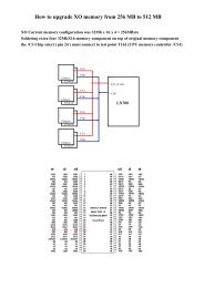
- Page 1 and 2: 4Gb, 8Gb, and 16Gb x8 NAND Flash Me
- Page 4: 4Gb, 8Gb, and 16Gb x8 NAND Flash Me
- Page 7 and 8: List of Tables4Gb, 8Gb, and 16Gb x8
- Page 9 and 10: 4Gb, 8Gb, and 16Gb x8 NAND Flash Me
- Page 11: 4Gb, 8Gb, and 16Gb x8 NAND Flash Me
- Page 15 and 16: 4Gb, 8Gb, and 16Gb x8 NAND Flash Me
- Page 17 and 18: 4Gb, 8Gb, and 16Gb x8 NAND Flash Me
- Page 19 and 20: 4Gb, 8Gb, and 16Gb x8 NAND Flash Me
- Page 21 and 22: 4Gb, 8Gb, and 16Gb x8 NAND Flash Me
- Page 23 and 24: 4Gb, 8Gb, and 16Gb x8 NAND Flash Me
- Page 25 and 26: 4Gb, 8Gb, and 16Gb x8 NAND Flash Me
- Page 27 and 28: 4Gb, 8Gb, and 16Gb x8 NAND Flash Me
- Page 29 and 30: 4Gb, 8Gb, and 16Gb x8 NAND Flash Me
- Page 31 and 32: 4Gb, 8Gb, and 16Gb x8 NAND Flash Me
- Page 33 and 34: 4Gb, 8Gb, and 16Gb x8 NAND Flash Me
- Page 35 and 36: 4Gb, 8Gb, and 16Gb x8 NAND Flash Me
- Page 37 and 38: 4Gb, 8Gb, and 16Gb x8 NAND Flash Me
- Page 39 and 40: 4Gb, 8Gb, and 16Gb x8 NAND Flash Me
- Page 41 and 42: 4Gb, 8Gb, and 16Gb x8 NAND Flash Me
- Page 43 and 44: 4Gb, 8Gb, and 16Gb x8 NAND Flash Me
- Page 45 and 46: 4Gb, 8Gb, and 16Gb x8 NAND Flash Me
- Page 47 and 48: Interleaved Die Operations4Gb, 8Gb,
- Page 49 and 50: 4Gb, 8Gb, and 16Gb x8 NAND Flash Me
- Page 51 and 52: 4Gb, 8Gb, and 16Gb x8 NAND Flash Me
- Page 53 and 54: 4Gb, 8Gb, and 16Gb x8 NAND Flash Me
- Page 55 and 56: PDF: 09005aef81b80e13/Source: 09005
- Page 57 and 58: WRITE PROTECT Operation4Gb, 8Gb, an
- Page 59 and 60: Electrical Characteristics4Gb, 8Gb,
- Page 61 and 62: 4Gb, 8Gb, and 16Gb x8 NAND Flash Me
- Page 63 and 64:
4Gb, 8Gb, and 16Gb x8 NAND Flash Me
- Page 65 and 66:
4Gb, 8Gb, and 16Gb x8 NAND Flash Me
- Page 67 and 68:
4Gb, 8Gb, and 16Gb x8 NAND Flash Me
- Page 69 and 70:
4Gb, 8Gb, and 16Gb x8 NAND Flash Me
- Page 71 and 72:
4Gb, 8Gb, and 16Gb x8 NAND Flash Me
- Page 73 and 74:
4Gb, 8Gb, and 16Gb x8 NAND Flash Me
- Page 75 and 76:
4Gb, 8Gb, and 16Gb x8 NAND Flash Me
- Page 77 and 78:
4Gb, 8Gb, and 16Gb x8 NAND Flash Me
- Page 79 and 80:
4Gb, 8Gb, and 16Gb x8 NAND Flash Me
- Page 81:
4Gb, 8Gb, and 16Gb x8 NAND Flash Me