

PIC16F84A 18-pin Enhanced Flash/EEPROM 8-Bit MCU Data Sheet
PIC16F84A 18-pin Enhanced Flash/EEPROM 8-Bit MCU Data Sheet
PIC16F84A 18-pin Enhanced Flash/EEPROM 8-Bit MCU Data Sheet

Create successful ePaper yourself
Turn your PDF publications into a flip-book with our unique Google optimized e-Paper software.
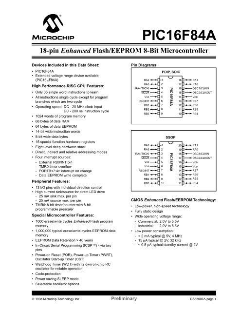
M<strong>PIC16F84A</strong><strong>18</strong>-<strong>pin</strong> <strong>Enhanced</strong> <strong>Flash</strong>/<strong>EEPROM</strong> 8-<strong>Bit</strong> MicrocontrollerDevices Included in this <strong>Data</strong> <strong>Sheet</strong>:• <strong>PIC16F84A</strong>• Extended voltage range device available(PIC16LF84A)High Performance RISC CPU Features:• Only 35 single word instructions to learn• All instructions single cycle except for programbranches which are two-cycle• Operating speed: DC - 20 MHz clock inputDC - 200 ns instruction cycle• 1024 words of program memory• 68 bytes of data RAM• 64 bytes of data <strong>EEPROM</strong>• 14-bit wide instruction words• 8-bit wide data bytes• 15 special function hardware registers• Eight-level deep hardware stack• Direct, indirect and relative addressing modes• Four interrupt sources:- External RB0/INT <strong>pin</strong>- TMR0 timer overflow- PORTB interrupt on change- <strong>Data</strong> <strong>EEPROM</strong> write completePeripheral Features:• 13 I/O <strong>pin</strong>s with individual direction control• High current sink/source for direct LED drive- 25 mA sink max. per <strong>pin</strong>- 25 mA source max. per <strong>pin</strong>• TMR0: 8-bit timer/counter with 8-bitprogrammable prescalerSpecial Microcontroller Features:• 1000 erase/write cycles <strong>Enhanced</strong> <strong>Flash</strong> programmemory• 1,000,000 typical erase/write cycles <strong>EEPROM</strong> datamemory• <strong>EEPROM</strong> <strong>Data</strong> Retention > 40 years• In-Circuit Serial Programming (ICSP) - via two<strong>pin</strong>s• Power-on Reset (POR), Power-up Timer (PWRT),Oscillator Start-up Timer (OST)• Watchdog Timer (WDT) with its own on-chip RCoscillator for reliable operation• Code-protection• Power saving SLEEP mode• Selectable oscillator optionsPin DiagramsRA2RA3RA4/T0CKIMCLRVSSRB0/INTRB1RB2RB3RA2RA3RA4/T0CKIMCLRVSSVSSRB0/INTRB1RB2RB3•123456789PDIP, SOIC<strong>PIC16F84A</strong>SSOP<strong>18</strong>1716151413121110•1202193<strong>18</strong>41751661571481391210 11<strong>PIC16F84A</strong>CMOS <strong>Enhanced</strong> <strong>Flash</strong>/EERPOM Technology:• Low-power, high-speed technology• Fully static design• Wide operating voltage range:- Commercial: 2.0V to 5.5V- Industrial: 2.0V to 5.5V• Low power consumption:- < 2 mA typical @ 5V, 4 MHz- 15 µA typical @ 2V, 32 kHz- < 0.5 µA typical standby current @ 2VRA1RA0OSC1/CLKINOSC2/CLKOUTVDDRB7RB6RB5RB4RA1RA0OSC1/CLKINOSC2/CLKOUTVDDVDDRB7RB6RB5RB4© 1998 Microchip Technology Inc. Preliminary DS35007A-page 1
<strong>PIC16F84A</strong>Table of Contents1.0 Device Overview ............................................................................................................................................................................ 32.0 Memory Organization..................................................................................................................................................................... 53.0 I/O Ports....................................................................................................................................................................................... 134.0 Timer0 Module ............................................................................................................................................................................. 175.0 <strong>Data</strong> <strong>EEPROM</strong> Memory............................................................................................................................................................... 196.0 Special Features of the CPU ....................................................................................................................................................... 217.0 Instruction Set Summary.............................................................................................................................................................. 338.0 Development Support .................................................................................................................................................................. 359.0 Electrical Characteristics for <strong>PIC16F84A</strong>..................................................................................................................................... 4110.0 DC & AC Characteristics Graphs/Tables ..................................................................................................................................... 5311.0 Packaging Information ................................................................................................................................................................. 55Appendix A: Revision History........................................................................................................................................................... 59Appendix B: Conversion Considerations.......................................................................................................................................... 59Appendix C: Migration from Baseline to Midrange Devices ............................................................................................................. 62Index ................................................................................................................................................................................................... 63On-Line Support................................................................................................................................................................................... 65Reader Response ................................................................................................................................................................................ 66<strong>PIC16F84A</strong> Product Identification System........................................................................................................................................... 67Most Current <strong>Data</strong> <strong>Sheet</strong>To Our Valued CustomersTo obtain the most up-to-date version of this data sheet, please check our Worldwide Web site at:http://www.microchip.comYou can determine the version of a data sheet by examining its literature number found on the bottom outside corner of any page.The last character of the literature number is the version number. e.g., DS30000A is version A of document DS30000.ErrataAn errata sheet may exist for current devices, describing minor operational differences (from the data sheet) and recommendedworkarounds. As device/documentation issues become known to us, we will publish an errata sheet. The errata will specify therevision of silicon and revision of document to which it applies.To determine if an errata sheet exists for a particular device, please check with one of the following:• Microchip’s Worldwide Web site; http://www.microchip.com• Your local Microchip sales office (see last page)• The Microchip Corporate Literature Center; U.S. FAX: (602) 786-7277When contacting a sales office or the literature center, please specify which device, revision of silicon and data sheet (include literaturenumber) you are using.Corrections to this <strong>Data</strong> <strong>Sheet</strong>We constantly strive to improve the quality of all our products and documentation. We have spent a great deal of time to ensurethat this document is correct. However, we realize that we may have missed a few things. If you find any information that is missingor appears in error, please:• Fill out and mail in the reader response form in the back of this data sheet.• E-mail us at webmaster@microchip.com.We appreciate your assistance in making this a better document.DS35007A-page 2 Preliminary © 1998 Microchip Technology Inc.
<strong>PIC16F84A</strong>1.0 DEVICE OVERVIEWThis document contains device-specific information forthe operation of the <strong>PIC16F84A</strong> device. Additionalinformation may be found in the PICmicro Mid-RangeReference Manual, (DS33023), which may be downloadedfrom the Microchip website. The ReferenceManual should be considered a complementary documentto this data sheet, and is highly recommendedreading for a better understanding of the device architectureand operation of the peripheral modules.The <strong>PIC16F84A</strong> belongs to the mid-range family of thePICmicro microcontroller devices. A block diagram ofthe device is shown in Figure 1-1.The program memory contains 1K words, which translatesto 1024 instructions, since each 14-bit programmemory word is the same width as each device instruction.The data memory (RAM) contains 68 bytes. <strong>Data</strong><strong>EEPROM</strong> is 64 bytes.There are also 13 I/O <strong>pin</strong>s that are user-configured ona <strong>pin</strong>-to-<strong>pin</strong> basis. Some <strong>pin</strong>s are multiplexed with otherdevice functions. These functions include:• External interrupt• Change on PORTB interrupt• Timer0 clock inputTable 1-1 details the <strong>pin</strong>out of the device with descriptionsand details for each <strong>pin</strong>.FIGURE 1-1:<strong>PIC16F84A</strong> BLOCK DIAGRAM<strong>Flash</strong>ProgramMemory<strong>PIC16F84A</strong>1K x 1413Program Counter8 Level Stack(13-bit)<strong>Data</strong> BusRAMFile Registers<strong>PIC16F84A</strong>68 x 88<strong>EEPROM</strong> <strong>Data</strong> MemoryEEDATA<strong>EEPROM</strong><strong>Data</strong> Memory64 x 8ProgramBus14Instruction reg7Addr MuxRAM AddrEEADR5Direct Addr7IndirectAddrTMR0FSR reg8STATUS regRA4/T0CKIInstructionDecode &ControlPower-upTimerOscillatorStart-up TimerPower-onResetALUMUX8I/O PortsRA3:RA0TimingGenerationWatchdogTimerW regRB7:RB1RB0/INTOSC2/CLKOUTOSC1/CLKINMCLRVDD, VSS© 1998 Microchip Technology Inc. Preliminary DS35007A-page 3
<strong>PIC16F84A</strong>TABLE 1-1<strong>PIC16F84A</strong> PINOUT DESCRIPTIONPin NameDIPNo.SOICNo.SSOPNo.I/O/PTypeBufferTypeDescriptionOSC1/CLKIN 16 16 <strong>18</strong> I ST/CMOS (3) Oscillator crystal input/external clock source input.OSC2/CLKOUT 15 15 19 O — Oscillator crystal output. Connects to crystal or resonator incrystal oscillator mode. In RC mode, OSC2 <strong>pin</strong> outputsCLKOUT which has 1/4 the frequency of OSC1, anddenotes the instruction cycle rate.MCLR 4 4 4 I/P ST Master clear (reset) input/programming voltage input. This<strong>pin</strong> is an active low reset to the device.PORTA is a bi-directional I/O port.RA0 17 17 19 I/O TTLRA1 <strong>18</strong> <strong>18</strong> 20 I/O TTLRA2 1 1 1 I/O TTLRA3 2 2 2 I/O TTLRA4/T0CKI 3 3 3 I/O ST Can also be selected to be the clock input to the TMR0timer/counter. Output is open drain type.PORTB is a bi-directional I/O port. PORTB can be softwareprogrammed for internal weak pull-up on all inputs.RB0/INT 6 6 7 I/O TTL/ST (1) RB0/INT can also be selected as an external interrupt<strong>pin</strong>.RB1 7 7 8 I/O TTLRB2 8 8 9 I/O TTLRB3 9 9 10 I/O TTLRB4 10 10 11 I/O TTL Interrupt on change <strong>pin</strong>.RB5 11 11 12 I/O TTL Interrupt on change <strong>pin</strong>.RB6 12 12 13 I/O TTL/ST (2) Interrupt on change <strong>pin</strong>. Serial programming clock.RB7 13 13 14 I/O TTL/ST (2) Interrupt on change <strong>pin</strong>. Serial programming data.VSS 5 5 5,6 P — Ground reference for logic and I/O <strong>pin</strong>s.VDD 14 14 15,16 P — Positive supply for logic and I/O <strong>pin</strong>s.Legend: I= input O = output I/O = Input/Output P = power— = Not used TTL = TTL input ST = Schmitt Trigger inputNote 1: This buffer is a Schmitt Trigger input when configured as the external interrupt.2: This buffer is a Schmitt Trigger input when used in serial programming mode.3: This buffer is a Schmitt Trigger input when configured in RC oscillator mode and a CMOS input otherwise.DS35007A-page 4 Preliminary © 1998 Microchip Technology Inc.
<strong>PIC16F84A</strong>2.0 MEMORY ORGANIZATIONThere are two memory blocks in the <strong>PIC16F84A</strong>.These are the program memory and the data memory.Each block has its own bus, so that access to eachblock can occur during the same oscillator cycle.The data memory can further be broken down into thegeneral purpose RAM and the Special FunctionRegisters (SFRs). The operation of the SFRs thatcontrol the “core” are described here. The SFRs usedto control the peripheral modules are described in thesection discussing each individual peripheral module.The data memory area also contains the data<strong>EEPROM</strong> memory. This memory is not directly mappedinto the data memory, but is indirectly mapped. That is,an indirect address pointer specifies the address of thedata <strong>EEPROM</strong> memory to read/write. The 64 bytes ofdata <strong>EEPROM</strong> memory have the address range0h-3Fh. More details on the <strong>EEPROM</strong> memory can befound in Section 5.0.Additional information on device memory may be foundin the PICmicro Mid-Range Reference Manual,(DS33023).2.1 Program Memory OrganizationThe PIC16FXX has a 13-bit program counter capableof addressing an 8K x 14 program memory space.For the <strong>PIC16F84A</strong>, the first 1K x 14 (0000h-03FFh)are physically implemented (Figure 2-1). Accessing alocation above the physically implemented address willcause a wraparound. For example, for locations 20h,420h, 820h, C20h, 1020h, 1420h, <strong>18</strong>20h, and 1C20hwill be the same instruction.The reset vector is at 0000h and the interrupt vector isat 0004h.FIGURE 2-1:PROGRAM MEMORY MAPAND STACK - <strong>PIC16F84A</strong>PCCALL, RETURN13RETFIE, RETLWStack Level 1•User MemorySpaceStack Level 8Reset VectorPeripheral Interrupt Vector0000h0004h3FFh1FFFh© 1998 Microchip Technology Inc. Preliminary DS35007A-page 5
<strong>PIC16F84A</strong>2.2 <strong>Data</strong> Memory OrganizationThe data memory is partitioned into two areas. The firstis the Special Function Registers (SFR) area, while thesecond is the General Purpose Registers (GPR) area.The SFRs control the operation of the device.Portions of data memory are banked. This is for boththe SFR area and the GPR area. The GPR area isbanked to allow greater than 116 bytes of generalpurpose RAM. The banked areas of the SFR are for theregisters that control the peripheral functions. Bankingrequires the use of control bits for bank selection.These control bits are located in the STATUS Register.Figure 2-1 shows the data memory map organization.Instructions MOVWF and MOVF can move values fromthe W register to any location in the register file (“F”),and vice-versa.The entire data memory can be accessed eitherdirectly using the absolute address of each register fileor indirectly through the File Select Register (FSR)(Section 2.4). Indirect addressing uses the presentvalue of the RP0 bit for access into the banked areas ofdata memory.<strong>Data</strong> memory is partitioned into two banks whichcontain the general purpose registers and the specialfunction registers. Bank 0 is selected by clearing theRP0 bit (STATUS). Setting the RP0 bit selects Bank1. Each Bank extends up to 7Fh (128 bytes). The firsttwelve locations of each Bank are reserved for theSpecial Function Registers. The remainder are GeneralPurpose Registers implemented as static RAM.2.2.1 GENERAL PURPOSE REGISTER FILEEach General Purpose Register (GPR) is 8 bits wideand is accessed either directly or indirectly through theFSR (Section 2.4).The GPR addresses in bank 1 are mapped toaddresses in bank 0. As an example, addressing location0Ch or 8Ch will access the same GPR.FIGURE 2-1: REGISTER FILE MAP -<strong>PIC16F84A</strong>File AddressFile Address00h01h02hIndirect addr. (1)TMR0PCLIndirect addr. (1)OPTION_REGPCL80h81h82h03h04h05h06h07h08h09h0Ah0Bh0ChSTATUSFSRPORTAPORTBEEDATAEEADRPCLATHINTCON68GeneralPurposeRegisters(SRAM)STATUSFSRTRISATRISBEECON1EECON2 (1)PCLATHINTCONMapped(accesses)in Bank 083h84h85h86h87h88h89h8Ah8Bh8Ch4Fh50hCFhD0h7FhFFhBank 0 Bank 1Unimplemented data memory location; read as '0'.Note 1:Not a physical register.DS35007A-page 6 Preliminary © 1998 Microchip Technology Inc.
<strong>PIC16F84A</strong>2.2.2 SPECIAL FUNCTION REGISTERSThe Special Function Registers (Figure 2-1 andTable 2-1) are used by the CPU and Peripheralfunctions to control the device operation. Theseregisters are static RAM.TABLE 2-1REGISTER FILE SUMMARYThe special function registers can be classified into twosets, core and peripheral. Those associated with thecore functions are described in this section. Thoserelated to the operation of the peripheral features aredescribed in the section for that specific feature.Addr Name <strong>Bit</strong> 7 <strong>Bit</strong> 6 <strong>Bit</strong> 5 <strong>Bit</strong> 4 <strong>Bit</strong> 3 <strong>Bit</strong> 2 <strong>Bit</strong> 1 <strong>Bit</strong> 0Value onPower-onResetValue on allother resets(Note3)Bank 000h INDF Uses contents of FSR to address data memory (not a physical register) ---- ---- ---- ----01h TMR0 8-bit real-time clock/counter xxxx xxxx uuuu uuuu02h PCL Low order 8 bits of the Program Counter (PC) 0000 0000 0000 000003h STATUS (2) IRP RP1 RP0 TO PD Z DC C 0001 1xxx 000q quuu04h FSR Indirect data memory address pointer 0 xxxx xxxx uuuu uuuu05h PORTA(4) — — — RA4/T0CKI RA3 RA2 RA1 RA0 ---x xxxx ---u uuuu06h (5)PORTBRB7 RB6 RB5 RB4 RB3 RB2 RB1 RB0/INT xxxx xxxx uuuu uuuu07h Unimplemented location, read as '0' ---- ---- ---- ----08h EEDATA <strong>EEPROM</strong> data register xxxx xxxx uuuu uuuu09h EEADR <strong>EEPROM</strong> address register xxxx xxxx uuuu uuuu0Ah PCLATH — — — Write buffer for upper 5 bits of the PC (1) ---0 0000 ---0 00000Bh INTCON GIE EEIE T0IE INTE RBIE T0IF INTF RBIF 0000 000x 0000 000uBank <strong>18</strong>0h INDF Uses contents of FSR to address data memory (not a physical register) ---- ---- ---- ----81h OPTION_REG RBPU INTEDG T0CS T0SE PSA PS2 PS1 PS0 1111 1111 1111 111<strong>18</strong>2h PCL Low order 8 bits of Program Counter (PC) 0000 0000 0000 000083h STATUS (2) IRP RP1 RP0 TO PD Z DC C 0001 1xxx 000q quuu84h FSR Indirect data memory address pointer 0 xxxx xxxx uuuu uuuu85h TRISA — — — PORTA data direction register ---1 1111 ---1 111<strong>18</strong>6h TRISB PORTB data direction register 1111 1111 1111 111<strong>18</strong>7h Unimplemented location, read as '0' ---- ---- ---- ----88h EECON1 — — — EEIF WRERR WREN WR RD ---0 x000 ---0 q00089h EECON2 <strong>EEPROM</strong> control register 2 (not a physical register) ---- ---- ---- ----0Ah PCLATH — — — Write buffer for upper 5 bits of the PC (1) ---0 0000 ---0 00000Bh INTCON GIE EEIE T0IE INTE RBIE T0IF INTF RBIF 0000 000x 0000 000uLegend: x = unknown, u = unchanged. - = unimplemented read as '0', q = value depends on condition.Note 1: The upper byte of the program counter is not directly accessible. PCLATH is a slave register for PC. The contentsof PCLATH can be transferred to the upper byte of the program counter, but the contents of PC is never transferredto PCLATH.2: The TO and PD status bits in the STATUS register are not affected by a MCLR reset.3: Other (non power-up) resets include: external reset through MCLR and the Watchdog Timer Reset.4: On any device reset, these <strong>pin</strong>s are configured as inputs.5: This is the value that will be in the port output latch.© 1998 Microchip Technology Inc. Preliminary DS35007A-page 7
<strong>PIC16F84A</strong>2.2.2.1 STATUS REGISTERThe STATUS register contains the arithmetic status ofthe ALU, the RESET status and the bank select bit fordata memory.As with any register, the STATUS register can be thedestination for any instruction. If the STATUS register isthe destination for an instruction that affects the Z, DCor C bits, then the write to these three bits is disabled.These bits are set or cleared according to device logic.Furthermore, the TO and PD bits are not writable.Therefore, the result of an instruction with the STATUSregister as destination may be different than intended.For example, CLRF STATUS will clear the upper-threebits and set the Z bit. This leaves the STATUS registeras 000u u1uu (where u = unchanged).Only the BCF, BSF, SWAPF and MOVWF instructionsshould be used to alter the STATUS register (Table 7-2)because these instructions do not affect any status bit.Note 1: The IRP and RP1 bits (STATUS) arenot used by the <strong>PIC16F84A</strong> and should beprogrammed as cleared. Use of these bitsas general purpose R/W bits is NOTrecommended, since this may affectupward compatibility with future products.Note 2: The C and DC bits operate as a borrowand digit borrow out bit, respectively, insubtraction. See the SUBLW and SUBWFinstructions for examples.Note 3: When the STATUS register is thedestination for an instruction that affectsthe Z, DC or C bits, then the write to thesethree bits is disabled. The specified bit(s)will be updated according to device logicFIGURE 2-1: STATUS REGISTER (ADDRESS 03h, 83h)R/W-0 R/W-0 R/W-0 R-1 R-1 R/W-x R/W-x R/W-xIRP RP1 RP0 TO PD Z DC C R = Readable bitbit7bit0 W = Writable bitU = Unimplemented bit,read as ‘0’- n = Value at POR resetbit 7: IRP: Register Bank Select bit (used for indirect addressing)The IRP bit is not used by the <strong>PIC16F84A</strong>. IRP should be maintained clear.bit 6-5: RP1:RP0: Register Bank Select bits (used for direct addressing)00 = Bank 0 (00h - 7Fh)01 = Bank 1 (80h - FFh)Each bank is 128 bytes. Only bit RP0 is used by the <strong>PIC16F84A</strong>. RP1 should be maintained clear.bit 4:bit 3:bit 2:bit 1:bit 0:TO: Time-out bit1 = After power-up, CLRWDT instruction, or SLEEP instruction0 = A WDT time-out occurredPD: Power-down bit1 = After power-up or by the CLRWDT instruction0 = By execution of the SLEEP instructionZ: Zero bit1 = The result of an arithmetic or logic operation is zero0 = The result of an arithmetic or logic operation is not zeroDC: Digit carry/borrow bit (for ADDWF and ADDLW instructions) (For borrow the polarity is reversed)1 = A carry-out from the 4th low order bit of the result occurred0 = No carry-out from the 4th low order bit of the resultC: Carry/borrow bit (for ADDWF and ADDLW instructions)1 = A carry-out from the most significant bit of the result occurred0 = No carry-out from the most significant bit of the result occurredNote:For borrow the polarity is reversed. A subtraction is executed by adding the two’s complement ofthe second operand. For rotate (RRF, RLF) instructions, this bit is loaded with either the high or loworder bit of the source register.DS35007A-page 8 Preliminary © 1998 Microchip Technology Inc.
<strong>PIC16F84A</strong>2.2.2.2 OPTION_REG REGISTERThe OPTION_REG register is a readable and writableregister which contains various control bits to configurethe TMR0/WDT prescaler, the external INT interrupt,TMR0, and the weak pull-ups on PORTB.Note:When the prescaler is assigned tothe WDT (PSA = '1'), TMR0 has a 1:1prescaler assignment.FIGURE 2-1: OPTION_REG REGISTER (ADDRESS 81h)R/W-1 R/W-1 R/W-1 R/W-1 R/W-1 R/W-1 R/W-1 R/W-1RBPU INTEDG T0CS T0SE PSA PS2 PS1 PS0 R = Readable bitbit7bit0 W = Writable bitU = Unimplemented bit,read as ‘0’- n = Value at POR resetbit 7: RBPU: PORTB Pull-up Enable bit1 = PORTB pull-ups are disabled0 = PORTB pull-ups are enabled (by individual port latch values)bit 6: INTEDG: Interrupt Edge Select bit1 = Interrupt on rising edge of RB0/INT <strong>pin</strong>0 = Interrupt on falling edge of RB0/INT <strong>pin</strong>bit 5: T0CS: TMR0 Clock Source Select bit1 = Transition on RA4/T0CKI <strong>pin</strong>0 = Internal instruction cycle clock (CLKOUT)bit 4: T0SE: TMR0 Source Edge Select bit1 = Increment on high-to-low transition on RA4/T0CKI <strong>pin</strong>0 = Increment on low-to-high transition on RA4/T0CKI <strong>pin</strong>bit 3: PSA: Prescaler Assignment bit1 = Prescaler assigned to the WDT0 = Prescaler assigned to TMR0bit 2-0: PS2:PS0: Prescaler Rate Select bits<strong>Bit</strong> Value TMR0 Rate WDT Rate0000010100111001011101111 : 21 : 41 : 81 : 161 : 321 : 641 : 1281 : 2561 : 11 : 21 : 41 : 81 : 161 : 321 : 641 : 128© 1998 Microchip Technology Inc. Preliminary DS35007A-page 9
<strong>PIC16F84A</strong>2.2.2.3 INTCON REGISTERThe INTCON register is a readable and writableregister which contains the various enable bits for allinterrupt sources.Note:Interrupt flag bits get set when an interruptcondition occurs regardless of the state ofits corresponding enable bit or the globalenable bit, GIE (INTCON).FIGURE 2-1: INTCON REGISTER (ADDRESS 0Bh, 8Bh)R/W-0 R/W-0 R/W-0 R/W-0 R/W-0 R/W-0 R/W-0 R/W-xGIE EEIE T0IE INTE RBIE T0IF INTF RBIF R = Readable bitbit7bit0 W = Writable bitU = Unimplemented bit,read as ‘0’- n = Value at POR resetbit 7: GIE: Global Interrupt Enable bit1 = Enables all un-masked interrupts0 = Disables all interruptsNote: For the operation of the interrupt structure, please refer to Section •.bit 6: EEIE: EE Write Complete Interrupt Enable bit1 = Enables the EE write complete interrupt0 = Disables the EE write complete interruptbit 5: T0IE: TMR0 Overflow Interrupt Enable bit1 = Enables the TMR0 interrupt0 = Disables the TMR0 interruptbit 4: INTE: RB0/INT Interrupt Enable bit1 = Enables the RB0/INT interrupt0 = Disables the RB0/INT interruptbit 3: RBIE: RB Port Change Interrupt Enable bit1 = Enables the RB port change interrupt0 = Disables the RB port change interruptbit 2: T0IF: TMR0 Overflow Interrupt Flag bit1 = TMR0 has overflowed (must be cleared in software)0 = TMR0 did not overflowbit 1: INTF: RB0/INT Interrupt Flag bit1 = The RB0/INT interrupt occurred0 = The RB0/INT interrupt did not occurbit 0: RBIF: RB Port Change Interrupt Flag bit1 = When at least one of the RB7:RB4 <strong>pin</strong>s changed state (must be cleared in software)0 = None of the RB7:RB4 <strong>pin</strong>s have changed stateDS35007A-page 10 Preliminary © 1998 Microchip Technology Inc.
<strong>PIC16F84A</strong>2.3 PCL and PCLATHThe program counter (PC) specifies the address of theinstruction to fetch for execution. The PC is 13 bitswide. The low byte is called the PCL register. This registeris readable and writable. The high byte is calledthe PCH register. This register contains the PCbits and is not directly readable or writable. All updatesto the PCH register go through the PCLATH register.2.3.1 STACKThe stack allows a combination of up to 8 program callsand interrupts to occur. The stack contains the returnaddress from this branch in program execution.Midrange devices have an 8 level deep x 13-bit widehardware stack. The stack space is not part of eitherprogram or data space and the stack pointer is notreadable or writable. The PC is PUSHed onto the stackwhen a CALL instruction is executed or an interruptcauses a branch. The stack is POPed in the event of aRETURN, RETLW or a RETFIE instruction execution.PCLATH is not modified when the stack is PUSHed orPOPed.After the stack has been PUSHed eight times, the ninthpush overwrites the value that was stored from the firstpush. The tenth push overwrites the second push (andso on).2.4 Indirect Addressing; INDF and FSRRegistersThe INDF register is not a physical register. AddressingINDF actually addresses the register whoseaddress is contained in the FSR register (FSR is apointer). This is indirect addressing.EXAMPLE 2-1: INDIRECT ADDRESSING• Register file 05 contains the value 10h• Register file 06 contains the value 0Ah• Load the value 05 into the FSR register• A read of the INDF register will return the value of10h• Increment the value of the FSR register by one(FSR = 06)• A read of the INDF register now will return thevalue of 0Ah.Reading INDF itself indirectly (FSR = 0) will produce00h. Writing to the INDF register indirectly results in ano-operation (although STATUS bits may be affected).A simple program to clear RAM locations 20h-2Fhusing indirect addressing is shown in Example 2-2.EXAMPLE 2-2: HOW TO CLEAR RAMUSING INDIRECTADDRESSINGmovlw 0x20 ;initialize pointermovwf FSR ; to RAMNEXT clrf INDF ;clear INDF registerincf FSR ;inc pointerbtfss FSR,4 ;all done?goto NEXT ;NO, clear nextCONTINUE: ;YES, continueAn effective 9-bit address is obtained by concatenatingthe 8-bit FSR register and the IRP bit (STATUS), asshown in Figure 2-1. However, IRP is not used in the<strong>PIC16F84A</strong>.© 1998 Microchip Technology Inc. Preliminary DS35007A-page 11
<strong>PIC16F84A</strong>FIGURE 2-1:DIRECT/INDIRECT ADDRESSINGDirect AddressingIndirect AddressingRP1 RP0 6 from opcode 0 IRP 7 (FSR) 0(2) (2)bank selectlocation selectbank selectlocation select00h00 0<strong>18</strong>0h0Bh0ChAddresses<strong>Data</strong>Memory (1) map backto Bank 04Fh50h(3) (3)7FhBank 0 Bank 1FFhNote 1: For memory map detail see Figure 2-1.2: Maintain as clear for upward compatiblity with future products.3: Not implemented.DS35007A-page 12 Preliminary © 1998 Microchip Technology Inc.
<strong>PIC16F84A</strong>3.0 I/O PORTSSome <strong>pin</strong>s for these I/O ports are multiplexed with analternate function for the peripheral features on thedevice. In general, when a peripheral is enabled, that<strong>pin</strong> may not be used as a general purpose I/O <strong>pin</strong>.Additional information on I/O ports may be found in thePICmicro Mid-Range Reference Manual,(DS33023).3.1 PORTA and TRISA RegistersPORTA is a 5-bit wide bi-directional port. The correspondingdata direction register is TRISA. Setting aTRISA bit (=1) will make the corresponding PORTA <strong>pin</strong>an input, i.e., put the corresponding output driver in ahi-impedance mode. Clearing a TRISA bit (=0) willmake the corresponding PORTA <strong>pin</strong> an output, i.e., putthe contents of the output latch on the selected <strong>pin</strong>.Note:On a Power-on Reset, these <strong>pin</strong>s are configuredas inputs and read as '0'.Reading the PORTA register reads the status of the<strong>pin</strong>s whereas writing to it will write to the port latch. Allwrite operations are read-modify-write operations.Therefore a write to a port implies that the port <strong>pin</strong>s areread, this value is modified, and then written to the portdata latch.Pin RA4 is multiplexed with the Timer0 module clockinput to become the RA4/T0CKI <strong>pin</strong>. The RA4/T0CKI<strong>pin</strong> is a Schmitt Trigger input and an open drain output.All other RA port <strong>pin</strong>s have TTL input levels and fullCMOS output drivers.FIGURE 3-1:<strong>Data</strong>busWRPortWRTRISRD PORTDDCKCKBLOCK DIAGRAM OF PINSRA3:RA0QQ<strong>Data</strong> LatchQQTRIS LatchRD TRISNote: I/O <strong>pin</strong>s have protection diodes to VDD and VSS.QENDVDDPNVSSTTLinputbufferI/O <strong>pin</strong>EXAMPLE 3-1: INITIALIZING PORTABCF STATUS, RP0 ;CLRF PORTA ; Initialize PORTA by; clearing output; data latchesBSF STATUS, RP0 ; Select Bank 1MOVLW 0x0F; Value used to; initialize data; directionMOVWF TRISA ; Set RA as inputs; RA4 as output; TRISA are always; read as '0'.© 1998 Microchip Technology Inc. Preliminary DS35007A-page 13
<strong>PIC16F84A</strong>FIGURE 3-2:BLOCK DIAGRAM OF PIN RA4<strong>Data</strong>busWRPORTD QCK Q<strong>Data</strong> LatchNRA4 <strong>pin</strong>WRTRISD QCK QTRIS LatchVSSSchmittTriggerinputbufferRD TRISQDRD PORTENTMR0 clock inputNote: I/O <strong>pin</strong> has protection diodes to VSS only.TABLE 3-1 PORTA FUNCTIONSName <strong>Bit</strong>0 Buffer Type FunctionRA0 bit0 TTL Input/outputRA1 bit1 TTL Input/outputRA2 bit2 TTL Input/outputRA3 bit3 TTL Input/outputRA4/T0CKI bit4 ST Input/output or external clock input for TMR0.Output is open drain type.Legend: TTL = TTL input, ST = Schmitt Trigger inputTABLE 3-2SUMMARY OF REGISTERS ASSOCIATED WITH PORTAAddress Name <strong>Bit</strong> 7 <strong>Bit</strong> 6 <strong>Bit</strong> 5 <strong>Bit</strong> 4 <strong>Bit</strong> 3 <strong>Bit</strong> 2 <strong>Bit</strong> 1 <strong>Bit</strong> 0Value onPower-onResetValue on allother resets05h PORTA — — — RA4/T0CKI RA3 RA2 RA1 RA0 ---x xxxx ---u uuuu85h TRISA — — — TRISA4 TRISA3 TRISA2 TRISA1 TRISA0 ---1 1111 ---1 1111Legend:x = unknown, u = unchanged, - = unimplemented read as '0'. Shaded cells are unimplemented, read as '0'DS35007A-page 14 Preliminary © 1998 Microchip Technology Inc.
<strong>PIC16F84A</strong>3.2 PORTB and TRISB RegistersPORTB is an 8-bit wide bi-directional port. The correspondingdata direction register is TRISB. Setting aTRISB bit (=1) will make the corresponding PORTB <strong>pin</strong>an input, i.e., put the corresponding output driver in ahi-impedance mode. Clearing a TRISB bit (=0) willmake the corresponding PORTB <strong>pin</strong> an output, i.e., putthe contents of the output latch on the selected <strong>pin</strong>.EXAMPLE 3-1: INITIALIZING PORTBBCF STATUS, RP0 ;CLRF PORTB ; Initialize PORTB by; clearing output; data latchesBSF STATUS, RP0 ; Select Bank 1MOVLW 0xCF; Value used to; initialize data; directionMOVWF TRISB ; Set RB as inputs; RB as outputs; RB as inputsEach of the PORTB <strong>pin</strong>s has a weak internal pull-up. Asingle control bit can turn on all the pull-ups. This is performedby clearing bit RBPU (OPTION). The weakpull-up is automatically turned off when the port <strong>pin</strong> isconfigured as an output. The pull-ups are disabled on aPower-on Reset.FIGURE 3-3:RBPU (1)<strong>Data</strong> busWR PortBLOCK DIAGRAM OF PINSRB7:RB4<strong>Data</strong> LatchDCKQFour of PORTB’s <strong>pin</strong>s, RB7:RB4, have an interrupt onchange feature. Only <strong>pin</strong>s configured as inputs cancause this interrupt to occur (i.e. any RB7:RB4 <strong>pin</strong> configuredas an output is excluded from the interrupt onchange comparison). The input <strong>pin</strong>s (of RB7:RB4) arecompared with the old value latched on the last read ofPORTB. The “mismatch” outputs of RB7:RB4 areOR’ed together to generate the RB Port Change Interruptwith flag bit RBIF (INTCON).This interrupt can wake the device from SLEEP. Theuser, in the interrupt service routine, can clear the interruptin the following manner:a) Any read or write of PORTB. This will end themismatch condition.b) Clear flag bit RBIF.A mismatch condition will continue to set flag bit RBIF.Reading PORTB will end the mismatch condition, andallow flag bit RBIF to be cleared.The interrupt on change feature is recommended forwake-up on key depression operation and operationswhere PORTB is only used for the interrupt on changefeature. Polling of PORTB is not recommended whileusing the interrupt on change feature.FIGURE 3-4:BLOCK DIAGRAM OF PINSRB3:RB0RBPU (1) weakPpull-up<strong>Data</strong> Latch<strong>Data</strong> busD QVDDI/OWR Port<strong>pin</strong> (2)weakCKPpull-upTRIS LatchD QTTLI/O<strong>pin</strong> (2) WR TRISInputCKBufferVDDWR TRISTRIS LatchD QCKTTLInputBufferRD TRISRD PortQDENSet RBIFRD TRISRD PortFrom otherRB7:RB4 <strong>pin</strong>sLatchQ DENQ DRB0/INTNoteSchmitt TriggerBuffer1: TRISB = '1' enables weak pull-up(if RBPU = '0' in the OPTION_REG register).2: I/O <strong>pin</strong>s have diode protection to VDD and VSS.RD PortENRD PortNote1: TRISB = '1' enables weak pull-up(if RBPU = '0' in the OPTION_REG register).2: I/O <strong>pin</strong>s have diode protection to VDD and VSS.© 1998 Microchip Technology Inc. Preliminary DS35007A-page 15
<strong>PIC16F84A</strong>TABLE 3-3PORTB FUNCTIONSName <strong>Bit</strong> Buffer Type I/O Consistency FunctionRB0/INT bit0 TTL/ST (1) Input/output <strong>pin</strong> or external interrupt input. Internal softwareprogrammable weak pull-up.RB1 bit1 TTL Input/output <strong>pin</strong>. Internal software programmable weak pull-up.RB2 bit2 TTL Input/output <strong>pin</strong>. Internal software programmable weak pull-up.RB3 bit3 TTL Input/output <strong>pin</strong>. Internal software programmable weak pull-up.RB4 bit4 TTL Input/output <strong>pin</strong> (with interrupt on change). Internal software programmableweak pull-up.RB5 bit5 TTL Input/output <strong>pin</strong> (with interrupt on change). Internal software programmableweak pull-up.RB6 bit6 TTL/ST (2) Input/output <strong>pin</strong> (with interrupt on change). Internal software programmableweak pull-up. Serial programming clock.RB7 bit7 TTL/ST (2) Input/output <strong>pin</strong> (with interrupt on change). Internal software programmableweak pull-up. Serial programming data.Legend: TTL = TTL input, ST = Schmitt Trigger.Note 1: This buffer is a Schmitt Trigger input when configured as the external interrupt.2: This buffer is a Schmitt Trigger input when used in serial programming mode.TABLE 3-4SUMMARY OF REGISTERS ASSOCIATED WITH PORTBAddr Name <strong>Bit</strong> 7 <strong>Bit</strong> 6 <strong>Bit</strong> 5 <strong>Bit</strong> 4 <strong>Bit</strong> 3 <strong>Bit</strong> 2 <strong>Bit</strong> 1 <strong>Bit</strong> 0Value onPower-onResetValue on allother resets06h PORTB RB7 RB6 RB5 RB4 RB3 RB2 RB1 RB0/INT xxxx xxxx uuuu uuuu86h TRISB TRISB7 TRISB6 TRISB5 TRISB4 TRISB3 TRISB2 TRISB1 TRISB0 1111 1111 1111 111<strong>18</strong>1h OPTION_REG RBPU INTEDG T0CS T0SE PSA PS2 PS1 PS0 1111 1111 1111 1111Legend:x = unknown, u = unchanged. Shaded cells are not used by PORTB.DS35007A-page 16 Preliminary © 1998 Microchip Technology Inc.
<strong>PIC16F84A</strong>4.0 TIMER0 MODULEThe Timer0 module timer/counter has the following features:• 8-bit timer/counter• Readable and writable• Internal or external clock select• Edge select for external clock• 8-bit software programmable prescaler• Interrupt on overflow from FFh to 00hFigure 4-1 is a simplified block diagram of the Timer0module.Additional information on timer modules is available inthe PICmicro Mid-Range Reference Manual,(DS33023).4.1 Timer0 OperationTimer0 can operate as a timer or as a counter.Timer mode is selected by clearing bit T0CS(OPTION_REG). In timer mode, the Timer0 modulewill increment every instruction cycle (without prescaler).If the TMR0 register is written, the increment isinhibited for the following two instruction cycles. Theuser can work around this by writing an adjusted valueto the TMR0 register.Counter mode is selected by setting bit T0CS(OPTION_REG). In counter mode, Timer0 willincrement either on every rising or falling edge of <strong>pin</strong>RA4/T0CKI. The incrementing edge is determined bythe Timer0 Source Edge Select bit T0SE(OPTION_REG). Clearing bit T0SE selects the risingedge. Restrictions on the external clock input arediscussed below.When an external clock input is used for Timer0, it mustmeet certain requirements. The requirements ensurethe external clock can be synchronized with the internalphase clock (TOSC). Also, there is a delay in the actualincrementing of Timer0 after synchronization.Additional information on external clock requirementsis available in the PICmicro Mid-Range ReferenceManual, (DS33023).4.2 PrescalerAn 8-bit counter is available as a prescaler for theTimer0 module, or as a postscaler for the WatchdogTimer, respectively (Figure 4-2). For simplicity, thiscounter is being referred to as “prescaler” throughoutthis data sheet. Note that there is only one prescaleravailable which is mutually exclusively shared betweenthe Timer0 module and the Watchdog Timer. Thus, aprescaler assignment for the Timer0 module meansthat there is no prescaler for the Watchdog Timer, andvice-versa.The prescaler is not readable or writable.The PSA and PS2:PS0 bits (OPTION_REG)determine the prescaler assignment and prescale ratio.Clearing bit PSA will assign the prescaler to the Timer0module. When the prescaler is assigned to the Timer0module, prescale values of 1:2, 1:4, ..., 1:256 areselectable.Setting bit PSA will assign the prescaler to the WatchdogTimer (WDT). When the prescaler is assigned tothe WDT, prescale values of 1:1, 1:2, ..., 1:128 areselectable.When assigned to the Timer0 module, all instructionswriting to the TMR0 register (e.g. CLRF 1, MOVWF 1,BSF 1,x....etc.) will clear the prescaler. Whenassigned to WDT, a CLRWDT instruction will clear theprescaler along with the WDT.Note:Writing to TMR0 when the prescaler isassigned to Timer0 will clear the prescalercount, but will not change the prescalerassignment.FIGURE 4-1:TIMER0 BLOCK DIAGRAMRA4/T0CKI<strong>pin</strong>T0SEFOSC/401T0CSProgrammablePrescaler3PS2, PS1, PS0Note 1: T0CS, T0SE, PSA, PS2:PS0 (OPTION_REG).2: The prescaler is shared with Watchdog Timer (refer to Figure 4-2 for detailed block diagram).10PSAPSoutSync withInternalclocksPSout(2 cycle delay)<strong>Data</strong> busTMR08Set interruptflag bit T0IFon overflow© 1998 Microchip Technology Inc. Preliminary DS35007A-page 17
<strong>PIC16F84A</strong>4.2.1 SWITCHING PRESCALER ASSIGNMENTThe prescaler assignment is fully under software control,i.e., it can be changed “on the fly” during programexecution.Note:To avoid an unintended device RESET, aspecific instruction sequence (shown in thePICmicro Mid-Range Reference Manual,DS3023) must be executed whenchanging the prescaler assignment fromTimer0 to the WDT. This sequence must befollowed even if the WDT is disabled.4.3 Timer0 InterruptThe TMR0 interrupt is generated when the TMR0 registeroverflows from FFh to 00h. This overflow sets bitT0IF (INTCON). The interrupt can be masked byclearing bit T0IE (INTCON). <strong>Bit</strong> T0IF must becleared in software by the Timer0 module interrupt serviceroutine before re-enabling this interrupt. TheTMR0 interrupt cannot awaken the processor fromSLEEP since the timer is shut off during SLEEP.FIGURE 4-2:BLOCK DIAGRAM OF THE TIMER0/WDT PRESCALERCLKOUT (=Fosc/4)<strong>Data</strong> BusRA4/T0CKI<strong>pin</strong>0MU1X1 0MUXSYNC2Cycles8TMR0 regT0SET0CSPSASet flag bit T0IFon OverflowWatchdogTimer01MUX8-bit Prescaler8PSA8 - to - 1MUXPS2:PS0WDT Enable bit0 1M U XPSAWDTTime-outNote: T0CS, T0SE, PSA, PS2:PS0 are (OPTION_REG).TABLE 4-1REGISTERS ASSOCIATED WITH TIMER0Address Name <strong>Bit</strong> 7 <strong>Bit</strong> 6 <strong>Bit</strong> 5 <strong>Bit</strong> 4 <strong>Bit</strong> 3 <strong>Bit</strong> 2 <strong>Bit</strong> 1 <strong>Bit</strong> 0Value onPOR,BORValue on allother resets01h TMR0 Timer0 module’s register xxxx xxxx uuuu uuuu0Bh,8Bh INTCON GIE PEIE T0IE INTE RBIE T0IF INTF RBIF 0000 000x 0000 000u81h OPTION_REG RBPU INTEDG T0CS T0SE PSA PS2 PS1 PS0 1111 1111 1111 111<strong>18</strong>5h TRISA — — PORTA <strong>Data</strong> Direction Register --11 1111 --11 1111Legend: x = unknown, u = unchanged, - = unimplemented locations read as '0'. Shaded cells are not used by Timer0.DS35007A-page <strong>18</strong> Preliminary © 1998 Microchip Technology Inc.
<strong>PIC16F84A</strong>5.0 DATA <strong>EEPROM</strong> MEMORYThe <strong>EEPROM</strong> data memory is readable and writableduring normal operation (full VDD range). This memoryis not directly mapped in the register file space. Insteadit is indirectly addressed through the Special FunctionRegisters. There are four SFRs used to read and writethis memory. These registers are:• EECON1• EECON2 (Not a physically implemented register)• EEDATA• EEADREEDATA holds the 8-bit data for read/write, and EEADRholds the address of the <strong>EEPROM</strong> location beingaccessed. <strong>PIC16F84A</strong> devices have 64 bytes of data<strong>EEPROM</strong> with an address range from 0h to 3Fh.The <strong>EEPROM</strong> data memory allows byte read and write.A byte write automatically erases the location andwrites the new data (erase before write). The <strong>EEPROM</strong>data memory is rated for high erase/write cycles. Thewrite time is controlled by an on-chip timer. The writetimewill vary with voltage and temperature as well asfrom chip to chip. Please refer to AC specifications forexact limits.When the device is code protected, the CPU maycontinue to read and write the data <strong>EEPROM</strong> memory.The device programmer can no longer accessthis memory.Additional information on the <strong>Data</strong> <strong>EEPROM</strong> is availablein the PICmicro Mid-Range Reference Manual,(DS33023).FIGURE 5-1: EECON1 REGISTER (ADDRESS 88h)U U U R/W-0 R/W-x R/W-0 R/S-0 R/S-x— — — EEIF WRERR WREN WR RD R = Readable bitbit7bit0 W = Writable bitS = Settable bitU = Unimplemented bit,read as ‘0’- n = Value at POR resetbit 7:5bit 4bit 3bit 2bit 1bit 0Unimplemented: Read as '0'EEIF: <strong>EEPROM</strong> Write Operation Interrupt Flag bit1 = The write operation completed (must be cleared in software)0 = The write operation is not complete or has not been startedWRERR: <strong>EEPROM</strong> Error Flag bit1 = A write operation is prematurely terminated(any MCLR reset or any WDT reset during normal operation)0 = The write operation completedWREN: <strong>EEPROM</strong> Write Enable bit1 = Allows write cycles0 = Inhibits write to the data <strong>EEPROM</strong>WR: Write Control bit1 = initiates a write cycle. (The bit is cleared by hardware once write is complete. The WR bit can onlybe set (not cleared) in software.0 = Write cycle to the data <strong>EEPROM</strong> is completeRD: Read Control bit1 = Initiates an <strong>EEPROM</strong> read (read takes one cycle. RD is cleared in hardware. The RD bit can onlybe set (not cleared) in software).0 = Does not initiate an <strong>EEPROM</strong> read© 1998 Microchip Technology Inc. Preliminary DS35007A-page 19
<strong>PIC16F84A</strong>5.1 Reading the <strong>EEPROM</strong> <strong>Data</strong> MemoryTo read a data memory location, the user must write theaddress to the EEADR register and then set control bitRD (EECON1). The data is available, in the verynext cycle, in the EEDATA register; therefore it can beread in the next instruction. EEDATA will hold this valueuntil another read or until it is written to by the user(during a write operation).EXAMPLE 5-1:DATA <strong>EEPROM</strong> READBCF STATUS, RP0 ; Bank 0MOVLW CONFIG_ADDR ;MOVWF EEADR ; Address to readBSF STATUS, RP0 ; Bank 1BSF EECON1, RD ; EE ReadBCF STATUS, RP0 ; Bank 0MOVF EEDATA, W ; W = EEDATA5.2 Writing to the <strong>EEPROM</strong> <strong>Data</strong> MemoryTo write an <strong>EEPROM</strong> data location, the user must firstwrite the address to the EEADR register and the datato the EEDATA register. Then the user must follow aspecific sequence to initiate the write for each byte.EXAMPLE 5-1:RequiredSequenceDATA <strong>EEPROM</strong> WRITEBSF STATUS, RP0 ; Bank 1BCF INTCON, GIE ; Disable INTs.BSF EECON1, WREN ; Enable WriteMOVLW 55h ;MOVWF EECON2 ; Write 55hMOVLW AAh ;MOVWF EECON2 ; Write AAhBSF EECON1,WR ; Set WR bit; begin writeBSF INTCON, GIE ; Enable INTs.The write will not initiate if the above sequence is notexactly followed (write 55h to EECON2, write AAh toEECON2, then set WR bit) for each byte. We stronglyrecommend that interrupts be disabled during thiscode segment.Additionally, the WREN bit in EECON1 must be set toenable write. This mechanism prevents accidentalwrites to data <strong>EEPROM</strong> due to errant (unexpected)code execution (i.e., lost programs). The user shouldkeep the WREN bit clear at all times, except whenupdating <strong>EEPROM</strong>. The WREN bit is not clearedby hardwareAfter a write sequence has been initiated, clearing theWREN bit will not affect this write cycle. The WR bit willbe inhibited from being set unless the WREN bit is set.At the completion of the write cycle, the WR bit iscleared in hardware and the EE Write CompleteInterrupt Flag bit (EEIF) is set. The user can eitherenable this interrupt or poll this bit. EEIF must becleared by software.5.3 Write VerifyDepending on the application, good programming practicemay dictate that the value written to the <strong>Data</strong><strong>EEPROM</strong> should be verified (Example 5-1) to thedesired value to be written. This should be used inapplications where an <strong>EEPROM</strong> bit will be stressednear the specification limit. The Total Endurance diskwill help determine your comfort level.Generally the <strong>EEPROM</strong> write failure will be a bit whichwas written as a '0', but reads back as a '1' (due toleakage off the bit).EXAMPLE 5-1:WRITE VERIFYBCF STATUS, RP0 ; Bank 0: ; Any code can go here: ;MOVF EEDATA, W ; Must be in Bank 0BSF STATUS, RP0 ; Bank 1READBSFEECON1, RD ; YES, Read the; value writtenBCF STATUS, RP0 ; Bank 0;; Is the value written (in W reg) and; read (in EEDATA) the same?;SUBWF EEDATA, W ;BTFSS STATUS, Z ; Is difference 0?GOTO WRITE_ERR ; NO, Write error: ; YES, Good write: ; Continue programTABLE 5-1REGISTERS/BITS ASSOCIATED WITH DATA <strong>EEPROM</strong>Address Name <strong>Bit</strong> 7 <strong>Bit</strong> 6 <strong>Bit</strong> 5 <strong>Bit</strong> 4 <strong>Bit</strong> 3 <strong>Bit</strong> 2 <strong>Bit</strong> 1 <strong>Bit</strong> 0Value onPower-onResetValue on allother resets08h EEDATA <strong>EEPROM</strong> data register xxxx xxxx uuuu uuuu09h EEADR <strong>EEPROM</strong> address register xxxx xxxx uuuu uuuu88h EECON1 — — — EEIF WRERR WREN WR RD ---0 x000 ---0 q00089h EECON2 <strong>EEPROM</strong> control register 2 ---- ---- ---- ----Legend:x = unknown, u = unchanged, - = unimplemented read as '0', q = value depends upon condition. Shaded cells are notused by data <strong>EEPROM</strong>.DS35007A-page 20 Preliminary © 1998 Microchip Technology Inc.
<strong>PIC16F84A</strong>6.0 SPECIAL FEATURES OF THECPUWhat sets a microcontroller apart from otherprocessors are special circuits to deal with the needs ofreal time applications. The <strong>PIC16F84A</strong> has a host ofsuch features intended to maximize system reliability,minimize cost through elimination of externalcomponents, provide power saving operating modesand offer code protection. These features are:• OSC Selection• Reset- Power-on Reset (POR)- Power-up Timer (PWRT)- Oscillator Start-up Timer (OST)• Interrupts• Watchdog Timer (WDT)• SLEEP• Code protection• ID locations• In-circuit serial programmingThe <strong>PIC16F84A</strong> has a Watchdog Timer which can beshut off only through configuration bits. It runs off itsown RC oscillator for added reliability. There are twotimers that offer necessary delays on power-up. One isthe Oscillator Start-up Timer (OST), intended to keepthe chip in reset until the crystal oscillator is stable. Theother is the Power-up Timer (PWRT), which provides afixed delay of 72 ms (nominal) on power-up only. Thisdesign keeps the device in reset while the power supplystabilizes. With these two timers on-chip, mostapplications need no external reset circuitry.SLEEP mode offers a very low current power-downmode. The user can wake-up from SLEEP throughexternal reset, Watchdog Timer time-out or through aninterrupt. Several oscillator options are provided toallow the part to fit the application. The RC oscillatoroption saves system cost while the LP crystal optionsaves power. A set of configuration bits are used toselect the various options.Additional information on special features is available inthe PICmicro Mid-Range Reference Manual,(DS33023).6.1 Configuration <strong>Bit</strong>sThe configuration bits can be programmed (read as '0')or left unprogrammed (read as '1') to select variousdevice configurations. These bits are mapped inprogram memory location 2007h.Address 2007h is beyond the user program memoryspace and it belongs to the special test/configurationmemory space (2000h - 3FFFh). This space can onlybe accessed during programming.FIGURE 6-1:CONFIGURATION WORD - <strong>PIC16F84A</strong>R/P-u R/P-u R/P-u R/P-u R/P-u R/P-u R/P-u R/P-u R/P-u R/P-u R/P-u R/P-u R/P-u R/P-uCP CP CP CP CP CP CP CP CP CP PWRTE WDTE FOSC1 FOSC0bit13bit0R = Readable bitP = Programmable bit- n = Value at POR resetu = unchangedbit 13:4 CP: Code Protection bit1 = Code protection off0 = All memory is code protectedbit 3 PWRTE: Power-up Timer Enable bit1 = Power-up timer is disabled0 = Power-up timer is enabledbit 2 WDTE: Watchdog Timer Enable bit1 = WDT enabled0 = WDT disabledbit 1:0 FOSC1:FOSC0: Oscillator Selection bits11 = RC oscillator10 = HS oscillator01 = XT oscillator00 = LP oscillator© 1998 Microchip Technology Inc. Preliminary DS35007A-page 21
<strong>PIC16F84A</strong>6.2 Oscillator Configurations6.2.1 OSCILLATOR TYPESThe <strong>PIC16F84A</strong> can be operated in four differentoscillator modes. The user can program twoconfiguration bits (FOSC1 and FOSC0) to select one ofthese four modes:• LP Low Power Crystal• XT Crystal/Resonator• HS High Speed Crystal/Resonator• RC Resistor/Capacitor6.2.2 CRYSTAL OSCILLATOR / CERAMICRESONATORSIn XT, LP or HS modes a crystal or ceramic resonatoris connected to the OSC1/CLKIN and OSC2/CLKOUT<strong>pin</strong>s to establish oscillation (Figure 6-2).FIGURE 6-2:C1 (1)C2 (1)CRYSTAL/CERAMICRESONATOR OPERATION(HS, XT OR LP OSCCONFIGURATION)Note1: See Table 6-1 for recommended values ofC1 and C2.2: A series resistor (RS) may be required forAT strip cut crystals.3: RF varies with the crystal chosen.The <strong>PIC16F84A</strong> oscillator design requires the use of aparallel cut crystal. Use of a series cut crystal may givea frequency out of the crystal manufacturersspecifications. When in XT, LP or HS modes, the devicecan have an external clock source to drive theOSC1/CLKIN <strong>pin</strong> (Figure 6-3).FIGURE 6-3:Clock fromext. systemOSC1XTALOSC2RS (2)OpenRF (3)SLEEPTointernallogicPIC16FXXEXTERNAL CLOCK INPUTOPERATION (HS, XT OR LPOSC CONFIGURATION)OSC1OSC2PIC16FXXTABLE 6-1Ranges Tested:TABLE 6-2CAPACITOR SELECTIONFOR CERAMIC RESONATORSMode Freq OSC1/C1 OSC2/C2XT 455 kHz2.0 MHz4.0 MHz47 - 100 pF15 - 33 pF15 - 33 pF47 - 100 pF15 - 33 pF15 - 33 pFHS8.0 MHz10.0 MHz15 - 33 pF15 - 33 pF15 - 33 pF15 - 33 pFNote : Recommended values of C1 and C2 are identical tothe ranges tested table.Higher capacitance increases the stability of theoscillator but also increases the start-up time.These values are for design guidance only. Sinceeach resonator has its own characteristics, the usershould consult the resonator manufacturer for theappropriate values of external components.Resonators Tested:455 kHz Panasonic EFO-A455K04B ± 0.3%2.0 MHz Murata Erie CSA2.00MG ± 0.5%4.0 MHz Murata Erie CSA4.00MG ± 0.5%8.0 MHz Murata Erie CSA8.00MT ± 0.5%10.0 MHz Murata Erie CSA10.00MTZ ± 0.5%None of the resonators had built-in capacitors.CAPACITOR SELECTIONFOR CRYSTAL OSCILLATORMode Freq OSC1/C1 OSC2/C2LP 32 kHz 68 - 100 pF 68 - 100 pF200 kHz 15 - 33 pF 15 - 33 pFXTHSNote :100 kHz2 MHz4 MHz4 MHz10 MHz100 - 150 pF15 - 33 pF15 - 33 pF15 - 33 pF15 - 33 pF100 - 150 pF15 - 33 pF15 - 33 pF15 - 33 pF15 - 33 pFHigher capacitance increases the stability ofoscillator but also increases the start-up time.These values are for design guidance only. Rs maybe required in HS mode as well as XT mode toavoid overdriving crystals with low drive level specification.Since each crystal has its own characteristics,the user should consult the crystalmanufacturer for appropriate values of externalcomponents.For VDD > 4.5V, C1 = C2 ≈ 30 pF is recommended.Crystals Tested:32.768 kHz Epson C-001R32.768K-A ± 20 PPM100 kHz Epson C-2 100.00 KC-P ± 20 PPM200 kHz STD XTL 200.000 KHz ± 20 PPM1.0 MHz ECS ECS-10-13-2 ± 50 PPM2.0 MHz ECS ECS-20-S-2 ± 50 PPM4.0 MHz ECS ECS-40-S-4 ± 50 PPM10.0 MHz ECS ECS-100-S-4 ± 50 PPMDS35007A-page 22 Preliminary © 1998 Microchip Technology Inc.
<strong>PIC16F84A</strong>6.2.3 RC OSCILLATORFor timing insensitive applications the RC device optionoffers additional cost savings. The RC oscillatorfrequency is a function of the supply voltage, theresistor (Rext) values, capacitor (Cext) values, and theoperating temperature. In addition to this, the oscillatorfrequency will vary from unit to unit due to normalprocess parameter variation. Furthermore, thedifference in lead frame capacitance between packagetypes also affects the oscillation frequency, especiallyfor low Cext values. The user needs to take intoaccount variation due to tolerance of the externalR and C components. Figure 6-4 shows how an R/Ccombination is connected to the <strong>PIC16F84A</strong>.FIGURE 6-4:RextCextVDDRC OSCILLATOR MODEOSC1VSSOSC2/CLKOUTFosc/4Recommended values: 5 kΩ ≤ Rext ≤ 100 kΩCext > 20pFInternalclockPIC16FXX6.3 ResetThe <strong>PIC16F84A</strong> differentiates between various kindsof reset:• Power-on Reset (POR)• MCLR reset during normal operation• MCLR reset during SLEEP• WDT Reset (during normal operation)• WDT Wake-up (during SLEEP)Figure 6-5 shows a simplified block diagram of theon-chip reset circuit. The MCLR reset path has a noisefilter to ignore small pulses. The electrical specificationsstate the pulse width requirements for the MCLR<strong>pin</strong>.Some registers are not affected in any reset condition;their status is unknown on a POR reset and unchangedin any other reset. Most other registers are reset to a“reset state” on POR, MCLR or WDT reset duringnormal operation and on MCLR reset during SLEEP.They are not affected by a WDT reset during SLEEP,since this reset is viewed as the resumption of normaloperation.Table 6-3 gives a description of reset conditions for theprogram counter (PC) and the STATUS register.Table 6-4 gives a full description of reset states for allregisters.The TO and PD bits are set or cleared differently in differentreset situations (Section 6.7). These bits areused in software to determine the nature of the reset.FIGURE 6-5:SIMPLIFIED BLOCK DIAGRAM OF ON-CHIP RESET CIRCUITExternalResetMCLRWDTModuleSLEEPWDTTime_OutResetVDDVDD risedetectOST/PWRTOSTPower_on_Reset10-bit Ripple counterSRQChip_ResetOSC1/CLKINOn-chipRC OSC (1)PWRT10-bit Ripple counterEnable PWRTNote 1:This is a separate oscillator from theRC oscillator of the CLKIN <strong>pin</strong>.Enable OSTSee Table 6-5© 1998 Microchip Technology Inc. Preliminary DS35007A-page 23
<strong>PIC16F84A</strong>TABLE 6-3RESET CONDITION FOR PROGRAM COUNTER AND THE STATUS REGISTERCondition Program Counter STATUS RegisterPower-on Reset 000h 0001 1xxxMCLR Reset during normal operation 000h 000u uuuuMCLR Reset during SLEEP 000h 0001 0uuuWDT Reset (during normal operation) 000h 0000 1uuuWDT Wake-up PC + 1 uuu0 0uuuInterrupt wake-up from SLEEP PC + 1 (1) uuu1 0uuuLegend: u = unchanged, x = unknown.Note 1: When the wake-up is due to an interrupt and the GIE bit is set, the PC is loaded with the interrupt vector(0004h).TABLE 6-4RESET CONDITIONS FOR ALL REGISTERSRegister Address Power-on ResetMCLR Reset during:– normal operation– SLEEPWDT Reset during normaloperationWake-up from SLEEP:– through interrupt– through WDT Time-outW — xxxx xxxx uuuu uuuu uuuu uuuuINDF 00h ---- ---- ---- ---- ---- ----TMR0 01h xxxx xxxx uuuu uuuu uuuu uuuuPCL 02h 0000h 0000h PC + 1 (2)STATUS 03h 0001 1xxx 000q quuu (3) uuuq quuu (3)FSR 04h xxxx xxxx uuuu uuuu uuuu uuuuPORTA (4) 05h ---x xxxx ---u uuuu ---u uuuuPORTB (5) 06h xxxx xxxx uuuu uuuu uuuu uuuuEEDATA 08h xxxx xxxx uuuu uuuu uuuu uuuuEEADR 09h xxxx xxxx uuuu uuuu uuuu uuuuPCLATH 0Ah ---0 0000 ---0 0000 ---u uuuuINTCON 0Bh 0000 000x 0000 000u uuuu uuuu (1)INDF 80h ---- ---- ---- ---- ---- ----OPTION_REG 81h 1111 1111 1111 1111 uuuu uuuuPCL 82h 0000h 0000h PC + 1STATUS 83h 0001 1xxx 000q quuu (3) uuuq quuu (3)FSR 84h xxxx xxxx uuuu uuuu uuuu uuuuTRISA 85h ---1 1111 ---1 1111 ---u uuuuTRISB 86h 1111 1111 1111 1111 uuuu uuuuEECON1 88h ---0 x000 ---0 q000 ---0 uuuuEECON2 89h ---- ---- ---- ---- ---- ----PCLATH 8Ah ---0 0000 ---0 0000 ---u uuuuINTCON 8Bh 0000 000x 0000 000u uuuu uuuu (1)Legend: u = unchanged, x = unknown, - = unimplemented bit read as '0', q = value depends on condition.Note 1: One or more bits in INTCON will be affected (to cause wake-up).2: When the wake-up is due to an interrupt and the GIE bit is set, the PC is loaded with the interrupt vector (0004h).3: Table 6-3 lists the reset value for each specific condition.4: On any device reset, these <strong>pin</strong>s are configured as inputs.5: This is the value that will be in the port output latch.DS35007A-page 24 Preliminary © 1998 Microchip Technology Inc.
<strong>PIC16F84A</strong>6.4 Power-on Reset (POR)A Power-on Reset pulse is generated on-chip whenVDD rise is detected (in the range of 1.2V - 1.7V). Totake advantage of the POR, just tie the MCLR <strong>pin</strong>directly (or through a resistor) to VDD. This willeliminate external RC components usually needed tocreate Power-on Reset. A minimum rise time for VDDmust be met for this to operate properly. See ElectricalSpecifications for details.When the device starts normal operation (exits thereset condition), device operating parameters (voltage,frequency, temperature, ...) must be meet to ensureoperation. If these conditions are not met, the devicemust be held in reset until the operating conditionsare met.For additional information, refer to Application NoteAN607, "Power-up Trouble Shooting."The POR circuit does not produce an internal resetwhen VDD declines.6.5 Power-up Timer (PWRT)The Power-up Timer (PWRT) provides a fixed 72 msnominal time-out (TPWRT) from POR (Figure 6-7,Figure 6-8, Figure 6-9 and Figure 6-10). The Power-upTimer operates on an internal RC oscillator. The chip iskept in reset as long as the PWRT is active. The PWRTdelay allows the VDD to rise to an acceptable level (Possibleexception shown in Figure 6-10).A configuration bit, PWRTE, can enable/disable thePWRT. See Figure 6-1 for the operation of the PWRTEbit for a particular device.The power-up time delay TPWRT will vary from chip tochip due to VDD, temperature, and process variation.See DC parameters for details.FIGURE 6-6:VDDDEXTERNAL POWER-ONRESET CIRCUIT (FOR SLOWVDD POWER-UP)VDDRCR1MCLRPIC16FXXNote 1: External Power-on Reset circuit is requiredonly if VDD power-up rate is too slow. Thediode D helps discharge the capacitorquickly when VDD powers down.2: R < 40 kΩ is recommended to make surethat voltage drop across R does not exceed0.2V (max leakage current spec on MCLR<strong>pin</strong> is 5 µA). A larger voltage drop willdegrade VIH level on the MCLR <strong>pin</strong>.3: R1 = 100Ω to 1 kΩ will limit any currentflowing into MCLR from externalcapacitor C in the event of an MCLR <strong>pin</strong>breakdown due to ESD or EOS.6.6 Oscillator Start-up Timer (OST)The Oscillator Start-up Timer (OST) provides a 1024oscillator cycle delay (from OSC1 input) after thePWRT delay ends (Figure 6-7, Figure 6-8, Figure 6-9and Figure 6-10). This ensures the crystal oscillator orresonator has started and stabilized.The OST time-out (TOST) is invoked only for XT, LP andHS modes and only on Power-on Reset or wake-upfrom SLEEP.When VDD rises very slowly, it is possible that theTPWRT time-out and TOST time-out will expire beforeVDD has reached its final value. In this case(Figure 6-10), an external power-on reset circuit maybe necessary (Figure 6-6).© 1998 Microchip Technology Inc. Preliminary DS35007A-page 25
<strong>PIC16F84A</strong>FIGURE 6-7: TIME-OUT SEQUENCE ON POWER-UP (MCLR NOT TIED TO VDD): CASE 1VDDMCLRINTERNAL PORTPWRTPWRT TIME-OUTTOSTOST TIME-OUTINTERNAL RESETFIGURE 6-8: TIME-OUT SEQUENCE ON POWER-UP (MCLR NOT TIED TO VDD): CASE 2VDDMCLRINTERNAL PORTPWRTPWRT TIME-OUTTOSTOST TIME-OUTINTERNAL RESETDS35007A-page 26 Preliminary © 1998 Microchip Technology Inc.
<strong>PIC16F84A</strong>FIGURE 6-9:TIME-OUT SEQUENCE ON POWER-UP (MCLR TIED TO VDD): FAST VDD RISE TIMEVDDMCLRINTERNAL PORTPWRTPWRT TIME-OUTTOSTOST TIME-OUTINTERNAL RESETFIGURE 6-10:TIME-OUT SEQUENCE ON POWER-UP (MCLR TIED TO VDD): SLOW VDD RISE TIMEV1VDDMCLRINTERNAL PORTPWRTPWRT TIME-OUTTOSTOST TIME-OUTINTERNAL RESETWhen VDD rises very slowly, it is possible that the TPWRT time-out and TOST time-out will expire before VDDhas reached its final value. In this example, the chip will reset properly if, and only if, V1 ≥ VDD min.© 1998 Microchip Technology Inc. Preliminary DS35007A-page 27
<strong>PIC16F84A</strong>6.7 Time-out Sequence and Power-downStatus <strong>Bit</strong>s (TO/PD)On power-up (Figure 6-7, Figure 6-8, Figure 6-9 andFigure 6-10) the time-out sequence is as follows: FirstPWRT time-out is invoked after a POR has expired.Then the OST is activated. The total time-out will varybased on oscillator configuration and PWRTEconfiguration bit status. For example, in RC mode withthe PWRT disabled, there will be no time-out at all.TABLE 6-5OscillatorConfigurationTIME-OUT IN VARIOUSSITUATIONSSince the time-outs occur from the POR reset pulse, ifMCLR is kept low long enough, the time-outs willexpire. Then bringing MCLR high, execution will beginimmediately (Figure 6-7). This is useful for testingpurposes or to synchronize more than one <strong>PIC16F84A</strong>device when operating in parallel.Table 6-6 shows the significance of the TO and PD bits.Table 6-3 lists the reset conditions for some specialregisters, while Table 6-4 lists the reset conditions forall the registers.TABLE 6-6PWRTEnabledXT, HS, LP 72 ms +1024TOSCPower-upPWRTDisabled1024TOSCWake-upfromSLEEP1024TOSCRC 72 ms — —STATUS BITS AND THEIRSIGNIFICANCETO PD Condition1 1 Power-on Reset0 x Illegal, TO is set on PORx 0 Illegal, PD is set on POR0 1 WDT Reset (during normal operation)0 0 WDT Wake-up1 1 MCLR Reset during normal operation1 0 MCLR Reset during SLEEP or interruptwake-up from SLEEP6.8 InterruptsThe <strong>PIC16F84A</strong> has 4 sources of interrupt:• External interrupt RB0/INT <strong>pin</strong>• TMR0 overflow interrupt• PORTB change interrupts (<strong>pin</strong>s RB7:RB4)• <strong>Data</strong> <strong>EEPROM</strong> write complete interruptThe interrupt control register (INTCON) recordsindividual interrupt requests in flag bits. It also containsthe individual and global interrupt enable bits.The global interrupt enable bit, GIE (INTCON)enables (if set) all un-masked interrupts or disables (ifcleared) all interrupts. Individual interrupts can bedisabled through their corresponding enable bits inINTCON register. <strong>Bit</strong> GIE is cleared on reset.The “return from interrupt” instruction, RETFIE, exitsinterrupt routine as well as sets the GIE bit, whichre-enable interrupts.The RB0/INT <strong>pin</strong> interrupt, the RB port change interruptand the TMR0 overflow interrupt flags are containedin the INTCON register.When an interrupt is responded to; the GIE bit iscleared to disable any further interrupt, the returnaddress is pushed onto the stack and the PC is loadedwith 0004h. For external interrupt events, such as theRB0/INT <strong>pin</strong> or PORTB change interrupt, the interruptlatency will be three to four instruction cycles. Theexact latency depends when the interrupt event occurs.The latency is the same for both one and two cycleinstructions. Once in the interrupt service routine thesource(s) of the interrupt can be determined by pollingthe interrupt flag bits. The interrupt flag bit(s) must becleared in software before re-enabling interrupts toavoid infinite interrupt requests.Note 1: Individual interrupt flag bits are setregardless of the status of theircorresponding mask bit or the GIE bit.FIGURE 6-11:T0IFT0IEINTFINTERBIFRBIEEEIFEEIEINTERRUPT LOGICWake-up(If in SLEEP mode)Interrupt to CPUGIEDS35007A-page 28 Preliminary © 1998 Microchip Technology Inc.
<strong>PIC16F84A</strong>6.8.1 INT INTERRUPTExternal interrupt on RB0/INT <strong>pin</strong> is edge triggered:either rising if INTEDG bit (OPTION_REG) is set,or falling, if INTEDG bit is clear. When a valid edgeappears on the RB0/INT <strong>pin</strong>, the INTF bit(INTCON) is set. This interrupt can be disabled byclearing control bit INTE (INTCON). Flag bit INTFmust be cleared in software via the interrupt serviceroutine before re-enabling this interrupt. The INTinterrupt can wake the processor from SLEEP(Section 6.11) only if the INTE bit was set prior to goinginto SLEEP. The status of the GIE bit decides whetherthe processor branches to the interrupt vectorfollowing wake-up.6.8.2 TMR0 INTERRUPTAn overflow (FFh → 00h) in TMR0 will set flag bit T0IF(INTCON). The interrupt can be enabled/disabledby setting/clearing enable bit T0IE (INTCON)(Section 4.0).6.8.3 PORB INTERRUPTAn input change on PORTB sets flag bit RBIF(INTCON). The interrupt can be enabled/disabledby setting/clearing enable bit RBIE (INTCON)(Section 3.2).Note 1: For a change on the I/O <strong>pin</strong> to berecognized, the pulse width must be atleast TCY wide.6.8.4 DATA <strong>EEPROM</strong> INTERRUPTAt the completion of a data <strong>EEPROM</strong> write cycle, flagbit EEIF (EECON1) will be set. The interrupt can beenabled/disabled by setting/clearing enable bit EEIE(INTCON) (Section 5.0).6.9 Context Saving During InterruptsDuring an interrupt, only the return PC value is savedon the stack. Typically, users wish to save key registervalues during an interrupt (e.g., W register and STATUSregister). This is implemented in software.Example 6-1 stores and restores the STATUS and Wregister’s values. The User defined registers, W_TEMPand STATUS_TEMP are the temporary storagelocations for the W and STATUS registers values.Example 6-1 does the following:a) Stores the W register.b) Stores the STATUS register in STATUS_TEMP.c) Executes the Interrupt Service Routine code.d) Restores the STATUS (and bank select bit)register.e) Restores the W register.EXAMPLE 6-1: SAVING STATUS AND W REGISTERS IN RAMPUSH MOVWF W_TEMP ; Copy W to TEMP register,SWAPF STATUS, W ; Swap status to be saved into WMOVWF STATUS_TEMP ; Save status to STATUS_TEMP registerISR : :: ; Interrupt Service Routine: ; should configure Bank as required: ;POP SWAPF STATUS_TEMP, W ; Swap nibbles in STATUS_TEMP register; and place result into WMOVWF STATUS ; Move W into STATUS register; (sets bank to original state)SWAPF W_TEMP, F ; Swap nibbles in W_TEMP and place result in W_TEMPSWAPF W_TEMP, W ; Swap nibbles in W_TEMP and place result into W© 1998 Microchip Technology Inc. Preliminary DS35007A-page 29
<strong>PIC16F84A</strong>6.10 Watchdog Timer (WDT)The Watchdog Timer is a free running on-chip RCoscillator which does not require any externalcomponents. This RC oscillator is separate from theRC oscillator of the OSC1/CLKIN <strong>pin</strong>. That means thatthe WDT will run even if the clock on the OSC1/CLKINand OSC2/CLKOUT <strong>pin</strong>s of the device has beenstopped, for example, by execution of a SLEEPinstruction. During normal operation a WDT time-outgenerates a device RESET. If the device is in SLEEPmode, a WDT Wake-up causes the device to wake-upand continue with normal operation. The WDT can bepermanently disabled by programming configuration bitWDTE as a '0' (Section 6.1).6.10.1 WDT PERIODThe WDT has a nominal time-out period of <strong>18</strong> ms, (withno prescaler). The time-out periods vary withtemperature, VDD and process variations from part topart (see DC specs). If longer time-out periods aredesired, a prescaler with a division ratio of up to 1:128can be assigned to the WDT under software control bywriting to the OPTION_REG register. Thus, time-outperiods up to 2.3 seconds can be realized.The CLRWDT and SLEEP instructions clear the WDTand the postscaler (if assigned to the WDT) and preventit from timing out and generating a deviceRESET condition.The TO bit in the STATUS register will be cleared upona WDT time-out.6.10.2 WDT PROGRAMMING CONSIDERATIONSIt should also be taken into account that under worstcase conditions (VDD = Min., Temperature = Max., max.WDT prescaler) it may take several seconds before aWDT time-out occurs.FIGURE 6-12:WATCHDOG TIMER BLOCK DIAGRAMFrom TMR0 Clock Source(Figure 4-2)WDT Timer01•MUXPostscaler88 - to -1 MUXPS2:PS0WDTEnable <strong>Bit</strong>PSA•To TMR0 (Figure 4-2)01MUXPSAWDTTime-outNote: PSA and PS2:PS0 are bits in the OPTION_REG register.TABLE 6-7SUMMARY OF REGISTERS ASSOCIATED WITH THE WATCHDOG TIMERAddr Name <strong>Bit</strong> 7 <strong>Bit</strong> 6 <strong>Bit</strong> 5 <strong>Bit</strong> 4 <strong>Bit</strong> 3 <strong>Bit</strong> 2 <strong>Bit</strong> 1 <strong>Bit</strong> 0Value onPower-onResetValue on allother resets2007h Config. bits (2) (2) (2) (2) PWRTE (1) WDTE FOSC1 FOSC0 (2)81h OPTION_REG RBPU INTEDG T0CS T0SE PSA PS2 PS1 PS0 1111 1111 1111 1111Legend: x = unknown. Shaded cells are not used by the WDT.Note 1: See Figure 6-1 for operation of the PWRTE bit.2: See Figure 6-1 and Section 6.12 for operation of the Code and <strong>Data</strong> protection bits.DS35007A-page 30 Preliminary © 1998 Microchip Technology Inc.
<strong>PIC16F84A</strong>6.11 Power-down Mode (SLEEP)A device may be powered down (SLEEP) and laterpowered up (Wake-up from SLEEP).6.11.1 SLEEPThe Power-down mode is entered by executing theSLEEP instruction.If enabled, the Watchdog Timer is cleared (but keepsrunning), the PD bit (STATUS) is cleared, the TO bit(STATUS) is set, and the oscillator driver is turnedoff. The I/O ports maintain the status they had beforethe SLEEP instruction was executed (driving high, low,or hi-impedance).For the lowest current consumption in SLEEP mode,place all I/O <strong>pin</strong>s at either at VDD or VSS, with noexternal circuitry drawing current from the I/O <strong>pin</strong>s, anddisable external clocks. I/O <strong>pin</strong>s that are hi-impedanceinputs should be pulled high or low externally to avoidswitching currents caused by floating inputs. TheT0CKI input should also be at VDD or VSS. Thecontribution from on-chip pull-ups on PORTB should beconsidered.The MCLR <strong>pin</strong> must be at a logic high level (VIHMC).It should be noted that a RESET generated by a WDTtime-out does not drive the MCLR <strong>pin</strong> low.6.11.2 WAKE-UP FROM SLEEPThe device can wake-up from SLEEP through one ofthe following events:1. External reset input on MCLR <strong>pin</strong>.2. WDT Wake-up (if WDT was enabled).3. Interrupt from RB0/INT <strong>pin</strong>, RB port change, ordata <strong>EEPROM</strong> write complete.Peripherals cannot generate interrupts during SLEEP,since no on-chip Q clocks are present.The first event (MCLR reset) will cause a device reset.The two latter events are considered a continuation ofprogram execution. The TO and PD bits can be used todetermine the cause of a device reset. The PD bit,which is set on power-up, is cleared when SLEEP isinvoked. The TO bit is cleared if a WDT time-outoccurred (and caused wake-up).While the SLEEP instruction is being executed, the nextinstruction (PC + 1) is pre-fetched. For the device towake-up through an interrupt event, the correspondinginterrupt enable bit must be set (enabled). Wake-upoccurs regardless of the state of the GIE bit. If the GIEbit is clear (disabled), the device continues execution atthe instruction after the SLEEP instruction. If the GIE bitis set (enabled), the device executes the instructionafter the SLEEP instruction and then branches to theinterrupt address (0004h). In cases where theexecution of the instruction following SLEEP is notdesirable, the user should have a NOP after theSLEEP instruction.FIGURE 6-13:WAKE-UP FROM SLEEP THROUGH INTERRUPTOSC1CLKOUT(4)Q1 Q2 Q3 Q4 Q1 Q2 Q3 Q4 Q1 Q1 Q2 Q3 Q4 Q1 Q2 Q3 Q4 Q1 Q2 Q3 Q4 Q1 Q2 Q3 Q4TOST(2)INT <strong>pin</strong>INTF flag(INTCON)GIE bit(INTCON)Processor inSLEEPInterrupt Latency(Note 2)INSTRUCTION FLOWPCInstructionfetchedInstructionexecutedPC PC+1 PC+2Inst(PC) = SLEEPInst(PC - 1)Inst(PC + 1)SLEEPPC+2Inst(PC + 2)Inst(PC + 1)PC + 2 0004h 0005hInst(0004h) Inst(0005h)Dummy cycle Dummy cycle Inst(0004h)Note1: XT, HS or LP oscillator mode assumed.2: TOST = 1024TOSC (drawing not to scale) This delay will not be there for RC osc mode.3: GIE = '1' assumed. In this case after wake- up, the processor jumps to the interrupt routine. If GIE = '0', execution will continue in-line.4: CLKOUT is not available in these osc modes, but shown here for timing reference.© 1998 Microchip Technology Inc. Preliminary DS35007A-page 31
<strong>PIC16F84A</strong>6.11.3 WAKE-UP USING INTERRUPTSWhen global interrupts are disabled (GIE cleared) andany interrupt source has both its interrupt enable bitand interrupt flag bit set, one of the following will occur:• If the interrupt occurs before the execution of aSLEEP instruction, the SLEEP instruction will completeas a NOP. Therefore, the WDT and WDTpostscaler will not be cleared, the TO bit will notbe set and PD bits will not be cleared.• If the interrupt occurs during or after the executionof a SLEEP instruction, the device will immediatelywake up from sleep. The SLEEP instructionwill be completely executed before the wake-up.Therefore, the WDT and WDT postscaler will becleared, the TO bit will be set and the PD bit willbe cleared.Even if the flag bits were checked before executing aSLEEP instruction, it may be possible for flag bits tobecome set before the SLEEP instruction completes. Todetermine whether a SLEEP instruction executed, testthe PD bit. If the PD bit is set, the SLEEP instructionwas executed as a NOP.To ensure that the WDT is cleared, a CLRWDT instructionshould be executed before a SLEEP instruction.6.14 In-Circuit Serial Programming<strong>PIC16F84A</strong> microcontrollers can be seriallyprogrammed while in the end application circuit. This issimply done with two lines for clock and data, and threeother lines for power, ground, and the programmingvoltage. Customers can manufacture boards withunprogrammed devices, and then program themicrocontroller just before ship<strong>pin</strong>g the product,allowing the most recent firmware or custom firmwareto be programmed.For complete details of serial programming, pleaserefer to the In-Circuit Serial Programming (ICSP)Guide, (DS30277).6.12 Program Verification/Code ProtectionIf the code protection bit(s) have not beenprogrammed, the on-chip program memory can beread out for verification purposes.Note:Microchip does not recommend code protectingwindowed devices.6.13 ID LocationsFour memory locations (2000h - 2004h) are designatedas ID locations to store checksum or other codeidentification numbers. These locations are notaccessible during normal execution but are readableand writable only during program/verify. Only thefour least significant bits of ID location are usable.DS35007A-page 32 Preliminary © 1998 Microchip Technology Inc.
<strong>PIC16F84A</strong>7.0 INSTRUCTION SET SUMMARYEach PIC16CXXX instruction is a 14-bit word dividedinto an OPCODE which specifies the instruction typeand one or more operands which further specify theoperation of the instruction. The PIC16CXX instructionset summary in Table 7-2 lists byte-oriented, bit-oriented,and literal and control operations. Table 7-1shows the opcode field descriptions.For byte-oriented instructions, 'f' represents a file registerdesignator and 'd' represents a destination designator.The file register designator specifies which fileregister is to be used by the instruction.The destination designator specifies where the result ofthe operation is to be placed. If 'd' is zero, the result isplaced in the W register. If 'd' is one, the result is placedin the file register specified in the instruction.For bit-oriented instructions, 'b' represents a bit fielddesignator which selects the number of the bit affectedby the operation, while 'f' represents the number of thefile in which the bit is located.For literal and control operations, 'k' represents aneight or eleven bit constant or literal value.TABLE 7-1FieldOPCODE FIELDDESCRIPTIONSDescriptionf Register file address (0x00 to 0x7F)W Working register (accumulator)b <strong>Bit</strong> address within an 8-bit file registerk Literal field, constant data or labelx Don't care location (= 0 or 1)The assembler will generate code with x = 0. It is therecommended form of use for compatibility with allMicrochip software tools.d Destination select; d = 0: store result in W,d = 1: store result in file register f.Default is d = 1PC Program CounterTO Time-out bitPD Power-down bitThe instruction set is highly orthogonal and is groupedinto three basic categories:• Byte-oriented operations• <strong>Bit</strong>-oriented operations• Literal and control operationsAll instructions are executed within one single instructioncycle, unless a conditional test is true or the programcounter is changed as a result of an instruction.In this case, the execution takes two instruction cycleswith the second cycle executed as a NOP. One instructioncycle consists of four oscillator periods. Thus, foran oscillator frequency of 4 MHz, the normal instructionexecution time is 1 µs. If a conditional test is true or theprogram counter is changed as a result of an instruction,the instruction execution time is 2 µs.Table 7-2 lists the instructions recognized by theMPASM assembler.Figure 7-1 shows the general formats that the instructionscan have.Note:All examples use the following format to represent ahexadecimal number:0xhhwhere h signifies a hexadecimal digit.FIGURE 7-1:To maintain upward compatibility withfuture PIC16CXXX products, do not usethe OPTION and TRIS instructions.GENERAL FORMAT FORINSTRUCTIONSByte-oriented file register operations13 8 7 6 0OPCODE d f (FILE #)d = 0 for destination Wd = 1 for destination ff = 7-bit file register address<strong>Bit</strong>-oriented file register operations13 10 9 7 6 0OPCODE b (BIT #) f (FILE #)b = 3-bit bit addressf = 7-bit file register addressLiteral and control operationsGeneral13 8 7 0OPCODEk (literal)k = 8-bit immediate valueCALL and GOTO instructions only13 11 10 0OPCODEk (literal)k = 11-bit immediate valueA description of each instruction is available in thePICmicro Mid-Range Reference Manual,(DS33023).© 1998 Microchip Technology Inc. Preliminary DS35007A-page 33
<strong>PIC16F84A</strong>TABLE 7-2Mnemonic,OperandsPIC16CXXX INSTRUCTION SETDescription Cycles 14-<strong>Bit</strong> Opcode StatusMSbLSbAffectedNotesADDWFANDWFCLRFCLRWCOMFDECFDECFSZINCFINCFSZIORWFMOVFMOVWFNOPRLFRRFSUBWFSWAPFXORWFBCFBSFBTFSCBTFSSADDLWANDLWCALLCLRWDTGOTOIORLWMOVLWRETFIERETLWRETURNSLEEPSUBLWXORLWf, df, df-f, df, df, df, df, df, df, df-f, df, df, df, df, df, bf, bf, bf, bkkk-kkk-k--kkAdd W and fAND W with fClear fClear WComplement fDecrement fDecrement f, Skip if 0Increment fIncrement f, Skip if 0Inclusive OR W with fMove fMove W to fNo OperationRotate Left f through CarryRotate Right f through CarrySubtract W from fSwap nibbles in fExclusive OR W with f<strong>Bit</strong> Clear f<strong>Bit</strong> Set f<strong>Bit</strong> Test f, Skip if Clear<strong>Bit</strong> Test f, Skip if SetAdd literal and WAND literal with WCall subroutineClear Watchdog TimerGo to addressInclusive OR literal with WMove literal to WReturn from interruptReturn with literal in WReturn from SubroutineGo into standby modeSubtract W from literalExclusive OR literal with WBYTE-ORIENTED FILE REGISTER OPERATIONS1111111(2)11(2)111111111000000000000000000000000000000000000BIT-ORIENTED FILE REGISTER OPERATIONS111 (2)1 (2)01010101LITERAL AND CONTROL OPERATIONS11212112221111111100010111100110000111101110101000100011001001110111010111101001000000000001101110000101110011000bb01bb10bb11bb111x10010kkk00001kkk100000xx000001xx00000000110x1010dfffdffflfff0xxxdfffdfffdfffdfffdfffdfffdffflfff0xx0dfffdfffdfffdfffdfffbfffbfffbfffbfffkkkkkkkkkkkk0110kkkkkkkkkkkk0000kkkk00000110kkkkkkkkffffffffffffxxxxffffffffffffffffffffffffffffffff0000ffffffffffffffffffffffffffffffffffffkkkkkkkkkkkk0100kkkkkkkkkkkk1001kkkk10000011kkkkkkkkC,DC,ZZZZZZZZZCCC,DC,ZZC,DC,ZZTO,PDZTO,PDC,DC,ZZNote 1: When an I/O register is modified as a function of itself ( e.g., MOVF PORTB, 1), the value used will be that value presenton the <strong>pin</strong>s themselves. For example, if the data latch is '1' for a <strong>pin</strong> configured as input and is driven low by an externaldevice, the data will be written back with a '0'.2: If this instruction is executed on the TMR0 register (and, where applicable, d = 1), the prescaler will be cleared if assignedto the Timer0 Module.3: If Program Counter (PC) is modified or a conditional test is true, the instruction requires two cycles. The second cycle isexecuted as a NOP.1,21,221,21,21,2,31,21,2,31,21,21,21,21,21,21,21,21,233DS35007A-page 34 Preliminary © 1998 Microchip Technology Inc.
<strong>PIC16F84A</strong>8.0 DEVELOPMENT SUPPORT8.1 Development ToolsThe PICmicrο microcontrollers are supported with afull range of hardware and software development tools:• MPLAB-ICE Real-Time In-Circuit Emulator• ICEPIC Low-Cost PIC16C5X and PIC16CXXXIn-Circuit Emulator• PRO MATE ® II Universal Programmer• PICSTART ® Plus Entry-Level PrototypeProgrammer• SIMICE• PICDEM-1 Low-Cost Demonstration Board• PICDEM-2 Low-Cost Demonstration Board• PICDEM-3 Low-Cost Demonstration Board• MPASM Assembler• MPLAB SIM Software Simulator• MPLAB-C17 (C Compiler)• Fuzzy Logic Development System(fuzzyTECH ® −MP)• KEELOQ ® Evaluation Kits and Programmer8.2 MPLAB-ICE: High PerformanceUniversal In-Circuit Emulator withMPLAB IDEThe MPLAB-ICE Universal In-Circuit Emulator isintended to provide the product development engineerwith a complete microcontroller design tool set forPICmicro microcontrollers (<strong>MCU</strong>s). MPLAB-ICE is suppliedwith the MPLAB Integrated Development Environment(IDE), which allows editing, “make” anddownload, and source debugging from a single environment.Interchangeable processor modules allow the systemto be easily reconfigured for emulation of different processors.The universal architecture of the MPLAB-ICEallows expansion to support all new Microchip microcontrollers.The MPLAB-ICE Emulator System has been designedas a real-time emulation system with advanced featuresthat are generally found on more expensive developmenttools. The PC compatible 386 (and higher)machine platform and Microsoft Windows ® 3.x orWindows 95 environment were chosen to best makethese features available to you, the end user.MPLAB-ICE is available in two versions.MPLAB-ICE 1000 is a basic, low-cost emulator systemwith simple trace capabilities. It shares processor moduleswith the MPLAB-ICE 2000. This is a full-featuredemulator system with enhanced trace, trigger, and datamonitoring features. Both systems will operate acrossthe entire operating speed reange of the PICmicro<strong>MCU</strong>.8.3 ICEPIC: Low-Cost PICmicroIn-Circuit EmulatorICEPIC is a low-cost in-circuit emulator solution for theMicrochip PIC12CXXX, PIC16C5X and PIC16CXXXfamilies of 8-bit OTP microcontrollers.ICEPIC is designed to operate on PC-compatiblemachines ranging from 386 through Pentium basedmachines under Windows 3.x, Windows 95, or WindowsNT environment. ICEPIC features real time, nonintrusiveemulation.8.4 PRO MATE II: Universal ProgrammerThe PRO MATE II Universal Programmer is a full-featuredprogrammer capable of operating in stand-alonemode as well as PC-hosted mode. PRO MATE II is CEcompliant.The PRO MATE II has programmable VDD and VPPsupplies which allows it to verify programmed memoryat VDD min and VDD max for maximum reliability. It hasan LCD display for displaying error messages, keys toenter commands and a modular detachable socketassembly to support various package types. In standalonemode the PRO MATE II can read, verify or programPIC12CXXX, PIC14C000, PIC16C5X,PIC16CXXX and PIC17CXX devices. It can also setconfiguration and code-protect bits in this mode.8.5 PICSTART Plus Entry LevelDevelopment SystemThe PICSTART programmer is an easy-to-use, lowcostprototype programmer. It connects to the PC viaone of the COM (RS-232) ports. MPLAB IntegratedDevelopment Environment software makes using theprogrammer simple and efficient. PICSTART Plus is notrecommended for production programming.PICSTART Plus supports all PIC12CXXX, PIC14C000,PIC16C5X, PIC16CXXX and PIC17CXX devices withup to 40 <strong>pin</strong>s. Larger <strong>pin</strong> count devices such as thePIC16C923, PIC16C924 and PIC17C756 may be supportedwith an adapter socket. PICSTART Plus is CEcompliant.© 1998 Microchip Technology Inc. Preliminary DS35007A-page 35
<strong>PIC16F84A</strong>8.6 SIMICE Entry-Level HardwareSimulatorSIMICE is an entry-level hardware development systemdesigned to operate in a PC-based environmentwith Microchip’s simulator MPLAB-SIM. Both SIM-ICE and MPLAB-SIM run under Microchip Technology’sMPLAB Integrated Development Environment(IDE) software. Specifically, SIMICE provides hardwaresimulation for Microchip’s PIC12C5XX, PIC12CE5XX,and PIC16C5X families of PICmicro 8-bit microcontrollers.SIMICE works in conjunction with MPLAB-SIMto provide non-real-time I/O port emulation. SIMICEenables a developer to run simulator code for drivingthe target system. In addition, the target system canprovide input to the simulator code. This capabilityallows for simple and interactive debugging withouthaving to manually generate MPLAB-SIM stimulusfiles. SIMICE is a valuable debugging tool for entrylevelsystem development.8.7 PICDEM-1 Low-Cost PICmicroDemonstration BoardThe PICDEM-1 is a simple board which demonstratesthe capabilities of several of Microchip’s microcontrollers.The microcontrollers supported are: PIC16C5X(PIC16C54 to PIC16C58A), PIC16C61, PIC16C62X,PIC16C71, PIC16C8X, PIC17C42, PIC17C43 andPIC17C44. All necessary hardware and software isincluded to run basic demo programs. The users canprogram the sample microcontrollers provided withthe PICDEM-1 board, on a PRO MATE II orPICSTART-Plus programmer, and easily test firmware.The user can also connect the PICDEM-1board to the MPLAB-ICE emulator and download thefirmware to the emulator for testing. Additional prototypearea is available for the user to build some additionalhardware and connect it to the microcontrollersocket(s). Some of the features include an RS-232interface, a potentiometer for simulated analog input,push-button switches and eight LEDs connected toPORTB.8.8 PICDEM-2 Low-Cost PIC16CXXDemonstration BoardThe PICDEM-2 is a simple demonstration board thatsupports the PIC16C62, PIC16C64, PIC16C65,PIC16C73 and PIC16C74 microcontrollers. All thenecessary hardware and software is included torun the basic demonstration programs. The usercan program the sample microcontrollers providedwith the PICDEM-2 board, on a PRO MATE II programmeror PICSTART-Plus, and easily test firmware.The MPLAB-ICE emulator may also be used with thePICDEM-2 board to test firmware. Additional prototypearea has been provided to the user for adding additionalhardware and connecting it to the microcontrollersocket(s). Some of the features include a RS-232 interface,push-button switches, a potentiometer for simulatedanalog input, a Serial <strong>EEPROM</strong> to demonstrateusage of the I 2 C bus and separate headers for connectionto an LCD module and a keypad.8.9 PICDEM-3 Low-Cost PIC16CXXXDemonstration BoardThe PICDEM-3 is a simple demonstration board thatsupports the PIC16C923 and PIC16C924 in the PLCCpackage. It will also support future 44-<strong>pin</strong> PLCCmicrocontrollers with a LCD Module. All the necessaryhardware and software is included to run thebasic demonstration programs. The user can programthe sample microcontrollers provided withthe PICDEM-3 board, on a PRO MATE II programmeror PICSTART Plus with an adapter socket, andeasily test firmware. The MPLAB-ICE emulator mayalso be used with the PICDEM-3 board to test firmware.Additional prototype area has been provided tothe user for adding hardware and connecting it to themicrocontroller socket(s). Some of the features includean RS-232 interface, push-button switches, a potentiometerfor simulated analog input, a thermistor andseparate headers for connection to an external LCDmodule and a keypad. Also provided on the PICDEM-3board is an LCD panel, with 4 commons and 12 segments,that is capable of displaying time, temperatureand day of the week. The PICDEM-3 provides an additionalRS-232 interface and Windows 3.1 software forshowing the demultiplexed LCD signals on a PC. A simpleserial interface allows the user to construct a hardwaredemultiplexer for the LCD signals.DS35007A-page 36 Preliminary © 1998 Microchip Technology Inc.
<strong>PIC16F84A</strong>8.10 MPLAB Integrated DevelopmentEnvironment SoftwareThe MPLAB IDE Software brings an ease of softwaredevelopment previously unseen in the 8-bit microcontrollermarket. MPLAB is a windows based applicationwhich contains:• A full featured editor• Three operating modes- editor- emulator- simulator• A project manager• Customizable tool bar and key map<strong>pin</strong>g• A status bar with project information• Extensive on-line helpMPLAB allows you to:• Edit your source files (either assembly or ‘C’)• One touch assemble (or compile) and downloadto PICmicro tools (automatically updates allproject information)• Debug using:- source files- absolute listing fileThe ability to use MPLAB with Microchip’s simulatorallows a consistent platform and the ability to easilyswitch from the low cost simulator to the full featuredemulator with minimal retraining due to developmenttools.8.11 Assembler (MPASM)The MPASM Universal Macro Assembler is a PChostedsymbolic assembler. It supports all microcontrollerseries including the PIC12C5XX, PIC14000,PIC16C5X, PIC16CXXX, and PIC17CXX families.MPASM offers full featured Macro capabilities, conditionalassembly, and several source and listing formats.It generates various object code formats to supportMicrochip's development tools as well as third partyprogrammers.MPASM allows full symbolic debugging from MPLAB-ICE, Microchip’s Universal Emulator System.MPASM has the following features to assist in develo<strong>pin</strong>gsoftware for specific use applications.• Provides translation of Assembler source code toobject code for all Microchip microcontrollers.• Macro assembly capability.• Produces all the files (Object, Listing, Symbol, andspecial) required for symbolic debug withMicrochip’s emulator systems.• Supports Hex (default), Decimal and Octal sourceand listing formats.MPASM provides a rich directive language to supportprogramming of the PICmicro. Directives are helpful inmaking the development of your assemble source codeshorter and more maintainable.8.12 Software Simulator (MPLAB-SIM)The MPLAB-SIM Software Simulator allows codedevelopment in a PC host environment. It allows theuser to simulate the PICmicro series microcontrollerson an instruction level. On any given instruction, theuser may examine or modify any of the data areas orprovide external stimulus to any of the <strong>pin</strong>s. The input/output radix can be set by the user and the executioncan be performed in; single step, execute until break, orin a trace mode.MPLAB-SIM fully supports symbolic debugging usingMPLAB-C17 and MPASM. The Software Simulatoroffers the low cost flexibility to develop and debug codeoutside of the laboratory environment making it anexcellent multi-project software development tool.8.13 MPLAB-C17 CompilerThe MPLAB-C17 Code Development System is acomplete ANSI ‘C’ compiler and integrated developmentenvironment for Microchip’s PIC17CXXX family ofmicrocontrollers. The compiler provides powerful integrationcapabilities and ease of use not found withother compilers.For easier source level debugging, the compiler providessymbol information that is compatible with theMPLAB IDE memory display.8.14 Fuzzy Logic Development System(fuzzyTECH-MP)fuzzyTECH-MP fuzzy logic development tool is availablein two versions - a low cost introductory version,MP Explorer, for designers to gain a comprehensiveworking knowledge of fuzzy logic system design; and afull-featured version, fuzzyTECH-MP, Edition for implementingmore complex systems.Both versions include Microchip’s fuzzyLAB demonstrationboard for hands-on experience with fuzzy logicsystems implementation.8.15 SEEVAL ® Evaluation andProgramming SystemThe SEEVAL S<strong>EEPROM</strong> Designer’s Kit supports allMicrochip 2-wire and 3-wire Serial <strong>EEPROM</strong>s. The kitincludes everything necessary to read, write, erase orprogram special features of any Microchip S<strong>EEPROM</strong>product including Smart Serials and secure serials.The Total Endurance Disk is included to aid in tradeoffanalysis and reliability calculations. The total kit cansignificantly reduce time-to-market and result in anoptimized system.© 1998 Microchip Technology Inc. Preliminary DS35007A-page 37
<strong>PIC16F84A</strong>8.16 KEELOQ ® Evaluation andProgramming ToolsKEELOQ evaluation and programming tools supportMicrochips HCS Secure <strong>Data</strong> Products. The HCS evaluationkit includes an LCD display to show changingcodes, a decoder to decode transmissions, and a programminginterface to program test transmitters.DS35007A-page 38 Preliminary © 1998 Microchip Technology Inc.
© 1998 Microchip Technology Inc. Preliminary DS35007A-page 39Demo BoardsProgrammersSoftware Tools Emulator ProductsPIC12C5XX PIC14000 PIC16C5X PIC16CXXX PIC16C6X PIC16C7XX PIC16C8X PIC16C9XX PIC17C4X PIC17C7XXMPLAB-ICE ü ü ü ü ü ü ü ü ü üICEPIC Low-CostIn-Circuit EmulatorMPLABIntegratedDevelopmentEnvironmentMPLAB C17*CompilerfuzzyTECH ® -MPExplorer/EditionFuzzy LogicDev. ToolTotal EnduranceSoftware Modelü ü ü ü ü üü ü ü ü ü ü ü ü ü üü ü ü ü ü ü ü ü üPICSTART ® PlusLow-Costü ü ü ü ü ü ü ü ü üUniversal Dev. KitPRO MATE ® IIUniversalü ü ü ü ü ü ü ü ü ü ü üProgrammerKEELOQ ®ProgrammerüSEEVAL ®Designers KitüSIMICE ü üPICDEM-14AüPICDEM-1 ü ü ü üPICDEM-2 ü üPICDEM-3üKEELOQ ®Evaluation KitüKEELOQTransponder Kitüüü24CXX25CXX93CXXüHCS200HCS300HCS301TABLE 8-1: DEVELOPMENT TOOLS FROM MICROCHIP<strong>PIC16F84A</strong>
<strong>PIC16F84A</strong>NOTES:DS35007A-page 40 Preliminary © 1998 Microchip Technology Inc.
<strong>PIC16F84A</strong>9.0 ELECTRICAL CHARACTERISTICS FOR <strong>PIC16F84A</strong>Absolute Maximum Ratings †Ambient temperature under bias.............................................................................................................-55°C to +125°CStorage temperature .............................................................................................................................. -65°C to +150°CVoltage on any <strong>pin</strong> with respect to VSS (except VDD, MCLR, and RA4).......................................... -0.3V to (VDD + 0.3V)Voltage on VDD with respect to VSS .......................................................................................................... -0.3 to +7.5VVoltage on MCLR with respect to VSS (1) ...................................................................................................... -0.3 to +14VVoltage on RA4 with respect to VSS .......................................................................................................... -0.3 to +8.5VTotal power dissipation (2) .....................................................................................................................................800 mWMaximum current out of VSS <strong>pin</strong> ...........................................................................................................................150 mAMaximum current into VDD <strong>pin</strong> ..............................................................................................................................100 mAInput clamp current, IIK (VI < 0 or VI > VDD).....................................................................................................................± 20 mAOutput clamp current, IOK (VO < 0 or VO > VDD) .............................................................................................................± 20 mAMaximum output current sunk by any I/O <strong>pin</strong>..........................................................................................................25 mAMaximum output current sourced by any I/O <strong>pin</strong> ....................................................................................................20 mAMaximum current sunk by PORTA ..........................................................................................................................80 mAMaximum current sourced by PORTA .....................................................................................................................50 mAMaximum current sunk by PORTB........................................................................................................................150 mAMaximum current sourced by PORTB...................................................................................................................100 mANote 1: Voltage spikes below VSS at the MCLR <strong>pin</strong>, inducing currents greater than 80 mA, may cause latch-up. Thus,a series resistor of 50-100Ω should be used when applying a “low” level to the MCLR <strong>pin</strong> rather than pullingthis <strong>pin</strong> directly to VSS.Note 2: Power dissipation is calculated as follows: Pdis = VDD x {IDD - ∑ IOH} + ∑ {(VDD-VOH) x IOH} + ∑(VOl x IOL).† NOTICE: Stresses above those listed under “Absolute Maximum Ratings” may cause permanent damage to thedevice. This is a stress rating only and functional operation of the device at those or any other conditions abovethose indicated in the operation listings of this specification is not implied. Exposure to maximum rating conditionsfor extended periods may affect device reliability.© 1998 Microchip Technology Inc. Preliminary DS35007A-page 41
<strong>PIC16F84A</strong>TABLE 9-1CROSS REFERENCE OF DEVICE SPECS FOR OSCILLATOR CONFIGURATIONSAND FREQUENCIES OF OPERATION (COMMERCIAL DEVICES)OSC <strong>PIC16F84A</strong>-04 <strong>PIC16F84A</strong>-20 PIC16LF84A-04RC VDD: 4.0V to 5.5VVDD: 4.5V to 5.5VVDD: 2.0V to 5.5VIDD: 4.5 mA max. at 5.5VIDD: 1.8 mA typ. at 5.5VIDD: 4.5 mA max. at 5.5VIPD: 14 µA max. at 4V, WDT dis IPD: 1.0 µA typ. at 5.5V, WDT dis IPD: 7.0 µA max. at 2V WDT disFreq: 4.0 MHz max. at 4VFreq: 4..0 MHz max. at 4VFreq: 2.0 MHz max. at 2VXT VDD: 4.0V to 5.5VVDD: 4.5V to 5.5VVDD: 2.0V to 5.5VIDD: 4.5 mA max. at 5.5VIDD: 1.8 mA typ. at 5.5VIDD: 4.5 mA max. at 5.5VIPD: 14 µA max. at 4V, WDT dis IPD: 1.0 µA typ. at 5.5V, WDT dis IPD: 7.0 µA max. at 2V WDT disFreq: 4.0 MHz max. at 4VFreq: 4.0 MHz max. at 4.5VFreq: 2.0 MHz max. at 2VHS VDD: 4.5V to 5.5V VDD: 4.5V to 5.5VIDD: 4.5 mA typ. at 5.5V IDD: 10 mA max. at 5.5V typ.IPD: 1.0 µA typ. at 4.5V, WDT dis IPD: 1.0 µA typ. at 4.5V, WDT disDo not use in HS modeFreq: 4.0 MHz max. at 4.5V Freq: 20 MHz max. at 4.5VLP VDD: 4.0V to 5.5VVDD: 2.0V to 5.5VIDD: 48 µA typ. at 32 kHz, 2.0VIDD: 45 µA max. at 32 kHz, 2.0VDo not use in LP modeIPD: 0.6 µA typ. at 3.0V, WDT disIPD: 7 µA max. at 2.0V WDT disFreq: 200 kHz max. at 4VFreq: 200 kHz max. at 2VThe shaded sections indicate oscillator selections which are tested for functionality, but not for MIN/MAX specifications.It is recommended that the user select the device type that ensures the specifications required.DS35007A-page 42 Preliminary © 1998 Microchip Technology Inc.
<strong>PIC16F84A</strong>9.1 DC CHARACTERISTICS: <strong>PIC16F84A</strong>-04 (Commercial, Industrial)<strong>PIC16F84A</strong>-20 (Commercial, Industrial)DC CharacteristicsPower Supply PinsParameterNo.D001D001AStandard Operating Conditions (unless otherwise stated)Operating temperature 0°C ≤ TA ≤ +70°C (commercial)-40°C ≤ TA ≤ +85°C (industrial)Sym Characteristic Min Typ† Max Units ConditionsVDD Supply Voltage 4.04.5D002* VDR RAM <strong>Data</strong> RetentionVoltage (Note 1)D003 VPOR VDD Start Voltage toensure internalPower-on Reset signalD004*D004A*D010D010AD013D020D021D021ASVDDIDDIPDD022* ∆IWDTVDD Rise Rate toensure internalPower-on Reset signal——5.55.5VVXT, RC and LP osc configurationHS osc configuration1.5* — — V Device in SLEEP mode— VSS — V See section on Power-on Reset for details0.05*TBDSupply Current(Note 2) ——Power-down Current(Note 3)————Module DifferentialCurrent (Note 5)Watchdog Timer ————1.83107.01.01.06.0———4.5102028141620*25*V/msmAmAmAµAµAµAµAµAPWRT enabled (PWRTE bit clear)PWRT disabled (PWRTE bit set)See section on Power-on Reset for detailsRC and XT osc configuration (Note 4)FOSC = 4.0 MHz, VDD = 5.5VFOSC = 4.0 MHz, VDD = 5.5V(During <strong>Flash</strong> programming)HS osc configuration (<strong>PIC16F84A</strong>-20)FOSC = 20 MHz, VDD = 5.5VVDD = 4.0V, WDT enabled, industrialVDD = 4.0V, WDT disabled, commercialVDD = 4.0V, WDT disabled, industrialWDTE bit set, VDD = 4.0V, commercialWDTE bit set, VDD = 4.0V, extended* These parameters are characterized but not tested.† <strong>Data</strong> in "Typ" column is at 5.0V, 25˚C unless otherwise stated. These parameters are for design guidance onlyand are not tested.Note 1: This is the limit to which VDD can be lowered without losing RAM data.2: The supply current is mainly a function of the operating voltage and frequency. Other factors such as I/O <strong>pin</strong>loading and switching rate, oscillator type, internal code execution pattern, and temperature also have animpact on the current consumption.The test conditions for all IDD measurements in active operation mode are:OSC1=external square wave, from rail to rail; all I/O <strong>pin</strong>s tristated, pulled to VDD, T0CKI = VDD,MCLR = VDD; WDT enabled/disabled as specified.3: The power down current in SLEEP mode does not depend on the oscillator type. Power-down current ismeasured with the part in SLEEP mode, with all I/O <strong>pin</strong>s in hi-impedance state and tied to VDD and VSS.4: For RC osc configuration, current through Rext is not included. The current through the resistor can be estimatedby the formula IR = VDD/2Rext (mA) with Rext in kOhm.5: The ∆ current is the additional current consumed when this peripheral is enabled. This current should beadded to the base IDD measurement.© 1998 Microchip Technology Inc. Preliminary DS35007A-page 43
<strong>PIC16F84A</strong>9.2 DC CHARACTERISTICS: PIC16LF84A-04 (Commercial, Industrial)DC CharacteristicsPower Supply PinsParameterNo.Standard Operating Conditions (unless otherwise stated)Operating temperature 0°C ≤ TA ≤ +70°C (commercial)-40°C ≤ TA ≤ +85°C (industrial)Sym Characteristic Min Typ† Max Units ConditionsD001 VDD Supply Voltage 2.0 — 5.5 V XT, RC, and LP osc configurationD002* VDR RAM <strong>Data</strong> Retention 1.5* — — V Device in SLEEP modeVoltage (Note 1)D003 VPOR VDD Start Voltage to — VSS — V See section on Power-on Reset for detailsensure internalPower-on Reset signalD004*D004A*SVDD0.05*TBD————V/msD010D010AD014D020D021D021AIDDIPDD022* ∆IWDTVDD Rise Rate toensure internalPower-on Reset signalSupply Current(Note 2) ——Power-down Current(Note 3)————Module DifferentialCurrent (Note 5)Watchdog Timer ——13153.00.40.46.0—41045167.09.020*25*mAmAµAµAµAµAµAµAPWRT enabled (PWRTE bit clear)PWRT disabled (PWRTE bit set)See section on Power-on Reset for detailsRC and XT osc configuration (Note 4)FOSC = 2.0 MHz, VDD = 5.5VFOSC = 2.0 MHz, VDD = 5.5V(During <strong>Flash</strong> programming)LP osc configurationFOSC = 32 kHz, VDD = 2.0V,WDT disabledVDD = 2.0V, WDT enabled, industrialVDD = 2.0V, WDT disabled, commercialVDD = 2.0V, WDT disabled, industrialWDTE bit set, VDD = 4.0V, commercialWDTE bit set, VDD = 4.0V, industrial* These parameters are characterized but not tested.† <strong>Data</strong> in "Typ" column is at 5.0V, 25°C unless otherwise stated. These parameters are for design guidance onlyand are not tested.Note 1: This is the limit to which VDD can be lowered in SLEEP mode without losing RAM data.2: The supply current is mainly a function of the operating voltage and frequency. Other factors such as I/O <strong>pin</strong>loading and switching rate, oscillator type, internal code execution pattern, and temperature also have animpact on the current consumption.The test conditions for all IDD measurements in active operation mode are:OSC1=external square wave, from rail to rail; all I/O <strong>pin</strong>s tristated, pulled to VDD, T0CKI = VDD,MCLR = VDD; WDT enabled/disabled as specified.3: The power down current in SLEEP mode does not depend on the oscillator type. Power-down current ismeasured with the part in SLEEP mode, with all I/O <strong>pin</strong>s in hi-impedance state and tied to VDD and VSS.4: For RC osc configuration, current through Rext is not included. The current through the resistor can beestimated by the formula IR = VDD/2Rext (mA) with Rext in kOhm.5: The ∆ current is the additional current consumed when this peripheral is enabled. This current should beadded to the base IDD measurement.DS35007A-page 44 Preliminary © 1998 Microchip Technology Inc.
<strong>PIC16F84A</strong>9.3 DC CHARACTERISTICS: <strong>PIC16F84A</strong>-04 (Commercial, Industrial)<strong>PIC16F84A</strong>-20 (Commercial, Industrial)PIC16LF84A-04 (Commercial, Industrial)DC CharacteristicsAll Pins ExceptPower Supply PinsStandard Operating Conditions (unless otherwise stated)Operating temperature 0°C ≤ TA ≤ +70°C (commercial)-40°C ≤ TA ≤ +85°C (industrial)Operating voltage VDD range as described in DC specSection 9.1 and Section 9.2.ParameterNo. Sym Characteristic Min Typ† Max Units ConditionsInput Low VoltageVIL I/O portsD030 with TTL buffer VSS — 0.8 V 4.5V ≤ VDD ≤ 5.5V (Note 4)D030A VSS — 0.16VDD V entire range (Note 4)D031 with Schmitt Trigger buffer VSS — 0.2VDD V entire rangeD032 MCLR, RA4/T0CKI Vss — 0.2VDD VD033 OSC1 (XT, HS and LP modes) Vss — 0.3VDD V (Note 1)D034 OSC1 (RC mode) Vss — 0.1VDD VInput High VoltageVIH I/O ports —D040D040Awith TTL buffer 2.00.25VDD+0.8——VDDVDDVV4.5V ≤ VDD ≤ 5.5V (Note 4)entire range (Note 4)D041 with Schmitt Trigger buffer 0.8 VDD — VDD entire rangeD042 MCLR, RA4/T0CKI 0.8 VDD — VDD VD043 OSC1 (XT, HS and LP modes) 0.7 VDD — VDD V (Note 1)D043A OSC1 (RC mode) 0.9 VDD VDD VD050 VHYS Hysteresis of— 0.1 — VSchmitt Trigger inputsD070 IPURB PORTB weak pull-up current 50* 250* 400* µA VDD = 5.0V, VPIN = VSSInput Leakage Current(Note 2,3)D060 IIL I/O ports — — ±1 µA Vss ≤ VPIN ≤ VDD,Pin at hi-impedanceD061 MCLR, RA4/T0CKI — — ±5 µA Vss ≤ VPIN ≤ VDDD063 OSC1 — — ±5 µA Vss ≤ VPIN ≤ VDD, XT, HSand LP osc configuration* These parameters are characterized but not tested.† <strong>Data</strong> in “Typ” column is at 5.0V, 25°C unless otherwise stated. These parameters are for design guidance onlyand are not tested.Note 1: In RC oscillator configuration, the OSC1 <strong>pin</strong> is a Schmitt Trigger input. Do not drive the <strong>PIC16F84A</strong> with anexternal clock while the device is in RC mode, or chip damage may result.2: The leakage current on the MCLR <strong>pin</strong> is strongly dependent on the applied voltage level. The specified levelsrepresent normal operating conditions. Higher leakage current may be measured at different input voltages.3: Negative current is defined as coming out of the <strong>pin</strong>.4: The user may choose the better of the two specs.© 1998 Microchip Technology Inc. Preliminary DS35007A-page 45
<strong>PIC16F84A</strong>9.4 DC CHARACTERISTICS: <strong>PIC16F84A</strong>-04 (Commercial, Industrial)<strong>PIC16F84A</strong>-20 (Commercial, Industrial)PIC16LF84A-04 (Commercial, Industrial)DC CharacteristicsAll Pins ExceptPower Supply PinsParameterNo.Standard Operating Conditions (unless otherwise stated)Operating temperature 0°C ≤ TA ≤ +70°C (commercial)-40°C ≤ TA ≤ +85°C (industrial)Operating voltage VDD range as described in DC spec Section 9.1and Section 9.2.Sym Characteristic Min Typ† Max Units ConditionsOutput Low VoltageD080 VOL I/O ports — — 0.6 V IOL = 8.5 mA, VDD = 4.5VD083 OSC2/CLKOUT — — 0.6 V IOL = 1.6 mA, VDD = 4.5V,(RC Mode Only)Output High VoltageD090 VOH I/O ports (Note 3) VDD-0.7 — — V IOH = -3.0 mA, VDD = 4.5VD092 OSC2/CLKOUT (Note 3) VDD-0.7 — — V IOH = -1.3 mA, VDD = 4.5V(RC Mode Only)Open Drain High VoltageD150 VOD RA4 <strong>pin</strong> — — 8.5 VCapacitive Loading Specson Output PinsD100 COSC2 OSC2 <strong>pin</strong> — — 15 pF In XT, HS and LP modeswhen external clock is used todrive OSC1.D101 CIO All I/O <strong>pin</strong>s and OSC2— — 50 pF(RC mode)<strong>Data</strong> <strong>EEPROM</strong> MemoryD120 ED Endurance 1M* 10M — E/W 25°C at 5VD121 VDRW VDD for read/write VMIN — 5.5 V VMIN = Minimum operatingvoltageD122 TDEW Erase/Write cycle time — 4 8* msProgram <strong>Flash</strong> MemoryD130 EP Endurance 100* 1000 — E/WD131 VPR VDD for read VMIN — 5.5 V VMIN = Minimum operatingvoltageD132 VPEW VDD for erase/write 4.5 — 5.5 VD133 TPEW Erase/Write cycle time — 4 8 ms* These parameters are characterized but not tested.† <strong>Data</strong> in “Typ” column is at 5.0V, 25°C unless otherwise stated. These parameters are for design guidance onlyand are not tested.Note 1: In RC oscillator configuration, the OSC1 <strong>pin</strong> is a Schmitt Trigger input. Do not drive the <strong>PIC16F84A</strong> with anexternal clock while the device is in RC mode, or chip damage may result.2: The leakage current on the MCLR <strong>pin</strong> is strongly dependent on the applied voltage level. The specified levelsrepresent normal operating conditions. Higher leakage current may be measured at different input voltages.3: Negative current is defined as coming out of the <strong>pin</strong>.4: The user may choose the better of the two specs.DS35007A-page 46 Preliminary © 1998 Microchip Technology Inc.
<strong>PIC16F84A</strong>9.5 AC (Timing) Characteristics9.5.1 TIMING PARAMETER SYMBOLOGYThe timing parameter symbols have been created followingone of the following formats:1. TppS2ppS2. TppSTF Frequency T TimeLowercase symbols (pp) and their meanings:pp2 to os,osc OSC1ck CLKOUT ost oscillator start-up timercy cycle time pwrt power-up timerio I/O port rbt RBx <strong>pin</strong>sinp INT <strong>pin</strong> t0 T0CKImc MCLR wdt watchdog timerUppercase symbols and their meanings:SF Fall P PeriodH High R RiseI Invalid (Hi-impedance) V ValidL Low Z High Impedance© 1998 Microchip Technology Inc. Preliminary DS35007A-page 47
<strong>PIC16F84A</strong>9.5.2 TIMING CONDITIONSThe temperature and voltages specified in Table 9-2apply to all timing specifications unless otherwisenoted. All timings are measure between high and lowmeasurement points as indicated in Figure 9-1.Figure 9-2 specifies the load conditions for the timingspecifications.TABLE 9-2TEMPERATURE AND VOLTAGE SPECIFICATIONS - ACAC CHARACTERISTICSStandard Operating Conditions (unless otherwise stated)Operating temperature 0˚C ≤ TA ≤ +70˚C for commercial-40˚C ≤ TA ≤ +85˚C for industrialOperating voltage VDD range as described in DC spec Section 9.1 and Section 9.2FIGURE 9-1:PARAMETER MEASUREMENT INFORMATION0.7 VDD XTAL0.8 VDD RC (High)0.3 VDD XTAL0.15 VDD RC(Low)0.9 VDD (High)0.1 VDD (Low)OSC1 Measurement PointsI/O Port Measurement PointsFIGURE 9-2:LOAD CONDITIONSLoad Condition 1 Load Condition 2VDD/2PinRLCLPinVSSCLVSSRL = 464ΩCL = 50 pF for all <strong>pin</strong>s except OSC2.15 pF for OSC2 output.DS35007A-page 48 Preliminary © 1998 Microchip Technology Inc.
<strong>PIC16F84A</strong>9.5.3 TIMING DIAGRAMS AND SPECIFICATIONSFIGURE 9-3:EXTERNAL CLOCK TIMINGQ4 Q1 Q2 Q3 Q4 Q1OSC11 3 3 4 42CLKOUTTABLE 9-3EXTERNAL CLOCK TIMING REQUIREMENTSParameterNo. Sym Characteristic Min Typ† Max Units ConditionsFOSC External CLKIN Frequency (1) DC — 2 MHz XT, RC osc (-04, LF)DC — 4 MHz XT, RC osc (-04)DC — 20 MHz HS osc (-20)DC — 200 kHz LP osc (-04, LF)Oscillator Frequency (1) DC — 2 MHz RC osc (-04, LF)DC — 4 MHz RC osc (-04)0.1 — 2 MHz XT osc (-04, LF)0.1 — 4 MHz XT osc (-04)1.0 — 20 MHz HS osc (-20)DC — 200 kHz LP osc (-04, LF)1 Tosc External CLKIN Period (1) 500 — — ns XT, RC osc (-04, LF)250 — — ns XT, RC osc (-04)100 — — ns HS osc (-20)5.0 — — µs LP osc (-04, LF)Oscillator Period (1) 500 — — ns RC osc (-04, LF)250 — — ns RC osc (-04)500 — 10,000 ns XT osc (-04, LF)250 — 10,000 ns XT osc (-04)100 — 1,000 ns HS osc (-20)5.0 — — µs LP osc (-04, LF)2 TCY Instruction Cycle Time (1) 0.4 4/Fosc DC µs3 TosL,TosH4 TosR,TosFClock in (OSC1) High or LowTime60 * — — ns XT osc (-04, LF)50 * — — ns XT osc (-04)2.0 * — — µs LP osc (-04, LF)35 * — — ns HS osc (-20)Clock in (OSC1) Rise or Fall Time 25 * — — ns XT osc (-04)50 * — — ns LP osc (-04, LF)15 * — — ns HS osc (-20)* These parameters are characterized but no tested.† <strong>Data</strong> in "Typ" column is at 5.0V, 25°C unless otherwise stated. These parameters are for design guidance only and are nottested.Note 1: Instruction cycle period (TCY) equals four times the input oscillator time-base period. All specified values are based oncharacterization data for that particular oscillator type under standard operating conditions with the device executing code.Exceeding these specified limits may result in an unstable oscillator operation and/or higher than expected current consumption.All devices are tested to operate at "min." values with an external clock applied to the OSC1 <strong>pin</strong>.When an external clock input is used, the "Max." cycle time limit is "DC" (no clock) for all devices.© 1998 Microchip Technology Inc. Preliminary DS35007A-page 49
<strong>PIC16F84A</strong>FIGURE 9-4:CLKOUT AND I/O TIMINGQ4 Q1 Q2 Q3OSC1CLKOUT10222311131419 <strong>18</strong>1216I/O Pin(input)I/O Pin(output)TABLE 9-41715old valuenew value20, 21Note: All tests must be done with specified capacitive loads (Figure 9-2) 50 pF on I/O <strong>pin</strong>s and CLKOUT.CLKOUT AND I/O TIMING REQUIREMENTSParameterNo. Sym Characteristic Min Typ† Max Units Conditions10 TosH2ckL OSC1↑ to CLKOUT↓ Standard — 15 30 * ns Note 110A Extended (LF) — 15 120 * ns Note 111 TosH2ckH OSC1↑ to CLKOUT↑ Standard — 15 30 * ns Note 111A Extended (LF) — 15 120 * ns Note 112 TckR CLKOUT rise time Standard — 15 30 * ns Note 112A Extended (LF) — 15 100 * ns Note 113 TckF CLKOUT fall time Standard — 15 30 * ns Note 113A Extended (LF) — 15 100 * ns Note 114 TckL2ioV CLKOUT ↓ to Port out valid — — 0.5TCY +20 * ns Note 115 TioV2ckH Port in valid before Standard 0.30TCY + 30 * — — ns Note 1CLKOUT ↑ Extended (LF) 0.30TCY + 80 * — — ns Note 116 TckH2ioI Port in hold after CLKOUT ↑ 0 * — — ns Note 117 TosH2ioV OSC1↑ (Q1 cycle) to Standard — — 125 * nsPort out valid Extended (LF) — — 250 * ns<strong>18</strong> TosH2ioI OSC1↑ (Q2 cycle) to Standard 10 * — — nsPort input invalid(I/O in hold time)Extended (LF) 10 * — — ns19 TioV2osH Port input valid to Standard -75 * — — nsOSC1↑(I/O in setup time)Extended (LF) -175 * — — ns20 TioR Port output rise time Standard — 10 35 * ns20A Extended (LF) — 10 70 * ns21 TioF Port output fall time Standard — 10 35 * ns21A Extended (LF) — 10 70 * ns22 Tinp INT <strong>pin</strong> high Standard 20 * — — ns22A or low time Extended (LF) 55 * — — ns23 Trbp RB7:RB4 change INT Standard TOSC § — — ns23A high or low time Extended (LF) TOSC § — — ns* These parameters are characterized but not tested.† <strong>Data</strong> in "Typ" column is at 5.0V, 25°C unless otherwise stated. These parameters are for design guidance only and are nottested.§ By designNote 1: Measurements are taken in RC Mode where CLKOUT output is 4 x TOSC.DS35007A-page 50 Preliminary © 1998 Microchip Technology Inc.
<strong>PIC16F84A</strong>FIGURE 9-5:RESET, WATCHDOG TIMER, OSCILLATOR START-UP TIMER AND POWER-UPTIMER TIMINGVDDMCLR30InternalPORPWRTTime-outOSCTime-out3332InternalRESETWatchdogTimerRESET343134I/O PinsTABLE 9-5RESET, WATCHDOG TIMER, OSCILLATOR START-UP TIMER AND POWER-UPTIMER REQUIREMENTSParameterNo. Sym Characteristic Min Typ† Max Units Conditions30 TmcL MCLR Pulse Width (low) 2 * — — µs VDD = 5.0V, extended31 Twdt Watchdog Timer Time-out Period 7 * <strong>18</strong> 33 * ms VDD = 5.0V, extended(No Prescaler)32 Tost Oscillation Start-up Timer Period 1024TOSC ms TOSC = OSC1 period33 Tpwrt Power-up Timer Period 28 * 72 132 * ms VDD = 5.0V, extended34 TIOZ I/O Hi-impedance from MCLR — — 100 * nsLow or reset* These parameters are characterized but not tested.† <strong>Data</strong> in "Typ" column is at 5V, 25°C unless otherwise stated. These parameters are for design guidance only and are nottested.© 1998 Microchip Technology Inc. Preliminary DS35007A-page 51
<strong>PIC16F84A</strong>FIGURE 9-6:TIMER0 CLOCK TIMINGSRA4/T0CKI40 4142TABLE 9-6ParameterNo.TIMER0 CLOCK REQUIREMENTSSym Characteristic Min Typ† Max Units Conditions40 Tt0H T0CKI High Pulse Width No Prescaler 0.5TCY + 20 * — — nsWith Prescaler 50 *30 *41 Tt0L T0CKI Low Pulse Width No Prescaler 0.5TCY + 20 * — — nsWith Prescaler 50 *20 *42 Tt0P T0CKI Period TCY + 40 *N————————nsnsnsns2.0V ≤ VDD ≤ 3.0V3.0V ≤ VDD ≤ 6.0V2.0V ≤ VDD ≤ 3.0V3.0V ≤ VDD ≤ 6.0V— — ns N = prescale value(2, 4, ..., 256)* These parameters are characterized but not tested.† <strong>Data</strong> in "Typ" column is at 5.0V, 25°C unless otherwise stated. These parameters are for design guidance only and are nottested.DS35007A-page 52 Preliminary © 1998 Microchip Technology Inc.
<strong>PIC16F84A</strong>10.0 DC & AC CHARACTERISTICS GRAPHS/TABLESNo data available at this time.© 1998 Microchip Technology Inc. Preliminary DS35007A-page 53
<strong>PIC16F84A</strong>NOTES:DS35007A-page 54 Preliminary © 1998 Microchip Technology Inc.
<strong>PIC16F84A</strong>11.0 PACKAGING INFORMATION11.1 Package Marking Information<strong>18</strong>L PDIPXXXXXXXXXXXXXXXXXXXXXXXXXXXXXXXXXXAABBCDEExample<strong>PIC16F84A</strong>-04I/P9832SAW<strong>18</strong>L SOICXXXXXXXXXXXXXXXXXXXXXXXXXXXXXXXXXXXXAABBCDEExample<strong>PIC16F84A</strong>-04/SO9848SAN20L SSOPXXXXXXXXXXXXXXXXXXXXAABBCDEExample<strong>PIC16F84A</strong>-20/SS9822CANLegend: MM...M Microchip part number informationXX...X Customer specific information*AA Year code (last 2 digits of calendar year)BB Week code (week of January 1 is week ‘01’)C Facility code of the plant at which wafer is manufacturedO = Outside VendorC = 5” LineS = 6” LineH = 8” LineD Mask revision numberE Assembly code of the plant or country of origin in whichpart was assembledNote: In the event the full Microchip part number cannot be marked on one line, it willbe carried over to the next line thus limiting the number of available charactersfor customer specific information.* Standard OTP marking consists of Microchip part number, year code, week code, facility code, maskrev#, and assembly code. For OTP marking beyond this, certain price adders apply. Please check withyour Microchip Sales Office. For QTP devices, any special marking adders are included in QTP price.© 1998 Microchip Technology Inc. Preliminary DS35007A-page 55
<strong>PIC16F84A</strong>11.2 K04-007 <strong>18</strong>-Lead Plastic Dual In-line (P) – 300 milED2n1αE1A1ARcLβeBA2BB1pUnits INCHES* MILLIMETERSDimension Limits MIN NOM MAX MIN NOM MAXPCB Row Spacing 0.300 7.62Number of Pins n <strong>18</strong> <strong>18</strong>Pitch p 0.100 2.54Lower Lead Width B 0.013 0.0<strong>18</strong> 0.023 0.33 0.46 0.58Upper Lead Width B1 † 0.055 0.060 0.065 1.40 1.52 1.65Shoulder Radius R 0.000 0.005 0.010 0.00 0.13 0.25Lead Thickness c 0.005 0.010 0.015 0.13 0.25 0.38Top to Seating Plane A 0.110 0.155 0.155 2.79 3.94 3.94Top of Lead to Seating Plane A1 0.075 0.095 0.115 1.91 2.41 2.92Base to Seating Plane A2 0.000 0.020 0.020 0.00 0.51 0.51Tip to Seating Plane L 0.125 0.130 0.135 3.<strong>18</strong> 3.30 3.43Package Length D ‡ 0.890 0.895 0.900 22.61 22.73 22.86Molded Package Width E ‡ 0.245 0.255 0.265 6.22 6.48 6.73Radius to Radius Width E1 0.230 0.250 0.270 5.84 6.35 6.86Overall Row Spacing eB 0.310 0.349 0.387 7.87 8.85 9.83Mold Draft Angle Top α 5 10 15 5 10 15Mold Draft Angle Bottom β 5 10 15 5 10 15* Controlling Parameter.† Dimension “B1” does not include dam-bar protrusions. Dam-bar protrusions shall not exceed 0.003”(0.076 mm) per side or 0.006” (0.152 mm) more than dimension “B1.”‡ Dimensions “D” and “E” do not include mold flash or protrusions. Mold flash or protrusions shall notexceed 0.010” (0.254 mm) per side or 0.020” (0.508 mm) more than dimensions “D” or “E.”DS35007A-page 56 Preliminary © 1998 Microchip Technology Inc.
<strong>PIC16F84A</strong>11.3 K04-051 <strong>18</strong>-Lead Plastic Small Outline (SO) – Wide, 300 milpE1EDBn21Xα45°LcR2AA1βR1L1φA2UnitsDimension LimitsPitchNumber of PinsOverall Pack. HeightShoulder HeightStandoffMolded Package LengthMolded Package WidthOutside DimensionChamfer DistanceShoulder RadiusGull Wing RadiusFoot LengthFoot AngleRadius CenterlineLead ThicknessLower Lead WidthMold Draft Angle TopMold Draft Angle BottompnAA1A2D ‡E ‡E1XR1R2LφL1cB †αβMIN0.0930.0480.0040.4500.2920.3940.0100.0050.0050.01100.0100.0090.01400INCHES*NOM0.050<strong>18</strong>0.0990.0580.0080.4560.2960.4070.0200.0050.0050.01640.0150.0110.0171212MAX0.1040.0680.0110.4620.2990.4190.0290.0100.0100.02<strong>18</strong>0.0200.0120.0191515MILLIMETERSMIN NOM MAX1.27<strong>18</strong>2.36 2.50 2.641.22 1.47 1.730.10 0.19 0.2811.43 11.58 11.737.42 7.51 7.5910.01 10.33 10.640.25 0.50 0.740.13 0.13 0.250.13 0.13 0.250.28 0.41 0.530 4 80.25 0.38 0.510.23 0.27 0.300.36 0.42 0.480 12 150 12 15* Controlling Parameter.† Dimension “B” does not include dam-bar protrusions. Dam-bar protrusions shall not exceed 0.003”(0.076 mm) per side or 0.006” (0.152 mm) more than dimension “B.”‡ Dimensions “D” and “E” do not include mold flash or protrusions. Mold flash or protrusions shall notexceed 0.010” (0.254 mm) per side or 0.020” (0.508 mm) more than dimensions “D” or “E.”© 1998 Microchip Technology Inc. Preliminary DS35007A-page 57
<strong>PIC16F84A</strong>11.4 K04-072 20-Lead Plastic Shrink Small Outine (SS) – 5.30 mmE1pEDB2n 1LαcR2AA1R1φβL1A2UnitsINCHESMILLIMETERS*Dimension LimitsMIN NOM MAX MIN NOM MAXPitchp0.0260.65Number of Pinsn2020Overall Pack. HeightShoulder HeightStandoffAA1A20.0680.0260.0020.0730.0360.0050.0780.0460.0081.730.660.051.860.910.131.991.170.21Molded Package Length D ‡0.278 0.283 0.289 7.07 7.20 7.33Molded Package Width E ‡0.205 0.208 0.212 5.20 5.29 5.38Outside Dimension E10.301 0.306 0.311 7.65 7.78 7.90Shoulder RadiusR10.005 0.005 0.010 0.13 0.13 0.25Gull Wing RadiusFoot LengthR2L0.0050.0150.0050.0200.0100.0250.130.380.130.510.250.64Foot Angleφ0 4 8 0 4 8Radius Centerline L10.000 0.005 0.010 0.00 0.13 0.25Lead Thicknessc0.005 0.007 0.009 0.13 0.<strong>18</strong> 0.22Lower Lead Width B †0.010 0.012 0.015 0.25 0.32 0.38Mold Draft Angle Top α0 5 10 0 5 10Mold Draft Angle Bottom β0 5 10 0 5 10* Controlling Parameter.† Dimension “B” does not include dam-bar protrusions. Dam-bar protrusions shall not exceed 0.003”(0.076 mm) per side or 0.006” (0.152 mm) more than dimension “B.”‡ Dimensions “D” and “E” do not include mold flash or protrusions. Mold flash or protrusions shall notexceed 0.010” (0.254 mm) per side or 0.020” (0.508 mm) more than dimensions “D” or “E.”DS35007A-page 58 Preliminary © 1998 Microchip Technology Inc.
<strong>PIC16F84A</strong>APPENDIX A: REVISION HISTORYVersion Date Revision DescriptionA 9/14/98 This is a new data sheet. However, the devices described in this data sheet arethe upgrades to the devices found in the PIC16F8X <strong>Data</strong> <strong>Sheet</strong>, DS30430C.APPENDIX B: CONVERSION CONSIDERATIONSConsiderations for converting from one PIC16X8Xdevice to another are listed in Table B-1.TABLE B-1:CONVERSION CONSIDERATIONS - PIC16C84, PIC16F83/F84, PIC16CR83/CR84,<strong>PIC16F84A</strong>Difference PIC16C84 PIC16F83/F84PIC16CR83/CR84<strong>PIC16F84A</strong>Program Memorysize1k x 14 512 x 14 / 1k x 14 512 x 14 / 1k x 14 1k x 14<strong>Data</strong> Memory size 36 x 8 36 x 8 / 68 x 8 36 x 8 / 68 x 8 68 x 8Voltage Range 2.0V - 6.0V(-40°C to +85°C)2.0V - 6.0V(-40°C to +85°C)2.0V - 6.0V(-40°C to +85°C)2.0V - 5.5V(-40°C to +125°C)Maximum OperatingFrequency10MHz 10MHz 10MHz 20MHzSupply Current(IDD). See parameter# D014 in theelectrical spec’s formore detail.IDD (typ) = 60µAIDD (max) = 400µA(LP osc, FOSC =32kHz, VDD = 2.0V,WDT disabled)IDD (typ) = 15µAIDD (max) = 45µA(LP osc, FOSC =32kHz, VDD = 2.0V,WDT disabled)IDD (typ) = 15µAIDD (max) = 45µA(LP osc, FOSC =32kHz, VDD = 2.0V,WDT disabled)IDD (typ) = 15µAIDD (max) = 45µA(LP osc, FOSC =32kHz, VDD = 2.0V,WDT disabled)Power-down Current(IPD). See parameters# D020, D021,and D021A in theelectrical spec’s formore detail.IPD (typ) = 26µAIPD (max) = 100µA(VDD = 2.0V, WDTdisabled, industrial)IPD (typ) = 0.4µAIPD (max) = 9µA(VDD = 2.0V, WDTdisabled, industrial)IPD (typ) = 0.4µAIPD (max) = 6µA(VDD = 2.0V, WDTdisabled, industrial)IPD (typ) = 0.4µAIPD (max) = 9µA(VDD = 2.0V, WDTdisabled, industrial)Input Low Voltage(VIL). See parameters# D032 andD034 in the electricalspec’s for moredetail.VIL (max) = 0.2VDD(Osc1, RC mode)VIL (max) = 0.1VDD(Osc1, RC mode)VIL (max) = 0.1VDD(Osc1, RC mode)VIL (max) = 0.1VDD(Osc1, RC mode)Input High Voltage(VIH). See parameter# D040 in theelectrical spec’s formore detail.VIH (min) = 0.36VDD(I/O Ports with TTL,4.5V ≤ VDD ≤ 5.5V)VIH (min) = 2.4V(I/O Ports with TTL,4.5V ≤ VDD ≤ 5.5V)VIH (min) = 2.4V(I/O Ports with TTL,4.5V ≤ VDD ≤ 5.5V)VIH (min) = 2.4V(I/O Ports with TTL,4.5V ≤ VDD ≤ 5.5V)<strong>Data</strong> <strong>EEPROM</strong>MemoryErase/Write cycletime (TDEW). Seeparameter # D122 inthe electrical spec’sfor more detail.TDEW (typ) = 10msTDEW (max) = 20msTDEW (typ) = 10msTDEW (max) = 20msTDEW (typ) = 10msTDEW (max) = 20msTDEW (typ) = 4msTDEW (max) = 10ms© 1998 Microchip Technology Inc. Preliminary DS35007A-page 59
<strong>PIC16F84A</strong>TABLE B-1:CONVERSION CONSIDERATIONS - PIC16C84, PIC16F83/F84, PIC16CR83/CR84,<strong>PIC16F84A</strong>Difference PIC16C84 PIC16F83/F84PIC16CR83/CR84<strong>PIC16F84A</strong>Port OutputRise/Fall time(TioR, TioF). Seeparameters #20,20A, 21, and 21A inthe electrical spec’sfor more detail.TioR, TioF (max) =25ns (C84)TioR, TioF (max) =60ns (LC84)TioR, TioF (max) =35ns (C84)TioR, TioF (max) =70ns (LC84)TioR, TioF (max) =35ns (C84)TioR, TioF (max) =70ns (LC84)TioR, TioF (max) =35ns (C84)TioR, TioF (max) =70ns (LC84)MCLR on-chip filter.See parameter#30 in the electricalspec’s for moredetail.No Yes Yes YesPORTA and crystaloscillator valuesless than 500kHzFor crystal oscillatorconfigurationsoperating below500kHz, the devicemay generate a spuriousinternalQ-clock whenPORTA switchesstate.N/A N/A N/ARB0/INT <strong>pin</strong> TTL TTL/ST*(* Schmitt Trigger)TTL/ST*(* Schmitt Trigger)TTL/ST*(* Schmitt Trigger)EEADR andIDDIt is recommendedthat theEEADR bitsbe cleared. Wheneither of these bits isset, the maximumIDD for the device ishigher than whenboth are cleared.N/A N/A N/AThe polarity of thePWRTE bitRecommendedvalue of REXT for RCoscillator circuitsPWRTE PWRTE PWRTE PWRTEREXT = 3kΩ - 100kΩ REXT = 5kΩ - 100kΩ REXT = 5kΩ - 100kΩ REXT = 3kΩ - 100kΩGIE bit unintentionalenableIf an interrupt occurswhile the GlobalInterrupt Enable(GIE) bit is beingcleared, the GIE bitmay unintentionallybe re-enabled by theuser’s Interrupt ServiceRoutine (theRETFIE instruction).N/A N/A N/APackages PDIP, SOIC PDIP, SOIC PDIP, SOIC PDIP, SOIC, SSOPDS35007A-page 60 Preliminary © 1998 Microchip Technology Inc.
<strong>PIC16F84A</strong>NOTES:© 1998 Microchip Technology Inc. Preliminary DS35007A-page 61
<strong>PIC16F84A</strong>APPENDIX C: MIGRATION FROMBASELINE TOMIDRANGE DEVICESThis section discusses how to migrate from a baselinedevice (i.e., PIC16C5X) to a midrange device (i.e.,PIC16CXXX).The following is the list of feature improvements overthe PIC16C5X microcontroller family:1. Instruction word length is increased to 14 bits.This allows larger page sizes both in programmemory (2K now as opposed to 512 before) andthe register file (128 bytes now versus 32 bytesbefore).2. A PC latch register (PCLATH) is added to handleprogram memory paging. PA2, PA1 and PA0 bitsare removed from the status register and placedin the option register.3. <strong>Data</strong> memory paging is redefined slightly. TheSTATUS register is modified.4. Four new instructions have been added:RETURN, RETFIE, ADDLW, and SUBLW. Twoinstructions, TRIS and OPTION, are beingphased out although they are kept forcompatibility with PIC16C5X.5. OPTION and TRIS registers are madeaddressable.6. Interrupt capability is added. Interrupt vector isat 0004h.7. Stack size is increased to 8 deep.8. Reset vector is changed to 0000h.9. Reset of all registers is revisited. Five differentreset (and wake-up) types are recognized.Registers are reset differently.10. Wake up from SLEEP through interrupt isadded.11. Two separate timers, the Oscillator Start-upTimer (OST) and Power-up Timer (PWRT), areincluded for more reliable power-up. Thesetimers are invoked selectively to avoidunnecessary delays on power-up and wake-up.12. PORTB has weak pull-ups and interrupt onchange features.13. T0CKI <strong>pin</strong> is also a port <strong>pin</strong> (RA4/T0CKI).14. FSR is a full 8-bit register.15. "In system programming" is made possible. Theuser can program PIC16CXX devices using onlyfive <strong>pin</strong>s: VDD, VSS, VPP, RB6 (clock) and RB7(data in/out).To convert code written for PIC16C5X to <strong>PIC16F84A</strong>,the user should take the following steps:1. Remove any program memory page selectoperations (PA2, PA1, PA0 bits) for CALL, GOTO.2. Revisit any computed jump operations (write toPC or add to PC, etc.) to make sure page bitsare set properly under the new scheme.3. Eliminate any data memory page switching.Redefine data variables for reallocation.4. Verify all writes to STATUS, OPTION, and FSRregisters since these have changed.5. Change reset vector to 0000h.DS35007A-page 62 Preliminary © 1998 Microchip Technology Inc.
<strong>PIC16F84A</strong>INDEXAAbsolute Maximum Ratings ............................................... 41AC (Timing) Characteristics ............................................... 47Architecture, Block Diagram ................................................ 3AssemblerMPASM Assembler .................................................... 37BBanking, <strong>Data</strong> Memory .................................................... 6, 8CCLKIN Pin ............................................................................ 4CLKOUT Pin ........................................................................ 4Code Protection ........................................................... 21, 32Configuration <strong>Bit</strong>s ............................................................... 21Conversion Considerations ................................................ 59D<strong>Data</strong> <strong>EEPROM</strong> Memory ..................................................... 19EEADR Register .................................................... 7, 24EECON1 Register ............................................ 7, 19, 24EECON2 Register ............................................ 7, 19, 24EEDATA Register .................................................. 7, 24Write Complete Enable (EEIE <strong>Bit</strong>) ....................... 10, 29Write Complete Flag (EEIF <strong>Bit</strong>) ............................ 19, 29<strong>Data</strong> <strong>EEPROM</strong> Write Complete ......................................... 29<strong>Data</strong> Memory ....................................................................... 6Bank Select (RP0 <strong>Bit</strong>) .............................................. 6, 8Banking ........................................................................ 6DC & AC Characteristics Graphs/Tables ........................... 53DC Characteristics ........................................... 43, 44, 45, 46Development Support ........................................................ 35Development Tools ............................................................ 35EEECON1 Register .............................................................. 19EEIF <strong>Bit</strong> ................................................................ 19, 29RD <strong>Bit</strong> ......................................................................... 19WR <strong>Bit</strong> ........................................................................ 19WREN <strong>Bit</strong> ................................................................... 19WRERR <strong>Bit</strong> ................................................................ 19Electrical Characteristics .................................................... 41Endurance ............................................................................ 1Errata ................................................................................... 2External Power-on Reset Circuit ........................................ 25FFirmware Instructions ......................................................... 33ftp site ................................................................................ 65Fuzzy Logic Dev. System (fuzzyTECH®-MP) ................... 37II/O Ports ............................................................................. 13ICEPIC Low-Cost PIC16CXXX In-Circuit Emulator ........... 35ID Locations ................................................................. 21, 32In-Circuit Serial Programming (ICSP) .......................... 21, 32Indirect Addressing ............................................................ 11FSR Register ............................................... 6, 7, 11, 24INDF Register ........................................................ 7, 24Instruction Format .............................................................. 33Instruction Set .................................................................... 33Summary Table .......................................................... 34INT Interrupt (RB0/INT) ...................................................... 29INTCON Register ........................................ 7, 10, <strong>18</strong>, 24, 28EEIE <strong>Bit</strong> ............................................................... 10, 29GIE <strong>Bit</strong> ........................................................... 10, 28, 29INTE <strong>Bit</strong> ............................................................... 10, 29INTF <strong>Bit</strong> ............................................................... 10, 29RBIE <strong>Bit</strong> ............................................................... 10, 29RBIF <strong>Bit</strong> ......................................................... 10, 15, 29T0IE <strong>Bit</strong> ................................................................ 10, 29T0IF <strong>Bit</strong> .......................................................... 10, <strong>18</strong>, 29Interrupt Sources ......................................................... 21, 28Block Diagram ........................................................... 28<strong>Data</strong> <strong>EEPROM</strong> Write Complete ........................... 28, 31Interrupt on Change (RB7:RB4) ................ 4, 15, 28, 31RB0/INT Pin, External ............................... 4, 16, 28, 31TMR0 Overflow .................................................... <strong>18</strong>, 28Interrupts, Context Saving During ..................................... 29Interrupts, Enable <strong>Bit</strong>s<strong>Data</strong> <strong>EEPROM</strong> Write Complete Enable(EEIE <strong>Bit</strong>) ............................................................. 10, 29Global Interrupt Enable (GIE <strong>Bit</strong>) ............................... 10Interrupt on Change (RB7:RB4) Enable(RBIE <strong>Bit</strong>) ................................................................... 10RB0/INT Enable (INTE <strong>Bit</strong>) ........................................ 10TMR0 Overflow Enable (T0IE <strong>Bit</strong>) ............................. 10Interrupts, Flag <strong>Bit</strong>s ........................................................... 28<strong>Data</strong> <strong>EEPROM</strong> Write Complete Flag(EEIF <strong>Bit</strong>) ............................................................. 19, 29Interrupt on Change (RB7:RB4) Flag (RBIF <strong>Bit</strong>) ....... 10RB0/INT Flag (INTF <strong>Bit</strong>) ............................................ 10TMR0 Overflow Flag (T0IF <strong>Bit</strong>) .................................. 10KKeeLoq® Evaluation and Programming Tools .................. 38MMaster Clear (MCLR)MCLR Pin .....................................................................4MCLR Reset, Normal Operation ................................ 23MCLR Reset, SLEEP .......................................... 23, 31Memory Organization ...........................................................5<strong>Data</strong> <strong>EEPROM</strong> Memory ............................................ 19<strong>Data</strong> Memory ................................................................6Program Memory ..........................................................5Migration from Baseline to Midrange Devices ................... 62MPLAB Integrated Development EnvironmentSoftware ............................................................................ 37OOn-Line Support ................................................................ 65OPCODE Field Descriptions ............................................. 33OPTION_REG Register ................................. 7, 9, 16, <strong>18</strong>, 24INTEDG <strong>Bit</strong> ............................................................ 9, 29PS2:PS0 <strong>Bit</strong>s ......................................................... 9, 17PSA <strong>Bit</strong> .................................................................. 9, 17RBPU <strong>Bit</strong> ......................................................................9T0CS <strong>Bit</strong> .......................................................................9T0SE <strong>Bit</strong> .......................................................................9OSC1 Pin ..............................................................................4OSC2 Pin ..............................................................................4Oscillator Configuration ............................................... 21, 22HS ........................................................................ 22, 28LP ........................................................................ 22, 28RC ................................................................. 22, 23, 28Selection (FOSC1:FOSC0 <strong>Bit</strong>s) ................................ 21XT ........................................................................ 22, 28© 1998 Microchip Technology Inc. Preliminary DS35007A-page 63
<strong>PIC16F84A</strong>PPackaging .......................................................................... 55PICDEM-1 Low-Cost PICmicro Demo Board ..................... 36PICDEM-2 Low-Cost PIC16CXX Demo Board .................. 36PICDEM-3 Low-Cost PIC16CXXX Demo Board ................ 36PICSTART® Plus Entry Level Development System ........ 35Pinout Descriptions .............................................................. 4Pointer, FSR ....................................................................... 11PORTA ........................................................................... 4, 13Initializing ................................................................... 13PORTA Register ........................................ 7, 13, 14, 24RA3:RA0 Block Diagram ............................................ 13RA4 Block Diagram .................................................... 14RA4/T0CKI Pin ................................................. 4, 13, 17TRISA Register .................................... 7, 13, 14, <strong>18</strong>, 24PORTB ........................................................................... 4, 15Initializing ................................................................... 15PORTB Register ........................................ 7, 15, 16, 24Pull-up Enable (RBPU <strong>Bit</strong>) ........................................... 9RB0/INT Edge Select (INTEDG <strong>Bit</strong>) ............................. 9RB0/INT Pin, External ...................................... 4, 16, 29RB3:RB0 Block Diagram ............................................ 15RB7:RB4 Block Diagram ............................................ 15RB7:RB4 Interrupt on Change ......................... 4, 15, 29RB7:RB4 Interrupt on Change Enable (RBIE <strong>Bit</strong>) ...... 10RB7:RB4 Interrupt on Change Flag (RBIF <strong>Bit</strong>) .... 10, 15TRISB Register .......................................... 7, 15, 16, 24Power-on Reset (POR) .......................................... 21, 23, 25Oscillator Start-up Timer (OST) ........................... 21, 25PD <strong>Bit</strong> ............................................. 8, 23, 28, 31, 32, 34Power-up Timer (PWRT) ..................................... 21, 25PWRT Enable (PWRTE <strong>Bit</strong>) ....................................... 21Time-out Sequence .................................................... 28Time-out Sequence on Power-up ........................ 26, 27TO <strong>Bit</strong> ....................................... 8, 23, 28, 30, 31, 32, 34Prescaler ............................................................................ 17Assignment (PSA <strong>Bit</strong>) ............................................ 9, 17Block Diagram ............................................................ <strong>18</strong>Rate Select (PS2:PS0 <strong>Bit</strong>s) ................................... 9, 17Switching Prescaler Assignment ................................ <strong>18</strong>PRO MATE® II Universal Programmer .............................. 35Product Identification System ............................................. 67Program Counter ................................................................ 11PCL Register .................................................... 7, 11, 24PCLATH Register ............................................ 7, 11, 24Reset Conditions ........................................................ 24Program Memory ................................................................. 5General Purpose Registers .......................................... 6Interrupt Vector ...................................................... 5, 29Reset Vector ................................................................ 5Special Function Registers ...................................... 6, 7Programming, Device Instructions ..................................... 33RRAM. See <strong>Data</strong> MemoryReader Response .............................................................. 66Register File ......................................................................... 6Reset ............................................................................ 21, 23Block Diagram ............................................................ 23Reset Conditions for All Registers ............................. 24Reset Conditions for Program Counter ...................... 24Reset Conditions for STATUS Register ..................... 24WDT Reset. See Watchdog Timer (WDT)Revision History ................................................................. 59SSaving W Register and STATUS in RAM .......................... 29SEEVAL® Evaluation and Programming System .............. 37SLEEP ............................................................. 21, 23, 29, 31Software Simulator (MPLAB-SIM) ..................................... 37Special Features of the CPU ............................................. 21Special Function Registers .............................................. 6, 7Speed, Operating ..................................................... 1, 22, 49Stack .................................................................................. 11STATUS Register ................................................ 7, 8, 24, 29C <strong>Bit</strong> ....................................................................... 8, 34DC <strong>Bit</strong> .................................................................... 8, 34PD <strong>Bit</strong> ............................................ 8, 23, 28, 31, 32, 34Reset Conditions ....................................................... 24RP0 <strong>Bit</strong> .................................................................... 6, 8TO <strong>Bit</strong> ...................................... 8, 23, 28, 30, 31, 32, 34Z <strong>Bit</strong> ....................................................................... 8, 34TTime-out (TO) <strong>Bit</strong>. See Power-on Reset (POR)Timer0 ................................................................................ 17Block Diagram ........................................................... 17Clock Source Edge Select (T0SE <strong>Bit</strong>) ......................... 9Clock Source Select (T0CS <strong>Bit</strong>) .................................. 9Overflow Enable (T0IE <strong>Bit</strong>) .................................. 10, 29Overflow Flag (T0IF <strong>Bit</strong>) ................................ 10, <strong>18</strong>, 29Overflow Interrupt ................................................ <strong>18</strong>, 29RA4/T0CKI Pin, External Clock ................................. 17TMR0 Register ................................................ 7, <strong>18</strong>, 24Timing DiagramsDiagrams and Specifications ..................................... 49Time-out Sequence on Power-up ........................ 26, 27WW Register ................................................................... 24, 29Wake-up from SLEEP ................................ 21, 25, 28, 29, 31Interrupts ............................................................. 31, 32MCLR Reset .............................................................. 31WDT Reset ................................................................ 31Watchdog Timer (WDT) ............................................... 21, 30Block Diagram ........................................................... 30Enable (WDTE <strong>Bit</strong>) .................................................... 21Programming Considerations .................................... 30RC Oscillator ............................................................. 30Time-out Period ......................................................... 30WDT Reset, Normal Operation .................................. 23WDT Reset, SLEEP ............................................ 23, 31WWW, On-Line Support ................................................ 2, 65DS35007A-page 64 Preliminary © 1998 Microchip Technology Inc.
<strong>PIC16F84A</strong>ON-LINE SUPPORTMicrochip provides on-line support on the MicrochipWorld Wide Web (WWW) site.The web site is used by Microchip as a means to makefiles and information easily available to customers. Toview the site, the user must have access to the Internetand a web browser, such as Netscape or MicrosoftExplorer. Files are also available for FTP downloadfrom our FTP site.Connecting to the Microchip Internet Web SiteThe Microchip web site is available by using yourfavorite Internet browser to attach to:www.microchip.comThe file transfer site is available by using an FTP serviceto connect to:ftp://ftp.futureone.com/pub/microchipThe web site and file transfer site provide a variety ofservices. Users may download files for the latestDevelopment Tools, <strong>Data</strong> <strong>Sheet</strong>s, Application Notes,User's Guides, Articles and Sample Programs. A varietyof Microchip specific business information is alsoavailable, including listings of Microchip sales offices,distributors and factory representatives. Other dataavailable for consideration is:• Latest Microchip Press Releases• Technical Support Section with Frequently AskedQuestions• Design Tips• Device Errata• Job Postings• Microchip Consultant Program Member Listing• Links to other useful web sites related toMicrochip Products• Conferences for products, Development Systems,technical information and more• Listing of seminars and eventsSystems Information and Upgrade Hot LineThe Systems Information and Upgrade Line providessystem users a listing of the latest versions of all ofMicrochip's development systems software products.Plus, this line provides information on how customerscan receive any currently available upgrade kits.TheHot Line Numbers are:1-800-755-2345 for U.S. and most of Canada, and1-602-786-7302 for the rest of the world.980106Trademarks: The Microchip name, logo, PIC, PICSTART,PICMASTER and PRO MATE are registered trademarks ofMicrochip Technology Incorporated in the U.S.A. and othercountries. PICmicro, FlexROM, MPLAB and fuzzyLAB aretrademarks and SQTP is a service mark of Microchip inthe U.S.A.All other trademarks mentioned herein are the property oftheir respective companies.© 1998 Microchip Technology Inc. Preliminary DS35007A-page 65
<strong>PIC16F84A</strong>READER RESPONSEIt is our intention to provide you with the best documentation possible to ensure successful use of your Microchip product.If you wish to provide your comments on organization, clarity, subject matter, and ways in which our documentationcan better serve you, please FAX your comments to the Technical Publications Manager at (602) 786-7578.Please list the following information, and use this outline to provide us with your comments about this <strong>Data</strong> <strong>Sheet</strong>.To:RE:Technical Publications ManagerReader ResponseTotal Pages SentFrom: NameCompanyAddressCity / State / ZIP / CountryTelephone: (_______) _________ - _________Application (optional):Would you like a reply? Y NFAX: (______) _________ - _________Device: <strong>PIC16F84A</strong>Questions:Literature Number:DS35007A1. What are the best features of this document?2. How does this document meet your hardware and software development needs?3. Do you find the organization of this data sheet easy to follow? If not, why?4. What additions to the data sheet do you think would enhance the structure and subject?5. What deletions from the data sheet could be made without affecting the overall usefulness?6. Is there any incorrect or misleading information (what and where)?7. How would you improve this document?8. How would you improve our software, systems, and silicon products?DS35007A-page66 Preliminary © 1998 Microchip Technology Inc.
<strong>PIC16F84A</strong><strong>PIC16F84A</strong> PRODUCT IDENTIFICATION SYSTEMTo order or obtain information, e.g., on pricing or delivery, refer to the factory or the listed sales office.PART NO. -XX X /XX XXXDeviceFrequencyRangeTemperatureRangePackageDevice <strong>PIC16F84A</strong> (1) , <strong>PIC16F84A</strong>T (2)PIC16LF84A (1) , PIC16LF84AT (2)FrequencyRangeTemperatureRange0420blankI= 4 MHz= 20 MHzPattern= 0°C to +70°C (Commercial)= -40°C to +85°C (Industrial)Examples:a) <strong>PIC16F84A</strong> -04/P 301 = Commercialtemp., PDIP package, 4 MHz, normalVDD limits, QTP pattern #301.b) PIC16LF84A - 04I/SO = Industrial temp.,SOIC package, 200 kHz, Extended VDDlimits.c) <strong>PIC16F84A</strong> - 20I/P = Industrial temp.,PDIP package, 20MHz, normal VDD limits.PackagePatternPSOSS= PDIP= SOIC (Gull Wing, 300 mil body)= SSOP3-digit Pattern Code for QTP, ROM (blank otherwise)Note 1: F = Standard VDD rangeLF = Extended VDD range2: T = in tape and reel - SOIC, SSOPpackages only.© 1998 Microchip Technology Inc. Preliminary DS35007A-page 67
WORLDWIDE SALES AND SERVICEAMERICASCorporate OfficeMicrochip Technology Inc.2355 West Chandler Blvd.Chandler, AZ 85224-6199Tel: 480-786-7200 Fax: 480-786-7277Technical Support: 480-786-7627Web Address: http://www.microchip.comAtlantaMicrochip Technology Inc.500 Sugar Mill Road, Suite 200BAtlanta, GA 30350Tel: 770-640-0034 Fax: 770-640-0307BostonMicrochip Technology Inc.5 Mount Royal AvenueMarlborough, MA 01752Tel: 508-480-9990 Fax: 508-480-8575ChicagoMicrochip Technology Inc.333 Pierce Road, Suite <strong>18</strong>0Itasca, IL 60143Tel: 630-285-0071 Fax: 630-285-0075DallasMicrochip Technology Inc.4570 Westgrove Drive, Suite 160Addison, TX 75248Tel: 972-8<strong>18</strong>-7423 Fax: 972-8<strong>18</strong>-2924DaytonMicrochip Technology Inc.Two Prestige Place, Suite 150Miamisburg, OH 45342Tel: 937-291-1654 Fax: 937-291-9175DetroitMicrochip Technology Inc.Tri-Atria Office Building32255 Northwestern Highway, Suite 190Farmington Hills, MI 48334Tel: 248-538-2250 Fax: 248-538-2260Los AngelesMicrochip Technology Inc.<strong>18</strong>201 Von Karman, Suite 1090Irvine, CA 92612Tel: 949-263-<strong>18</strong>88 Fax: 949-263-1338New YorkMicrochip Technology Inc.150 Motor Parkway, Suite 202Hauppauge, NY 11788Tel: 631-273-5305 Fax: 631-273-5335San JoseMicrochip Technology Inc.2107 North First Street, Suite 590San Jose, CA 95131Tel: 408-436-7950 Fax: 408-436-7955AMERICAS (continued)TorontoMicrochip Technology Inc.5925 Airport Road, Suite 200Mississauga, Ontario L4V 1W1, CanadaTel: 905-405-6279 Fax: 905-405-6253ASIA/PACIFICHong KongMicrochip Asia PacificUnit 2101, Tower 2Metroplaza223 Hing Fong RoadKwai Fong, N.T., Hong KongTel: 852-2-401-1200 Fax: 852-2-401-3431BeijingMicrochip Technology, BeijingUnit 915, 6 Chaoyangmen Bei DajieDong Erhuan Road, Dongcheng DistrictNew China Hong Kong Manhattan BuildingBeijing 100027 PRCTel: 86-10-85282100 Fax: 86-10-85282104IndiaMicrochip Technology Inc.India Liaison OfficeNo. 6, Legacy, Convent RoadBangalore 560 025, IndiaTel: 91-80-229-0061 Fax: 91-80-229-0062JapanMicrochip Technology Intl. Inc.Benex S-1 6F3-<strong>18</strong>-20, ShinyokohamaKohoku-Ku, Yokohama-shiKanagawa 222-0033 JapanTel: 81-45-471- 6166 Fax: 81-45-471-6122KoreaMicrochip Technology Korea168-1, Youngbo Bldg. 3 FloorSamsung-Dong, Kangnam-KuSeoul, KoreaTel: 82-2-554-7200 Fax: 82-2-558-5934ShanghaiMicrochip TechnologyRM 406 Shanghai Golden Bridge Bldg.2077 Yan’an Road West, Hong Qiao DistrictShanghai, PRC 200335Tel: 86-21-6275-5700 Fax: 86 21-6275-5060ASIA/PACIFIC (continued)SingaporeMicrochip Technology Singapore Pte Ltd.200 Middle Road#07-02 Prime CentreSingapore <strong>18</strong>8980Tel: 65-334-8870 Fax: 65-334-8850Taiwan, R.O.CMicrochip Technology Taiwan10F-1C 207Tung Hua North RoadTaipei, Taiwan, ROCTel: 886-2-2717-7175 Fax: 886-2-2545-0139EUROPEUnited KingdomArizona Microchip Technology Ltd.505 Eskdale RoadWinnersh TriangleWokinghamBerkshire, England RG41 5TUTel: 44 1<strong>18</strong> 921 5858 Fax: 44-1<strong>18</strong> 921-5835DenmarkMicrochip Technology Denmark ApSRegus Business CentreLautrup hoj 1-3Ballerup DK-2750 DenmarkTel: 45 4420 9895 Fax: 45 4420 9910FranceArizona Microchip Technology SARLParc d’Activite du Moulin de Massy43 Rue du Saule TrapuBatiment A - ler Etage91300 Massy, FranceTel: 33-1-69-53-63-20 Fax: 33-1-69-30-90-79GermanyArizona Microchip Technology GmbHGustav-Heinemann-Ring 125D-81739 München, GermanyTel: 49-89-627-144 0 Fax: 49-89-627-144-44ItalyArizona Microchip Technology SRLCentro Direzionale ColleoniPalazzo Taurus 1 V. Le Colleoni 120041 Agrate BrianzaMilan, ItalyTel: 39-039-65791-1 Fax: 39-039-689988311/15/99Microchip received QS-9000 quality systemcertification for its worldwide headquarters,design and wafer fabrication facilities inChandler and Tempe, Arizona in July 1999. TheCompany’s quality system processes andprocedures are QS-9000 compliant for itsPICmicro ® 8-bit <strong>MCU</strong>s, KEELOQ ® code hop<strong>pin</strong>gdevices, Serial <strong>EEPROM</strong>s and microperipheralproducts. In addition, Microchip’s qualitysystem for the design and manufacture ofdevelopment systems is ISO 9001 certified.All rights reserved. © 1999 Microchip Technology Incorporated. Printed in the USA. 11/99 Printed on recycled paper.Information contained in this publication regarding device applications and the like is intended for suggestion only and may be superseded by updates. No representation or warranty is given and no liability is assumedby Microchip Technology Incorporated with respect to the accuracy or use of such information, or infringement of patents or other intellectual property rights arising from such use or otherwise. Use of Microchip’s productsas critical components in life support systems is not authorized except with express written approval by Microchip. No licenses are conveyed, implicitly or otherwise, under any intellectual property rights. The Microchiplogo and name are registered trademarks of Microchip Technology Inc. in the U.S.A. and other countries. All rights reserved. All other trademarks mentioned herein are the property of their respective companies.© 1999 Microchip Technology Inc.
