

PIC16F84A 18-pin Enhanced Flash/EEPROM 8-Bit MCU Data Sheet
PIC16F84A 18-pin Enhanced Flash/EEPROM 8-Bit MCU Data Sheet
PIC16F84A 18-pin Enhanced Flash/EEPROM 8-Bit MCU Data Sheet

You also want an ePaper? Increase the reach of your titles
YUMPU automatically turns print PDFs into web optimized ePapers that Google loves.
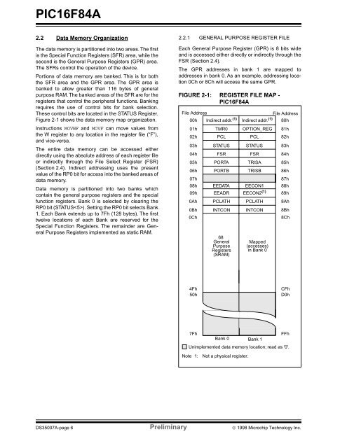
<strong>PIC16F84A</strong>2.2 <strong>Data</strong> Memory OrganizationThe data memory is partitioned into two areas. The firstis the Special Function Registers (SFR) area, while thesecond is the General Purpose Registers (GPR) area.The SFRs control the operation of the device.Portions of data memory are banked. This is for boththe SFR area and the GPR area. The GPR area isbanked to allow greater than 116 bytes of generalpurpose RAM. The banked areas of the SFR are for theregisters that control the peripheral functions. Bankingrequires the use of control bits for bank selection.These control bits are located in the STATUS Register.Figure 2-1 shows the data memory map organization.Instructions MOVWF and MOVF can move values fromthe W register to any location in the register file (“F”),and vice-versa.The entire data memory can be accessed eitherdirectly using the absolute address of each register fileor indirectly through the File Select Register (FSR)(Section 2.4). Indirect addressing uses the presentvalue of the RP0 bit for access into the banked areas ofdata memory.<strong>Data</strong> memory is partitioned into two banks whichcontain the general purpose registers and the specialfunction registers. Bank 0 is selected by clearing theRP0 bit (STATUS). Setting the RP0 bit selects Bank1. Each Bank extends up to 7Fh (128 bytes). The firsttwelve locations of each Bank are reserved for theSpecial Function Registers. The remainder are GeneralPurpose Registers implemented as static RAM.2.2.1 GENERAL PURPOSE REGISTER FILEEach General Purpose Register (GPR) is 8 bits wideand is accessed either directly or indirectly through theFSR (Section 2.4).The GPR addresses in bank 1 are mapped toaddresses in bank 0. As an example, addressing location0Ch or 8Ch will access the same GPR.FIGURE 2-1: REGISTER FILE MAP -<strong>PIC16F84A</strong>File AddressFile Address00h01h02hIndirect addr. (1)TMR0PCLIndirect addr. (1)OPTION_REGPCL80h81h82h03h04h05h06h07h08h09h0Ah0Bh0ChSTATUSFSRPORTAPORTBEEDATAEEADRPCLATHINTCON68GeneralPurposeRegisters(SRAM)STATUSFSRTRISATRISBEECON1EECON2 (1)PCLATHINTCONMapped(accesses)in Bank 083h84h85h86h87h88h89h8Ah8Bh8Ch4Fh50hCFhD0h7FhFFhBank 0 Bank 1Unimplemented data memory location; read as '0'.Note 1:Not a physical register.DS35007A-page 6 Preliminary © 1998 Microchip Technology Inc.
