

PIC16F84A 18-pin Enhanced Flash/EEPROM 8-Bit MCU Data Sheet
PIC16F84A 18-pin Enhanced Flash/EEPROM 8-Bit MCU Data Sheet
PIC16F84A 18-pin Enhanced Flash/EEPROM 8-Bit MCU Data Sheet

You also want an ePaper? Increase the reach of your titles
YUMPU automatically turns print PDFs into web optimized ePapers that Google loves.
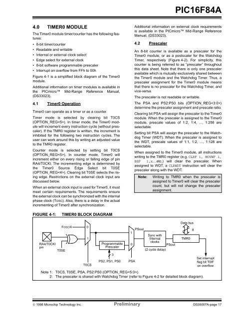
<strong>PIC16F84A</strong>4.0 TIMER0 MODULEThe Timer0 module timer/counter has the following features:• 8-bit timer/counter• Readable and writable• Internal or external clock select• Edge select for external clock• 8-bit software programmable prescaler• Interrupt on overflow from FFh to 00hFigure 4-1 is a simplified block diagram of the Timer0module.Additional information on timer modules is available inthe PICmicro Mid-Range Reference Manual,(DS33023).4.1 Timer0 OperationTimer0 can operate as a timer or as a counter.Timer mode is selected by clearing bit T0CS(OPTION_REG). In timer mode, the Timer0 modulewill increment every instruction cycle (without prescaler).If the TMR0 register is written, the increment isinhibited for the following two instruction cycles. Theuser can work around this by writing an adjusted valueto the TMR0 register.Counter mode is selected by setting bit T0CS(OPTION_REG). In counter mode, Timer0 willincrement either on every rising or falling edge of <strong>pin</strong>RA4/T0CKI. The incrementing edge is determined bythe Timer0 Source Edge Select bit T0SE(OPTION_REG). Clearing bit T0SE selects the risingedge. Restrictions on the external clock input arediscussed below.When an external clock input is used for Timer0, it mustmeet certain requirements. The requirements ensurethe external clock can be synchronized with the internalphase clock (TOSC). Also, there is a delay in the actualincrementing of Timer0 after synchronization.Additional information on external clock requirementsis available in the PICmicro Mid-Range ReferenceManual, (DS33023).4.2 PrescalerAn 8-bit counter is available as a prescaler for theTimer0 module, or as a postscaler for the WatchdogTimer, respectively (Figure 4-2). For simplicity, thiscounter is being referred to as “prescaler” throughoutthis data sheet. Note that there is only one prescaleravailable which is mutually exclusively shared betweenthe Timer0 module and the Watchdog Timer. Thus, aprescaler assignment for the Timer0 module meansthat there is no prescaler for the Watchdog Timer, andvice-versa.The prescaler is not readable or writable.The PSA and PS2:PS0 bits (OPTION_REG)determine the prescaler assignment and prescale ratio.Clearing bit PSA will assign the prescaler to the Timer0module. When the prescaler is assigned to the Timer0module, prescale values of 1:2, 1:4, ..., 1:256 areselectable.Setting bit PSA will assign the prescaler to the WatchdogTimer (WDT). When the prescaler is assigned tothe WDT, prescale values of 1:1, 1:2, ..., 1:128 areselectable.When assigned to the Timer0 module, all instructionswriting to the TMR0 register (e.g. CLRF 1, MOVWF 1,BSF 1,x....etc.) will clear the prescaler. Whenassigned to WDT, a CLRWDT instruction will clear theprescaler along with the WDT.Note:Writing to TMR0 when the prescaler isassigned to Timer0 will clear the prescalercount, but will not change the prescalerassignment.FIGURE 4-1:TIMER0 BLOCK DIAGRAMRA4/T0CKI<strong>pin</strong>T0SEFOSC/401T0CSProgrammablePrescaler3PS2, PS1, PS0Note 1: T0CS, T0SE, PSA, PS2:PS0 (OPTION_REG).2: The prescaler is shared with Watchdog Timer (refer to Figure 4-2 for detailed block diagram).10PSAPSoutSync withInternalclocksPSout(2 cycle delay)<strong>Data</strong> busTMR08Set interruptflag bit T0IFon overflow© 1998 Microchip Technology Inc. Preliminary DS35007A-page 17
