

PIC16F84A 18-pin Enhanced Flash/EEPROM 8-Bit MCU Data Sheet
PIC16F84A 18-pin Enhanced Flash/EEPROM 8-Bit MCU Data Sheet
PIC16F84A 18-pin Enhanced Flash/EEPROM 8-Bit MCU Data Sheet

You also want an ePaper? Increase the reach of your titles
YUMPU automatically turns print PDFs into web optimized ePapers that Google loves.
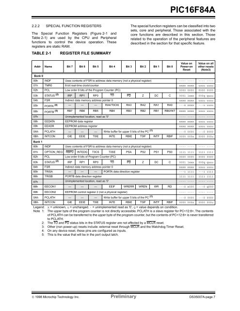
<strong>PIC16F84A</strong>2.2.2 SPECIAL FUNCTION REGISTERSThe Special Function Registers (Figure 2-1 andTable 2-1) are used by the CPU and Peripheralfunctions to control the device operation. Theseregisters are static RAM.TABLE 2-1REGISTER FILE SUMMARYThe special function registers can be classified into twosets, core and peripheral. Those associated with thecore functions are described in this section. Thoserelated to the operation of the peripheral features aredescribed in the section for that specific feature.Addr Name <strong>Bit</strong> 7 <strong>Bit</strong> 6 <strong>Bit</strong> 5 <strong>Bit</strong> 4 <strong>Bit</strong> 3 <strong>Bit</strong> 2 <strong>Bit</strong> 1 <strong>Bit</strong> 0Value onPower-onResetValue on allother resets(Note3)Bank 000h INDF Uses contents of FSR to address data memory (not a physical register) ---- ---- ---- ----01h TMR0 8-bit real-time clock/counter xxxx xxxx uuuu uuuu02h PCL Low order 8 bits of the Program Counter (PC) 0000 0000 0000 000003h STATUS (2) IRP RP1 RP0 TO PD Z DC C 0001 1xxx 000q quuu04h FSR Indirect data memory address pointer 0 xxxx xxxx uuuu uuuu05h PORTA(4) — — — RA4/T0CKI RA3 RA2 RA1 RA0 ---x xxxx ---u uuuu06h (5)PORTBRB7 RB6 RB5 RB4 RB3 RB2 RB1 RB0/INT xxxx xxxx uuuu uuuu07h Unimplemented location, read as '0' ---- ---- ---- ----08h EEDATA <strong>EEPROM</strong> data register xxxx xxxx uuuu uuuu09h EEADR <strong>EEPROM</strong> address register xxxx xxxx uuuu uuuu0Ah PCLATH — — — Write buffer for upper 5 bits of the PC (1) ---0 0000 ---0 00000Bh INTCON GIE EEIE T0IE INTE RBIE T0IF INTF RBIF 0000 000x 0000 000uBank <strong>18</strong>0h INDF Uses contents of FSR to address data memory (not a physical register) ---- ---- ---- ----81h OPTION_REG RBPU INTEDG T0CS T0SE PSA PS2 PS1 PS0 1111 1111 1111 111<strong>18</strong>2h PCL Low order 8 bits of Program Counter (PC) 0000 0000 0000 000083h STATUS (2) IRP RP1 RP0 TO PD Z DC C 0001 1xxx 000q quuu84h FSR Indirect data memory address pointer 0 xxxx xxxx uuuu uuuu85h TRISA — — — PORTA data direction register ---1 1111 ---1 111<strong>18</strong>6h TRISB PORTB data direction register 1111 1111 1111 111<strong>18</strong>7h Unimplemented location, read as '0' ---- ---- ---- ----88h EECON1 — — — EEIF WRERR WREN WR RD ---0 x000 ---0 q00089h EECON2 <strong>EEPROM</strong> control register 2 (not a physical register) ---- ---- ---- ----0Ah PCLATH — — — Write buffer for upper 5 bits of the PC (1) ---0 0000 ---0 00000Bh INTCON GIE EEIE T0IE INTE RBIE T0IF INTF RBIF 0000 000x 0000 000uLegend: x = unknown, u = unchanged. - = unimplemented read as '0', q = value depends on condition.Note 1: The upper byte of the program counter is not directly accessible. PCLATH is a slave register for PC. The contentsof PCLATH can be transferred to the upper byte of the program counter, but the contents of PC is never transferredto PCLATH.2: The TO and PD status bits in the STATUS register are not affected by a MCLR reset.3: Other (non power-up) resets include: external reset through MCLR and the Watchdog Timer Reset.4: On any device reset, these <strong>pin</strong>s are configured as inputs.5: This is the value that will be in the port output latch.© 1998 Microchip Technology Inc. Preliminary DS35007A-page 7
