<strong>PIC16F84A</strong>5.1 Reading the <strong>EEPROM</strong> <strong>Data</strong> MemoryTo read a data memory location, the user must write theaddress to the EEADR register and then set control bitRD (EECON1). The data is available, in the verynext cycle, in the EEDATA register; therefore it can beread in the next instruction. EEDATA will hold this valueuntil another read or until it is written to by the user(during a write operation).EXAMPLE 5-1:DATA <strong>EEPROM</strong> READBCF STATUS, RP0 ; Bank 0MOVLW CONFIG_ADDR ;MOVWF EEADR ; Address to readBSF STATUS, RP0 ; Bank 1BSF EECON1, RD ; EE ReadBCF STATUS, RP0 ; Bank 0MOVF EEDATA, W ; W = EEDATA5.2 Writing to the <strong>EEPROM</strong> <strong>Data</strong> MemoryTo write an <strong>EEPROM</strong> data location, the user must firstwrite the address to the EEADR register and the datato the EEDATA register. Then the user must follow aspecific sequence to initiate the write for each byte.EXAMPLE 5-1:RequiredSequenceDATA <strong>EEPROM</strong> WRITEBSF STATUS, RP0 ; Bank 1BCF INTCON, GIE ; Disable INTs.BSF EECON1, WREN ; Enable WriteMOVLW 55h ;MOVWF EECON2 ; Write 55hMOVLW AAh ;MOVWF EECON2 ; Write AAhBSF EECON1,WR ; Set WR bit; begin writeBSF INTCON, GIE ; Enable INTs.The write will not initiate if the above sequence is notexactly followed (write 55h to EECON2, write AAh toEECON2, then set WR bit) for each byte. We stronglyrecommend that interrupts be disabled during thiscode segment.Additionally, the WREN bit in EECON1 must be set toenable write. This mechanism prevents accidentalwrites to data <strong>EEPROM</strong> due to errant (unexpected)code execution (i.e., lost programs). The user shouldkeep the WREN bit clear at all times, except whenupdating <strong>EEPROM</strong>. The WREN bit is not clearedby hardwareAfter a write sequence has been initiated, clearing theWREN bit will not affect this write cycle. The WR bit willbe inhibited from being set unless the WREN bit is set.At the completion of the write cycle, the WR bit iscleared in hardware and the EE Write CompleteInterrupt Flag bit (EEIF) is set. The user can eitherenable this interrupt or poll this bit. EEIF must becleared by software.5.3 Write VerifyDepending on the application, good programming practicemay dictate that the value written to the <strong>Data</strong><strong>EEPROM</strong> should be verified (Example 5-1) to thedesired value to be written. This should be used inapplications where an <strong>EEPROM</strong> bit will be stressednear the specification limit. The Total Endurance diskwill help determine your comfort level.Generally the <strong>EEPROM</strong> write failure will be a bit whichwas written as a '0', but reads back as a '1' (due toleakage off the bit).EXAMPLE 5-1:WRITE VERIFYBCF STATUS, RP0 ; Bank 0: ; Any code can go here: ;MOVF EEDATA, W ; Must be in Bank 0BSF STATUS, RP0 ; Bank 1READBSFEECON1, RD ; YES, Read the; value writtenBCF STATUS, RP0 ; Bank 0;; Is the value written (in W reg) and; read (in EEDATA) the same?;SUBWF EEDATA, W ;BTFSS STATUS, Z ; Is difference 0?GOTO WRITE_ERR ; NO, Write error: ; YES, Good write: ; Continue programTABLE 5-1REGISTERS/BITS ASSOCIATED WITH DATA <strong>EEPROM</strong>Address Name <strong>Bit</strong> 7 <strong>Bit</strong> 6 <strong>Bit</strong> 5 <strong>Bit</strong> 4 <strong>Bit</strong> 3 <strong>Bit</strong> 2 <strong>Bit</strong> 1 <strong>Bit</strong> 0Value onPower-onResetValue on allother resets08h EEDATA <strong>EEPROM</strong> data register xxxx xxxx uuuu uuuu09h EEADR <strong>EEPROM</strong> address register xxxx xxxx uuuu uuuu88h EECON1 — — — EEIF WRERR WREN WR RD ---0 x000 ---0 q00089h EECON2 <strong>EEPROM</strong> control register 2 ---- ---- ---- ----Legend:x = unknown, u = unchanged, - = unimplemented read as '0', q = value depends upon condition. Shaded cells are notused by data <strong>EEPROM</strong>.DS35007A-page 20 Preliminary © 1998 Microchip Technology Inc.
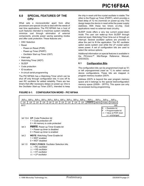
<strong>PIC16F84A</strong>6.0 SPECIAL FEATURES OF THECPUWhat sets a microcontroller apart from otherprocessors are special circuits to deal with the needs ofreal time applications. The <strong>PIC16F84A</strong> has a host ofsuch features intended to maximize system reliability,minimize cost through elimination of externalcomponents, provide power saving operating modesand offer code protection. These features are:• OSC Selection• Reset- Power-on Reset (POR)- Power-up Timer (PWRT)- Oscillator Start-up Timer (OST)• Interrupts• Watchdog Timer (WDT)• SLEEP• Code protection• ID locations• In-circuit serial programmingThe <strong>PIC16F84A</strong> has a Watchdog Timer which can beshut off only through configuration bits. It runs off itsown RC oscillator for added reliability. There are twotimers that offer necessary delays on power-up. One isthe Oscillator Start-up Timer (OST), intended to keepthe chip in reset until the crystal oscillator is stable. Theother is the Power-up Timer (PWRT), which provides afixed delay of 72 ms (nominal) on power-up only. Thisdesign keeps the device in reset while the power supplystabilizes. With these two timers on-chip, mostapplications need no external reset circuitry.SLEEP mode offers a very low current power-downmode. The user can wake-up from SLEEP throughexternal reset, Watchdog Timer time-out or through aninterrupt. Several oscillator options are provided toallow the part to fit the application. The RC oscillatoroption saves system cost while the LP crystal optionsaves power. A set of configuration bits are used toselect the various options.Additional information on special features is available inthe PICmicro Mid-Range Reference Manual,(DS33023).6.1 Configuration <strong>Bit</strong>sThe configuration bits can be programmed (read as '0')or left unprogrammed (read as '1') to select variousdevice configurations. These bits are mapped inprogram memory location 2007h.Address 2007h is beyond the user program memoryspace and it belongs to the special test/configurationmemory space (2000h - 3FFFh). This space can onlybe accessed during programming.FIGURE 6-1:CONFIGURATION WORD - <strong>PIC16F84A</strong>R/P-u R/P-u R/P-u R/P-u R/P-u R/P-u R/P-u R/P-u R/P-u R/P-u R/P-u R/P-u R/P-u R/P-uCP CP CP CP CP CP CP CP CP CP PWRTE WDTE FOSC1 FOSC0bit13bit0R = Readable bitP = Programmable bit- n = Value at POR resetu = unchangedbit 13:4 CP: Code Protection bit1 = Code protection off0 = All memory is code protectedbit 3 PWRTE: Power-up Timer Enable bit1 = Power-up timer is disabled0 = Power-up timer is enabledbit 2 WDTE: Watchdog Timer Enable bit1 = WDT enabled0 = WDT disabledbit 1:0 FOSC1:FOSC0: Oscillator Selection bits11 = RC oscillator10 = HS oscillator01 = XT oscillator00 = LP oscillator© 1998 Microchip Technology Inc. Preliminary DS35007A-page 21