

PIC16F84A 18-pin Enhanced Flash/EEPROM 8-Bit MCU Data Sheet
PIC16F84A 18-pin Enhanced Flash/EEPROM 8-Bit MCU Data Sheet
PIC16F84A 18-pin Enhanced Flash/EEPROM 8-Bit MCU Data Sheet

You also want an ePaper? Increase the reach of your titles
YUMPU automatically turns print PDFs into web optimized ePapers that Google loves.
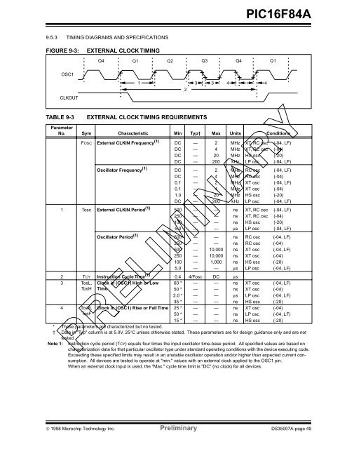
<strong>PIC16F84A</strong>9.5.3 TIMING DIAGRAMS AND SPECIFICATIONSFIGURE 9-3:EXTERNAL CLOCK TIMINGQ4 Q1 Q2 Q3 Q4 Q1OSC11 3 3 4 42CLKOUTTABLE 9-3EXTERNAL CLOCK TIMING REQUIREMENTSParameterNo. Sym Characteristic Min Typ† Max Units ConditionsFOSC External CLKIN Frequency (1) DC — 2 MHz XT, RC osc (-04, LF)DC — 4 MHz XT, RC osc (-04)DC — 20 MHz HS osc (-20)DC — 200 kHz LP osc (-04, LF)Oscillator Frequency (1) DC — 2 MHz RC osc (-04, LF)DC — 4 MHz RC osc (-04)0.1 — 2 MHz XT osc (-04, LF)0.1 — 4 MHz XT osc (-04)1.0 — 20 MHz HS osc (-20)DC — 200 kHz LP osc (-04, LF)1 Tosc External CLKIN Period (1) 500 — — ns XT, RC osc (-04, LF)250 — — ns XT, RC osc (-04)100 — — ns HS osc (-20)5.0 — — µs LP osc (-04, LF)Oscillator Period (1) 500 — — ns RC osc (-04, LF)250 — — ns RC osc (-04)500 — 10,000 ns XT osc (-04, LF)250 — 10,000 ns XT osc (-04)100 — 1,000 ns HS osc (-20)5.0 — — µs LP osc (-04, LF)2 TCY Instruction Cycle Time (1) 0.4 4/Fosc DC µs3 TosL,TosH4 TosR,TosFClock in (OSC1) High or LowTime60 * — — ns XT osc (-04, LF)50 * — — ns XT osc (-04)2.0 * — — µs LP osc (-04, LF)35 * — — ns HS osc (-20)Clock in (OSC1) Rise or Fall Time 25 * — — ns XT osc (-04)50 * — — ns LP osc (-04, LF)15 * — — ns HS osc (-20)* These parameters are characterized but no tested.† <strong>Data</strong> in "Typ" column is at 5.0V, 25°C unless otherwise stated. These parameters are for design guidance only and are nottested.Note 1: Instruction cycle period (TCY) equals four times the input oscillator time-base period. All specified values are based oncharacterization data for that particular oscillator type under standard operating conditions with the device executing code.Exceeding these specified limits may result in an unstable oscillator operation and/or higher than expected current consumption.All devices are tested to operate at "min." values with an external clock applied to the OSC1 <strong>pin</strong>.When an external clock input is used, the "Max." cycle time limit is "DC" (no clock) for all devices.© 1998 Microchip Technology Inc. Preliminary DS35007A-page 49
