

PIC16F84A 18-pin Enhanced Flash/EEPROM 8-Bit MCU Data Sheet
PIC16F84A 18-pin Enhanced Flash/EEPROM 8-Bit MCU Data Sheet
PIC16F84A 18-pin Enhanced Flash/EEPROM 8-Bit MCU Data Sheet

You also want an ePaper? Increase the reach of your titles
YUMPU automatically turns print PDFs into web optimized ePapers that Google loves.
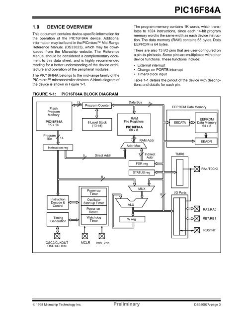
<strong>PIC16F84A</strong>1.0 DEVICE OVERVIEWThis document contains device-specific information forthe operation of the <strong>PIC16F84A</strong> device. Additionalinformation may be found in the PICmicro Mid-RangeReference Manual, (DS33023), which may be downloadedfrom the Microchip website. The ReferenceManual should be considered a complementary documentto this data sheet, and is highly recommendedreading for a better understanding of the device architectureand operation of the peripheral modules.The <strong>PIC16F84A</strong> belongs to the mid-range family of thePICmicro microcontroller devices. A block diagram ofthe device is shown in Figure 1-1.The program memory contains 1K words, which translatesto 1024 instructions, since each 14-bit programmemory word is the same width as each device instruction.The data memory (RAM) contains 68 bytes. <strong>Data</strong><strong>EEPROM</strong> is 64 bytes.There are also 13 I/O <strong>pin</strong>s that are user-configured ona <strong>pin</strong>-to-<strong>pin</strong> basis. Some <strong>pin</strong>s are multiplexed with otherdevice functions. These functions include:• External interrupt• Change on PORTB interrupt• Timer0 clock inputTable 1-1 details the <strong>pin</strong>out of the device with descriptionsand details for each <strong>pin</strong>.FIGURE 1-1:<strong>PIC16F84A</strong> BLOCK DIAGRAM<strong>Flash</strong>ProgramMemory<strong>PIC16F84A</strong>1K x 1413Program Counter8 Level Stack(13-bit)<strong>Data</strong> BusRAMFile Registers<strong>PIC16F84A</strong>68 x 88<strong>EEPROM</strong> <strong>Data</strong> MemoryEEDATA<strong>EEPROM</strong><strong>Data</strong> Memory64 x 8ProgramBus14Instruction reg7Addr MuxRAM AddrEEADR5Direct Addr7IndirectAddrTMR0FSR reg8STATUS regRA4/T0CKIInstructionDecode &ControlPower-upTimerOscillatorStart-up TimerPower-onResetALUMUX8I/O PortsRA3:RA0TimingGenerationWatchdogTimerW regRB7:RB1RB0/INTOSC2/CLKOUTOSC1/CLKINMCLRVDD, VSS© 1998 Microchip Technology Inc. Preliminary DS35007A-page 3
