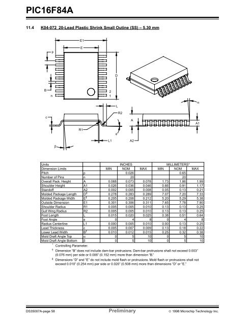
<strong>PIC16F84A</strong>11.4 K04-072 20-Lead Plastic Shrink Small Outine (SS) – 5.30 mmE1pEDB2n 1LαcR2AA1R1φβL1A2UnitsINCHESMILLIMETERS*Dimension LimitsMIN NOM MAX MIN NOM MAXPitchp0.0260.65Number of Pinsn2020Overall Pack. HeightShoulder HeightStandoffAA1A20.0680.0260.0020.0730.0360.0050.0780.0460.0081.730.660.051.860.910.131.991.170.21Molded Package Length D ‡0.278 0.283 0.289 7.07 7.20 7.33Molded Package Width E ‡0.205 0.208 0.212 5.20 5.29 5.38Outside Dimension E10.301 0.306 0.311 7.65 7.78 7.90Shoulder RadiusR10.005 0.005 0.010 0.13 0.13 0.25Gull Wing RadiusFoot LengthR2L0.0050.0150.0050.0200.0100.0250.130.380.130.510.250.64Foot Angleφ0 4 8 0 4 8Radius Centerline L10.000 0.005 0.010 0.00 0.13 0.25Lead Thicknessc0.005 0.007 0.009 0.13 0.<strong>18</strong> 0.22Lower Lead Width B †0.010 0.012 0.015 0.25 0.32 0.38Mold Draft Angle Top α0 5 10 0 5 10Mold Draft Angle Bottom β0 5 10 0 5 10* Controlling Parameter.† Dimension “B” does not include dam-bar protrusions. Dam-bar protrusions shall not exceed 0.003”(0.076 mm) per side or 0.006” (0.152 mm) more than dimension “B.”‡ Dimensions “D” and “E” do not include mold flash or protrusions. Mold flash or protrusions shall notexceed 0.010” (0.254 mm) per side or 0.020” (0.508 mm) more than dimensions “D” or “E.”DS35007A-page 58 Preliminary © 1998 Microchip Technology Inc.
<strong>PIC16F84A</strong>APPENDIX A: REVISION HISTORYVersion Date Revision DescriptionA 9/14/98 This is a new data sheet. However, the devices described in this data sheet arethe upgrades to the devices found in the PIC16F8X <strong>Data</strong> <strong>Sheet</strong>, DS30430C.APPENDIX B: CONVERSION CONSIDERATIONSConsiderations for converting from one PIC16X8Xdevice to another are listed in Table B-1.TABLE B-1:CONVERSION CONSIDERATIONS - PIC16C84, PIC16F83/F84, PIC16CR83/CR84,<strong>PIC16F84A</strong>Difference PIC16C84 PIC16F83/F84PIC16CR83/CR84<strong>PIC16F84A</strong>Program Memorysize1k x 14 512 x 14 / 1k x 14 512 x 14 / 1k x 14 1k x 14<strong>Data</strong> Memory size 36 x 8 36 x 8 / 68 x 8 36 x 8 / 68 x 8 68 x 8Voltage Range 2.0V - 6.0V(-40°C to +85°C)2.0V - 6.0V(-40°C to +85°C)2.0V - 6.0V(-40°C to +85°C)2.0V - 5.5V(-40°C to +125°C)Maximum OperatingFrequency10MHz 10MHz 10MHz 20MHzSupply Current(IDD). See parameter# D014 in theelectrical spec’s formore detail.IDD (typ) = 60µAIDD (max) = 400µA(LP osc, FOSC =32kHz, VDD = 2.0V,WDT disabled)IDD (typ) = 15µAIDD (max) = 45µA(LP osc, FOSC =32kHz, VDD = 2.0V,WDT disabled)IDD (typ) = 15µAIDD (max) = 45µA(LP osc, FOSC =32kHz, VDD = 2.0V,WDT disabled)IDD (typ) = 15µAIDD (max) = 45µA(LP osc, FOSC =32kHz, VDD = 2.0V,WDT disabled)Power-down Current(IPD). See parameters# D020, D021,and D021A in theelectrical spec’s formore detail.IPD (typ) = 26µAIPD (max) = 100µA(VDD = 2.0V, WDTdisabled, industrial)IPD (typ) = 0.4µAIPD (max) = 9µA(VDD = 2.0V, WDTdisabled, industrial)IPD (typ) = 0.4µAIPD (max) = 6µA(VDD = 2.0V, WDTdisabled, industrial)IPD (typ) = 0.4µAIPD (max) = 9µA(VDD = 2.0V, WDTdisabled, industrial)Input Low Voltage(VIL). See parameters# D032 andD034 in the electricalspec’s for moredetail.VIL (max) = 0.2VDD(Osc1, RC mode)VIL (max) = 0.1VDD(Osc1, RC mode)VIL (max) = 0.1VDD(Osc1, RC mode)VIL (max) = 0.1VDD(Osc1, RC mode)Input High Voltage(VIH). See parameter# D040 in theelectrical spec’s formore detail.VIH (min) = 0.36VDD(I/O Ports with TTL,4.5V ≤ VDD ≤ 5.5V)VIH (min) = 2.4V(I/O Ports with TTL,4.5V ≤ VDD ≤ 5.5V)VIH (min) = 2.4V(I/O Ports with TTL,4.5V ≤ VDD ≤ 5.5V)VIH (min) = 2.4V(I/O Ports with TTL,4.5V ≤ VDD ≤ 5.5V)<strong>Data</strong> <strong>EEPROM</strong>MemoryErase/Write cycletime (TDEW). Seeparameter # D122 inthe electrical spec’sfor more detail.TDEW (typ) = 10msTDEW (max) = 20msTDEW (typ) = 10msTDEW (max) = 20msTDEW (typ) = 10msTDEW (max) = 20msTDEW (typ) = 4msTDEW (max) = 10ms© 1998 Microchip Technology Inc. Preliminary DS35007A-page 59