

PIC16F84A 18-pin Enhanced Flash/EEPROM 8-Bit MCU Data Sheet
PIC16F84A 18-pin Enhanced Flash/EEPROM 8-Bit MCU Data Sheet
PIC16F84A 18-pin Enhanced Flash/EEPROM 8-Bit MCU Data Sheet

Create successful ePaper yourself
Turn your PDF publications into a flip-book with our unique Google optimized e-Paper software.
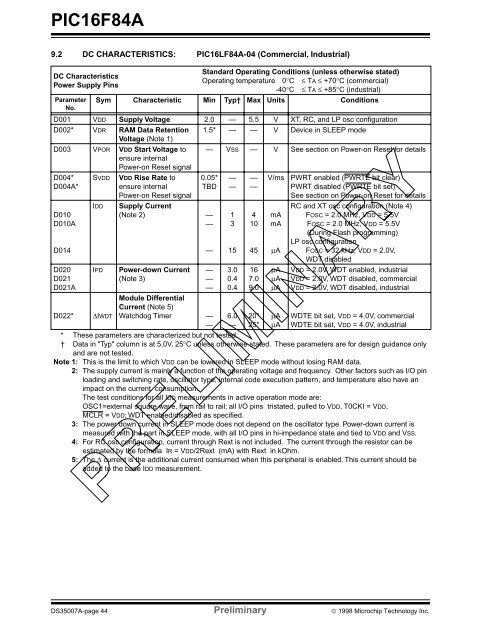
<strong>PIC16F84A</strong>9.2 DC CHARACTERISTICS: PIC16LF84A-04 (Commercial, Industrial)DC CharacteristicsPower Supply PinsParameterNo.Standard Operating Conditions (unless otherwise stated)Operating temperature 0°C ≤ TA ≤ +70°C (commercial)-40°C ≤ TA ≤ +85°C (industrial)Sym Characteristic Min Typ† Max Units ConditionsD001 VDD Supply Voltage 2.0 — 5.5 V XT, RC, and LP osc configurationD002* VDR RAM <strong>Data</strong> Retention 1.5* — — V Device in SLEEP modeVoltage (Note 1)D003 VPOR VDD Start Voltage to — VSS — V See section on Power-on Reset for detailsensure internalPower-on Reset signalD004*D004A*SVDD0.05*TBD————V/msD010D010AD014D020D021D021AIDDIPDD022* ∆IWDTVDD Rise Rate toensure internalPower-on Reset signalSupply Current(Note 2) ——Power-down Current(Note 3)————Module DifferentialCurrent (Note 5)Watchdog Timer ——13153.00.40.46.0—41045167.09.020*25*mAmAµAµAµAµAµAµAPWRT enabled (PWRTE bit clear)PWRT disabled (PWRTE bit set)See section on Power-on Reset for detailsRC and XT osc configuration (Note 4)FOSC = 2.0 MHz, VDD = 5.5VFOSC = 2.0 MHz, VDD = 5.5V(During <strong>Flash</strong> programming)LP osc configurationFOSC = 32 kHz, VDD = 2.0V,WDT disabledVDD = 2.0V, WDT enabled, industrialVDD = 2.0V, WDT disabled, commercialVDD = 2.0V, WDT disabled, industrialWDTE bit set, VDD = 4.0V, commercialWDTE bit set, VDD = 4.0V, industrial* These parameters are characterized but not tested.† <strong>Data</strong> in "Typ" column is at 5.0V, 25°C unless otherwise stated. These parameters are for design guidance onlyand are not tested.Note 1: This is the limit to which VDD can be lowered in SLEEP mode without losing RAM data.2: The supply current is mainly a function of the operating voltage and frequency. Other factors such as I/O <strong>pin</strong>loading and switching rate, oscillator type, internal code execution pattern, and temperature also have animpact on the current consumption.The test conditions for all IDD measurements in active operation mode are:OSC1=external square wave, from rail to rail; all I/O <strong>pin</strong>s tristated, pulled to VDD, T0CKI = VDD,MCLR = VDD; WDT enabled/disabled as specified.3: The power down current in SLEEP mode does not depend on the oscillator type. Power-down current ismeasured with the part in SLEEP mode, with all I/O <strong>pin</strong>s in hi-impedance state and tied to VDD and VSS.4: For RC osc configuration, current through Rext is not included. The current through the resistor can beestimated by the formula IR = VDD/2Rext (mA) with Rext in kOhm.5: The ∆ current is the additional current consumed when this peripheral is enabled. This current should beadded to the base IDD measurement.DS35007A-page 44 Preliminary © 1998 Microchip Technology Inc.
