

PIC16F84A 18-pin Enhanced Flash/EEPROM 8-Bit MCU Data Sheet
PIC16F84A 18-pin Enhanced Flash/EEPROM 8-Bit MCU Data Sheet
PIC16F84A 18-pin Enhanced Flash/EEPROM 8-Bit MCU Data Sheet

Create successful ePaper yourself
Turn your PDF publications into a flip-book with our unique Google optimized e-Paper software.
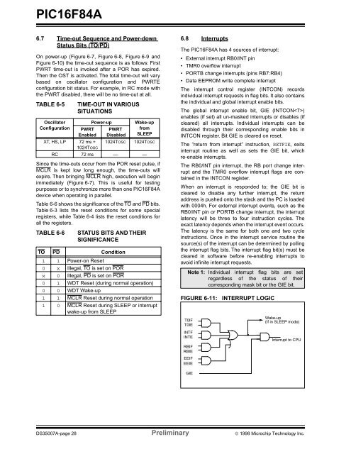
<strong>PIC16F84A</strong>6.7 Time-out Sequence and Power-downStatus <strong>Bit</strong>s (TO/PD)On power-up (Figure 6-7, Figure 6-8, Figure 6-9 andFigure 6-10) the time-out sequence is as follows: FirstPWRT time-out is invoked after a POR has expired.Then the OST is activated. The total time-out will varybased on oscillator configuration and PWRTEconfiguration bit status. For example, in RC mode withthe PWRT disabled, there will be no time-out at all.TABLE 6-5OscillatorConfigurationTIME-OUT IN VARIOUSSITUATIONSSince the time-outs occur from the POR reset pulse, ifMCLR is kept low long enough, the time-outs willexpire. Then bringing MCLR high, execution will beginimmediately (Figure 6-7). This is useful for testingpurposes or to synchronize more than one <strong>PIC16F84A</strong>device when operating in parallel.Table 6-6 shows the significance of the TO and PD bits.Table 6-3 lists the reset conditions for some specialregisters, while Table 6-4 lists the reset conditions forall the registers.TABLE 6-6PWRTEnabledXT, HS, LP 72 ms +1024TOSCPower-upPWRTDisabled1024TOSCWake-upfromSLEEP1024TOSCRC 72 ms — —STATUS BITS AND THEIRSIGNIFICANCETO PD Condition1 1 Power-on Reset0 x Illegal, TO is set on PORx 0 Illegal, PD is set on POR0 1 WDT Reset (during normal operation)0 0 WDT Wake-up1 1 MCLR Reset during normal operation1 0 MCLR Reset during SLEEP or interruptwake-up from SLEEP6.8 InterruptsThe <strong>PIC16F84A</strong> has 4 sources of interrupt:• External interrupt RB0/INT <strong>pin</strong>• TMR0 overflow interrupt• PORTB change interrupts (<strong>pin</strong>s RB7:RB4)• <strong>Data</strong> <strong>EEPROM</strong> write complete interruptThe interrupt control register (INTCON) recordsindividual interrupt requests in flag bits. It also containsthe individual and global interrupt enable bits.The global interrupt enable bit, GIE (INTCON)enables (if set) all un-masked interrupts or disables (ifcleared) all interrupts. Individual interrupts can bedisabled through their corresponding enable bits inINTCON register. <strong>Bit</strong> GIE is cleared on reset.The “return from interrupt” instruction, RETFIE, exitsinterrupt routine as well as sets the GIE bit, whichre-enable interrupts.The RB0/INT <strong>pin</strong> interrupt, the RB port change interruptand the TMR0 overflow interrupt flags are containedin the INTCON register.When an interrupt is responded to; the GIE bit iscleared to disable any further interrupt, the returnaddress is pushed onto the stack and the PC is loadedwith 0004h. For external interrupt events, such as theRB0/INT <strong>pin</strong> or PORTB change interrupt, the interruptlatency will be three to four instruction cycles. Theexact latency depends when the interrupt event occurs.The latency is the same for both one and two cycleinstructions. Once in the interrupt service routine thesource(s) of the interrupt can be determined by pollingthe interrupt flag bits. The interrupt flag bit(s) must becleared in software before re-enabling interrupts toavoid infinite interrupt requests.Note 1: Individual interrupt flag bits are setregardless of the status of theircorresponding mask bit or the GIE bit.FIGURE 6-11:T0IFT0IEINTFINTERBIFRBIEEEIFEEIEINTERRUPT LOGICWake-up(If in SLEEP mode)Interrupt to CPUGIEDS35007A-page 28 Preliminary © 1998 Microchip Technology Inc.
