

PIC16F84A 18-pin Enhanced Flash/EEPROM 8-Bit MCU Data Sheet
PIC16F84A 18-pin Enhanced Flash/EEPROM 8-Bit MCU Data Sheet
PIC16F84A 18-pin Enhanced Flash/EEPROM 8-Bit MCU Data Sheet

Create successful ePaper yourself
Turn your PDF publications into a flip-book with our unique Google optimized e-Paper software.
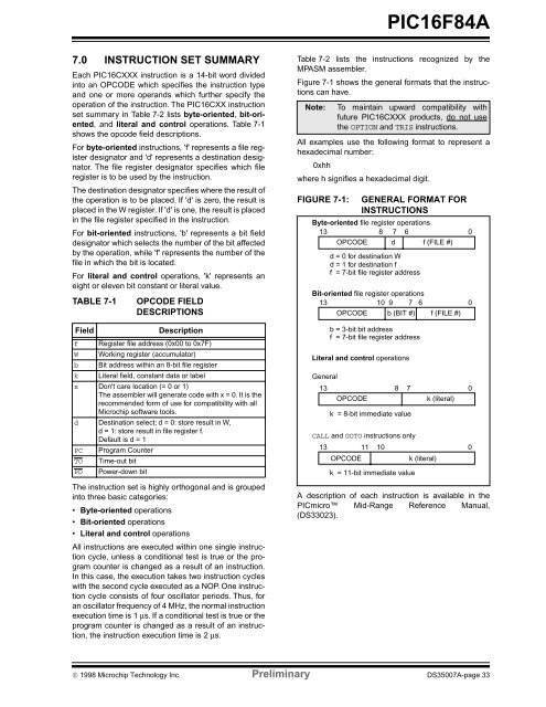
<strong>PIC16F84A</strong>7.0 INSTRUCTION SET SUMMARYEach PIC16CXXX instruction is a 14-bit word dividedinto an OPCODE which specifies the instruction typeand one or more operands which further specify theoperation of the instruction. The PIC16CXX instructionset summary in Table 7-2 lists byte-oriented, bit-oriented,and literal and control operations. Table 7-1shows the opcode field descriptions.For byte-oriented instructions, 'f' represents a file registerdesignator and 'd' represents a destination designator.The file register designator specifies which fileregister is to be used by the instruction.The destination designator specifies where the result ofthe operation is to be placed. If 'd' is zero, the result isplaced in the W register. If 'd' is one, the result is placedin the file register specified in the instruction.For bit-oriented instructions, 'b' represents a bit fielddesignator which selects the number of the bit affectedby the operation, while 'f' represents the number of thefile in which the bit is located.For literal and control operations, 'k' represents aneight or eleven bit constant or literal value.TABLE 7-1FieldOPCODE FIELDDESCRIPTIONSDescriptionf Register file address (0x00 to 0x7F)W Working register (accumulator)b <strong>Bit</strong> address within an 8-bit file registerk Literal field, constant data or labelx Don't care location (= 0 or 1)The assembler will generate code with x = 0. It is therecommended form of use for compatibility with allMicrochip software tools.d Destination select; d = 0: store result in W,d = 1: store result in file register f.Default is d = 1PC Program CounterTO Time-out bitPD Power-down bitThe instruction set is highly orthogonal and is groupedinto three basic categories:• Byte-oriented operations• <strong>Bit</strong>-oriented operations• Literal and control operationsAll instructions are executed within one single instructioncycle, unless a conditional test is true or the programcounter is changed as a result of an instruction.In this case, the execution takes two instruction cycleswith the second cycle executed as a NOP. One instructioncycle consists of four oscillator periods. Thus, foran oscillator frequency of 4 MHz, the normal instructionexecution time is 1 µs. If a conditional test is true or theprogram counter is changed as a result of an instruction,the instruction execution time is 2 µs.Table 7-2 lists the instructions recognized by theMPASM assembler.Figure 7-1 shows the general formats that the instructionscan have.Note:All examples use the following format to represent ahexadecimal number:0xhhwhere h signifies a hexadecimal digit.FIGURE 7-1:To maintain upward compatibility withfuture PIC16CXXX products, do not usethe OPTION and TRIS instructions.GENERAL FORMAT FORINSTRUCTIONSByte-oriented file register operations13 8 7 6 0OPCODE d f (FILE #)d = 0 for destination Wd = 1 for destination ff = 7-bit file register address<strong>Bit</strong>-oriented file register operations13 10 9 7 6 0OPCODE b (BIT #) f (FILE #)b = 3-bit bit addressf = 7-bit file register addressLiteral and control operationsGeneral13 8 7 0OPCODEk (literal)k = 8-bit immediate valueCALL and GOTO instructions only13 11 10 0OPCODEk (literal)k = 11-bit immediate valueA description of each instruction is available in thePICmicro Mid-Range Reference Manual,(DS33023).© 1998 Microchip Technology Inc. Preliminary DS35007A-page 33
