

PIC16F84A 18-pin Enhanced Flash/EEPROM 8-Bit MCU Data Sheet
PIC16F84A 18-pin Enhanced Flash/EEPROM 8-Bit MCU Data Sheet
PIC16F84A 18-pin Enhanced Flash/EEPROM 8-Bit MCU Data Sheet

Create successful ePaper yourself
Turn your PDF publications into a flip-book with our unique Google optimized e-Paper software.
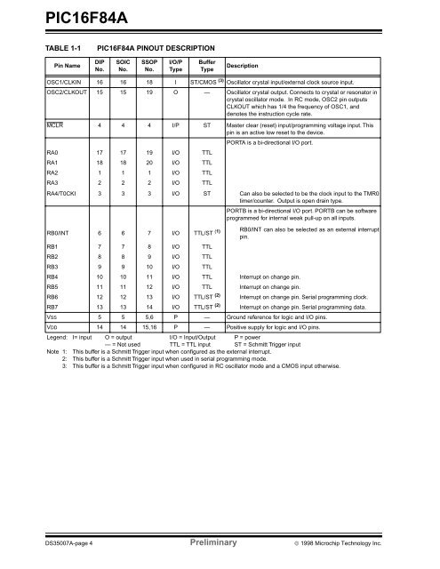
<strong>PIC16F84A</strong>TABLE 1-1<strong>PIC16F84A</strong> PINOUT DESCRIPTIONPin NameDIPNo.SOICNo.SSOPNo.I/O/PTypeBufferTypeDescriptionOSC1/CLKIN 16 16 <strong>18</strong> I ST/CMOS (3) Oscillator crystal input/external clock source input.OSC2/CLKOUT 15 15 19 O — Oscillator crystal output. Connects to crystal or resonator incrystal oscillator mode. In RC mode, OSC2 <strong>pin</strong> outputsCLKOUT which has 1/4 the frequency of OSC1, anddenotes the instruction cycle rate.MCLR 4 4 4 I/P ST Master clear (reset) input/programming voltage input. This<strong>pin</strong> is an active low reset to the device.PORTA is a bi-directional I/O port.RA0 17 17 19 I/O TTLRA1 <strong>18</strong> <strong>18</strong> 20 I/O TTLRA2 1 1 1 I/O TTLRA3 2 2 2 I/O TTLRA4/T0CKI 3 3 3 I/O ST Can also be selected to be the clock input to the TMR0timer/counter. Output is open drain type.PORTB is a bi-directional I/O port. PORTB can be softwareprogrammed for internal weak pull-up on all inputs.RB0/INT 6 6 7 I/O TTL/ST (1) RB0/INT can also be selected as an external interrupt<strong>pin</strong>.RB1 7 7 8 I/O TTLRB2 8 8 9 I/O TTLRB3 9 9 10 I/O TTLRB4 10 10 11 I/O TTL Interrupt on change <strong>pin</strong>.RB5 11 11 12 I/O TTL Interrupt on change <strong>pin</strong>.RB6 12 12 13 I/O TTL/ST (2) Interrupt on change <strong>pin</strong>. Serial programming clock.RB7 13 13 14 I/O TTL/ST (2) Interrupt on change <strong>pin</strong>. Serial programming data.VSS 5 5 5,6 P — Ground reference for logic and I/O <strong>pin</strong>s.VDD 14 14 15,16 P — Positive supply for logic and I/O <strong>pin</strong>s.Legend: I= input O = output I/O = Input/Output P = power— = Not used TTL = TTL input ST = Schmitt Trigger inputNote 1: This buffer is a Schmitt Trigger input when configured as the external interrupt.2: This buffer is a Schmitt Trigger input when used in serial programming mode.3: This buffer is a Schmitt Trigger input when configured in RC oscillator mode and a CMOS input otherwise.DS35007A-page 4 Preliminary © 1998 Microchip Technology Inc.
