

PIC16F84A 18-pin Enhanced Flash/EEPROM 8-Bit MCU Data Sheet
PIC16F84A 18-pin Enhanced Flash/EEPROM 8-Bit MCU Data Sheet
PIC16F84A 18-pin Enhanced Flash/EEPROM 8-Bit MCU Data Sheet

You also want an ePaper? Increase the reach of your titles
YUMPU automatically turns print PDFs into web optimized ePapers that Google loves.
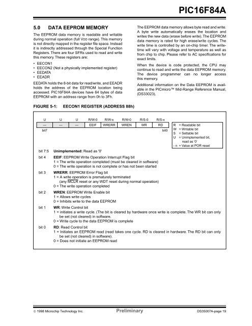
<strong>PIC16F84A</strong>5.0 DATA <strong>EEPROM</strong> MEMORYThe <strong>EEPROM</strong> data memory is readable and writableduring normal operation (full VDD range). This memoryis not directly mapped in the register file space. Insteadit is indirectly addressed through the Special FunctionRegisters. There are four SFRs used to read and writethis memory. These registers are:• EECON1• EECON2 (Not a physically implemented register)• EEDATA• EEADREEDATA holds the 8-bit data for read/write, and EEADRholds the address of the <strong>EEPROM</strong> location beingaccessed. <strong>PIC16F84A</strong> devices have 64 bytes of data<strong>EEPROM</strong> with an address range from 0h to 3Fh.The <strong>EEPROM</strong> data memory allows byte read and write.A byte write automatically erases the location andwrites the new data (erase before write). The <strong>EEPROM</strong>data memory is rated for high erase/write cycles. Thewrite time is controlled by an on-chip timer. The writetimewill vary with voltage and temperature as well asfrom chip to chip. Please refer to AC specifications forexact limits.When the device is code protected, the CPU maycontinue to read and write the data <strong>EEPROM</strong> memory.The device programmer can no longer accessthis memory.Additional information on the <strong>Data</strong> <strong>EEPROM</strong> is availablein the PICmicro Mid-Range Reference Manual,(DS33023).FIGURE 5-1: EECON1 REGISTER (ADDRESS 88h)U U U R/W-0 R/W-x R/W-0 R/S-0 R/S-x— — — EEIF WRERR WREN WR RD R = Readable bitbit7bit0 W = Writable bitS = Settable bitU = Unimplemented bit,read as ‘0’- n = Value at POR resetbit 7:5bit 4bit 3bit 2bit 1bit 0Unimplemented: Read as '0'EEIF: <strong>EEPROM</strong> Write Operation Interrupt Flag bit1 = The write operation completed (must be cleared in software)0 = The write operation is not complete or has not been startedWRERR: <strong>EEPROM</strong> Error Flag bit1 = A write operation is prematurely terminated(any MCLR reset or any WDT reset during normal operation)0 = The write operation completedWREN: <strong>EEPROM</strong> Write Enable bit1 = Allows write cycles0 = Inhibits write to the data <strong>EEPROM</strong>WR: Write Control bit1 = initiates a write cycle. (The bit is cleared by hardware once write is complete. The WR bit can onlybe set (not cleared) in software.0 = Write cycle to the data <strong>EEPROM</strong> is completeRD: Read Control bit1 = Initiates an <strong>EEPROM</strong> read (read takes one cycle. RD is cleared in hardware. The RD bit can onlybe set (not cleared) in software).0 = Does not initiate an <strong>EEPROM</strong> read© 1998 Microchip Technology Inc. Preliminary DS35007A-page 19
