

PIC16F84A 18-pin Enhanced Flash/EEPROM 8-Bit MCU Data Sheet
PIC16F84A 18-pin Enhanced Flash/EEPROM 8-Bit MCU Data Sheet
PIC16F84A 18-pin Enhanced Flash/EEPROM 8-Bit MCU Data Sheet

Create successful ePaper yourself
Turn your PDF publications into a flip-book with our unique Google optimized e-Paper software.
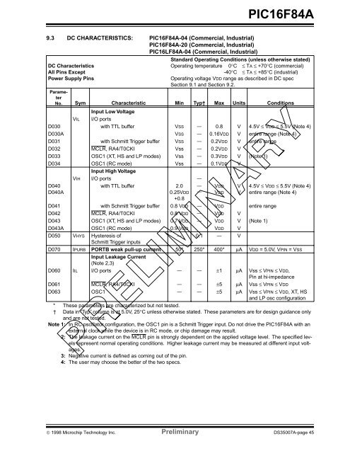
<strong>PIC16F84A</strong>9.3 DC CHARACTERISTICS: <strong>PIC16F84A</strong>-04 (Commercial, Industrial)<strong>PIC16F84A</strong>-20 (Commercial, Industrial)PIC16LF84A-04 (Commercial, Industrial)DC CharacteristicsAll Pins ExceptPower Supply PinsStandard Operating Conditions (unless otherwise stated)Operating temperature 0°C ≤ TA ≤ +70°C (commercial)-40°C ≤ TA ≤ +85°C (industrial)Operating voltage VDD range as described in DC specSection 9.1 and Section 9.2.ParameterNo. Sym Characteristic Min Typ† Max Units ConditionsInput Low VoltageVIL I/O portsD030 with TTL buffer VSS — 0.8 V 4.5V ≤ VDD ≤ 5.5V (Note 4)D030A VSS — 0.16VDD V entire range (Note 4)D031 with Schmitt Trigger buffer VSS — 0.2VDD V entire rangeD032 MCLR, RA4/T0CKI Vss — 0.2VDD VD033 OSC1 (XT, HS and LP modes) Vss — 0.3VDD V (Note 1)D034 OSC1 (RC mode) Vss — 0.1VDD VInput High VoltageVIH I/O ports —D040D040Awith TTL buffer 2.00.25VDD+0.8——VDDVDDVV4.5V ≤ VDD ≤ 5.5V (Note 4)entire range (Note 4)D041 with Schmitt Trigger buffer 0.8 VDD — VDD entire rangeD042 MCLR, RA4/T0CKI 0.8 VDD — VDD VD043 OSC1 (XT, HS and LP modes) 0.7 VDD — VDD V (Note 1)D043A OSC1 (RC mode) 0.9 VDD VDD VD050 VHYS Hysteresis of— 0.1 — VSchmitt Trigger inputsD070 IPURB PORTB weak pull-up current 50* 250* 400* µA VDD = 5.0V, VPIN = VSSInput Leakage Current(Note 2,3)D060 IIL I/O ports — — ±1 µA Vss ≤ VPIN ≤ VDD,Pin at hi-impedanceD061 MCLR, RA4/T0CKI — — ±5 µA Vss ≤ VPIN ≤ VDDD063 OSC1 — — ±5 µA Vss ≤ VPIN ≤ VDD, XT, HSand LP osc configuration* These parameters are characterized but not tested.† <strong>Data</strong> in “Typ” column is at 5.0V, 25°C unless otherwise stated. These parameters are for design guidance onlyand are not tested.Note 1: In RC oscillator configuration, the OSC1 <strong>pin</strong> is a Schmitt Trigger input. Do not drive the <strong>PIC16F84A</strong> with anexternal clock while the device is in RC mode, or chip damage may result.2: The leakage current on the MCLR <strong>pin</strong> is strongly dependent on the applied voltage level. The specified levelsrepresent normal operating conditions. Higher leakage current may be measured at different input voltages.3: Negative current is defined as coming out of the <strong>pin</strong>.4: The user may choose the better of the two specs.© 1998 Microchip Technology Inc. Preliminary DS35007A-page 45
