

PIC16F84A 18-pin Enhanced Flash/EEPROM 8-Bit MCU Data Sheet
PIC16F84A 18-pin Enhanced Flash/EEPROM 8-Bit MCU Data Sheet
PIC16F84A 18-pin Enhanced Flash/EEPROM 8-Bit MCU Data Sheet

You also want an ePaper? Increase the reach of your titles
YUMPU automatically turns print PDFs into web optimized ePapers that Google loves.
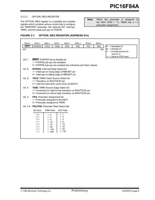
<strong>PIC16F84A</strong>2.2.2.2 OPTION_REG REGISTERThe OPTION_REG register is a readable and writableregister which contains various control bits to configurethe TMR0/WDT prescaler, the external INT interrupt,TMR0, and the weak pull-ups on PORTB.Note:When the prescaler is assigned tothe WDT (PSA = '1'), TMR0 has a 1:1prescaler assignment.FIGURE 2-1: OPTION_REG REGISTER (ADDRESS 81h)R/W-1 R/W-1 R/W-1 R/W-1 R/W-1 R/W-1 R/W-1 R/W-1RBPU INTEDG T0CS T0SE PSA PS2 PS1 PS0 R = Readable bitbit7bit0 W = Writable bitU = Unimplemented bit,read as ‘0’- n = Value at POR resetbit 7: RBPU: PORTB Pull-up Enable bit1 = PORTB pull-ups are disabled0 = PORTB pull-ups are enabled (by individual port latch values)bit 6: INTEDG: Interrupt Edge Select bit1 = Interrupt on rising edge of RB0/INT <strong>pin</strong>0 = Interrupt on falling edge of RB0/INT <strong>pin</strong>bit 5: T0CS: TMR0 Clock Source Select bit1 = Transition on RA4/T0CKI <strong>pin</strong>0 = Internal instruction cycle clock (CLKOUT)bit 4: T0SE: TMR0 Source Edge Select bit1 = Increment on high-to-low transition on RA4/T0CKI <strong>pin</strong>0 = Increment on low-to-high transition on RA4/T0CKI <strong>pin</strong>bit 3: PSA: Prescaler Assignment bit1 = Prescaler assigned to the WDT0 = Prescaler assigned to TMR0bit 2-0: PS2:PS0: Prescaler Rate Select bits<strong>Bit</strong> Value TMR0 Rate WDT Rate0000010100111001011101111 : 21 : 41 : 81 : 161 : 321 : 641 : 1281 : 2561 : 11 : 21 : 41 : 81 : 161 : 321 : 641 : 128© 1998 Microchip Technology Inc. Preliminary DS35007A-page 9
