

PIC16F84A 18-pin Enhanced Flash/EEPROM 8-Bit MCU Data Sheet
PIC16F84A 18-pin Enhanced Flash/EEPROM 8-Bit MCU Data Sheet
PIC16F84A 18-pin Enhanced Flash/EEPROM 8-Bit MCU Data Sheet

Create successful ePaper yourself
Turn your PDF publications into a flip-book with our unique Google optimized e-Paper software.
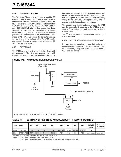
<strong>PIC16F84A</strong>6.10 Watchdog Timer (WDT)The Watchdog Timer is a free running on-chip RCoscillator which does not require any externalcomponents. This RC oscillator is separate from theRC oscillator of the OSC1/CLKIN <strong>pin</strong>. That means thatthe WDT will run even if the clock on the OSC1/CLKINand OSC2/CLKOUT <strong>pin</strong>s of the device has beenstopped, for example, by execution of a SLEEPinstruction. During normal operation a WDT time-outgenerates a device RESET. If the device is in SLEEPmode, a WDT Wake-up causes the device to wake-upand continue with normal operation. The WDT can bepermanently disabled by programming configuration bitWDTE as a '0' (Section 6.1).6.10.1 WDT PERIODThe WDT has a nominal time-out period of <strong>18</strong> ms, (withno prescaler). The time-out periods vary withtemperature, VDD and process variations from part topart (see DC specs). If longer time-out periods aredesired, a prescaler with a division ratio of up to 1:128can be assigned to the WDT under software control bywriting to the OPTION_REG register. Thus, time-outperiods up to 2.3 seconds can be realized.The CLRWDT and SLEEP instructions clear the WDTand the postscaler (if assigned to the WDT) and preventit from timing out and generating a deviceRESET condition.The TO bit in the STATUS register will be cleared upona WDT time-out.6.10.2 WDT PROGRAMMING CONSIDERATIONSIt should also be taken into account that under worstcase conditions (VDD = Min., Temperature = Max., max.WDT prescaler) it may take several seconds before aWDT time-out occurs.FIGURE 6-12:WATCHDOG TIMER BLOCK DIAGRAMFrom TMR0 Clock Source(Figure 4-2)WDT Timer01•MUXPostscaler88 - to -1 MUXPS2:PS0WDTEnable <strong>Bit</strong>PSA•To TMR0 (Figure 4-2)01MUXPSAWDTTime-outNote: PSA and PS2:PS0 are bits in the OPTION_REG register.TABLE 6-7SUMMARY OF REGISTERS ASSOCIATED WITH THE WATCHDOG TIMERAddr Name <strong>Bit</strong> 7 <strong>Bit</strong> 6 <strong>Bit</strong> 5 <strong>Bit</strong> 4 <strong>Bit</strong> 3 <strong>Bit</strong> 2 <strong>Bit</strong> 1 <strong>Bit</strong> 0Value onPower-onResetValue on allother resets2007h Config. bits (2) (2) (2) (2) PWRTE (1) WDTE FOSC1 FOSC0 (2)81h OPTION_REG RBPU INTEDG T0CS T0SE PSA PS2 PS1 PS0 1111 1111 1111 1111Legend: x = unknown. Shaded cells are not used by the WDT.Note 1: See Figure 6-1 for operation of the PWRTE bit.2: See Figure 6-1 and Section 6.12 for operation of the Code and <strong>Data</strong> protection bits.DS35007A-page 30 Preliminary © 1998 Microchip Technology Inc.
