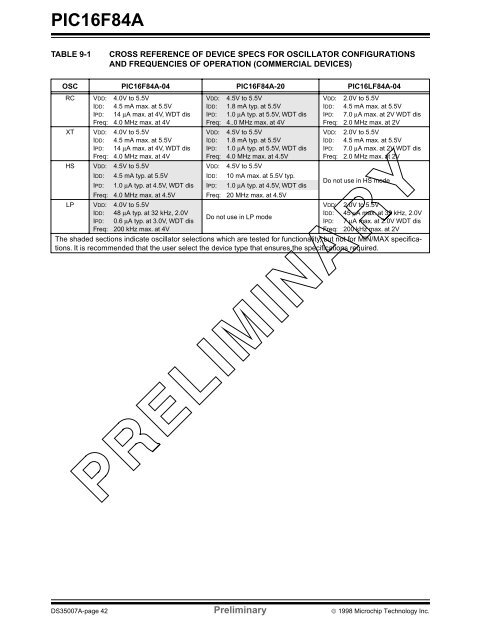
<strong>PIC16F84A</strong>TABLE 9-1CROSS REFERENCE OF DEVICE SPECS FOR OSCILLATOR CONFIGURATIONSAND FREQUENCIES OF OPERATION (COMMERCIAL DEVICES)OSC <strong>PIC16F84A</strong>-04 <strong>PIC16F84A</strong>-20 PIC16LF84A-04RC VDD: 4.0V to 5.5VVDD: 4.5V to 5.5VVDD: 2.0V to 5.5VIDD: 4.5 mA max. at 5.5VIDD: 1.8 mA typ. at 5.5VIDD: 4.5 mA max. at 5.5VIPD: 14 µA max. at 4V, WDT dis IPD: 1.0 µA typ. at 5.5V, WDT dis IPD: 7.0 µA max. at 2V WDT disFreq: 4.0 MHz max. at 4VFreq: 4..0 MHz max. at 4VFreq: 2.0 MHz max. at 2VXT VDD: 4.0V to 5.5VVDD: 4.5V to 5.5VVDD: 2.0V to 5.5VIDD: 4.5 mA max. at 5.5VIDD: 1.8 mA typ. at 5.5VIDD: 4.5 mA max. at 5.5VIPD: 14 µA max. at 4V, WDT dis IPD: 1.0 µA typ. at 5.5V, WDT dis IPD: 7.0 µA max. at 2V WDT disFreq: 4.0 MHz max. at 4VFreq: 4.0 MHz max. at 4.5VFreq: 2.0 MHz max. at 2VHS VDD: 4.5V to 5.5V VDD: 4.5V to 5.5VIDD: 4.5 mA typ. at 5.5V IDD: 10 mA max. at 5.5V typ.IPD: 1.0 µA typ. at 4.5V, WDT dis IPD: 1.0 µA typ. at 4.5V, WDT disDo not use in HS modeFreq: 4.0 MHz max. at 4.5V Freq: 20 MHz max. at 4.5VLP VDD: 4.0V to 5.5VVDD: 2.0V to 5.5VIDD: 48 µA typ. at 32 kHz, 2.0VIDD: 45 µA max. at 32 kHz, 2.0VDo not use in LP modeIPD: 0.6 µA typ. at 3.0V, WDT disIPD: 7 µA max. at 2.0V WDT disFreq: 200 kHz max. at 4VFreq: 200 kHz max. at 2VThe shaded sections indicate oscillator selections which are tested for functionality, but not for MIN/MAX specifications.It is recommended that the user select the device type that ensures the specifications required.DS35007A-page 42 Preliminary © 1998 Microchip Technology Inc.
<strong>PIC16F84A</strong>9.1 DC CHARACTERISTICS: <strong>PIC16F84A</strong>-04 (Commercial, Industrial)<strong>PIC16F84A</strong>-20 (Commercial, Industrial)DC CharacteristicsPower Supply PinsParameterNo.D001D001AStandard Operating Conditions (unless otherwise stated)Operating temperature 0°C ≤ TA ≤ +70°C (commercial)-40°C ≤ TA ≤ +85°C (industrial)Sym Characteristic Min Typ† Max Units ConditionsVDD Supply Voltage 4.04.5D002* VDR RAM <strong>Data</strong> RetentionVoltage (Note 1)D003 VPOR VDD Start Voltage toensure internalPower-on Reset signalD004*D004A*D010D010AD013D020D021D021ASVDDIDDIPDD022* ∆IWDTVDD Rise Rate toensure internalPower-on Reset signal——5.55.5VVXT, RC and LP osc configurationHS osc configuration1.5* — — V Device in SLEEP mode— VSS — V See section on Power-on Reset for details0.05*TBDSupply Current(Note 2) ——Power-down Current(Note 3)————Module DifferentialCurrent (Note 5)Watchdog Timer ————1.83107.01.01.06.0———4.5102028141620*25*V/msmAmAmAµAµAµAµAµAPWRT enabled (PWRTE bit clear)PWRT disabled (PWRTE bit set)See section on Power-on Reset for detailsRC and XT osc configuration (Note 4)FOSC = 4.0 MHz, VDD = 5.5VFOSC = 4.0 MHz, VDD = 5.5V(During <strong>Flash</strong> programming)HS osc configuration (<strong>PIC16F84A</strong>-20)FOSC = 20 MHz, VDD = 5.5VVDD = 4.0V, WDT enabled, industrialVDD = 4.0V, WDT disabled, commercialVDD = 4.0V, WDT disabled, industrialWDTE bit set, VDD = 4.0V, commercialWDTE bit set, VDD = 4.0V, extended* These parameters are characterized but not tested.† <strong>Data</strong> in "Typ" column is at 5.0V, 25˚C unless otherwise stated. These parameters are for design guidance onlyand are not tested.Note 1: This is the limit to which VDD can be lowered without losing RAM data.2: The supply current is mainly a function of the operating voltage and frequency. Other factors such as I/O <strong>pin</strong>loading and switching rate, oscillator type, internal code execution pattern, and temperature also have animpact on the current consumption.The test conditions for all IDD measurements in active operation mode are:OSC1=external square wave, from rail to rail; all I/O <strong>pin</strong>s tristated, pulled to VDD, T0CKI = VDD,MCLR = VDD; WDT enabled/disabled as specified.3: The power down current in SLEEP mode does not depend on the oscillator type. Power-down current ismeasured with the part in SLEEP mode, with all I/O <strong>pin</strong>s in hi-impedance state and tied to VDD and VSS.4: For RC osc configuration, current through Rext is not included. The current through the resistor can be estimatedby the formula IR = VDD/2Rext (mA) with Rext in kOhm.5: The ∆ current is the additional current consumed when this peripheral is enabled. This current should beadded to the base IDD measurement.© 1998 Microchip Technology Inc. Preliminary DS35007A-page 43