

PIC16F84A 18-pin Enhanced Flash/EEPROM 8-Bit MCU Data Sheet
PIC16F84A 18-pin Enhanced Flash/EEPROM 8-Bit MCU Data Sheet
PIC16F84A 18-pin Enhanced Flash/EEPROM 8-Bit MCU Data Sheet

You also want an ePaper? Increase the reach of your titles
YUMPU automatically turns print PDFs into web optimized ePapers that Google loves.
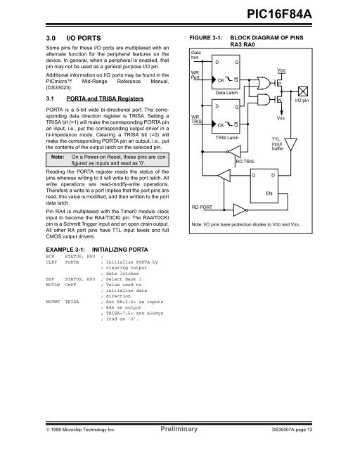
<strong>PIC16F84A</strong>3.0 I/O PORTSSome <strong>pin</strong>s for these I/O ports are multiplexed with analternate function for the peripheral features on thedevice. In general, when a peripheral is enabled, that<strong>pin</strong> may not be used as a general purpose I/O <strong>pin</strong>.Additional information on I/O ports may be found in thePICmicro Mid-Range Reference Manual,(DS33023).3.1 PORTA and TRISA RegistersPORTA is a 5-bit wide bi-directional port. The correspondingdata direction register is TRISA. Setting aTRISA bit (=1) will make the corresponding PORTA <strong>pin</strong>an input, i.e., put the corresponding output driver in ahi-impedance mode. Clearing a TRISA bit (=0) willmake the corresponding PORTA <strong>pin</strong> an output, i.e., putthe contents of the output latch on the selected <strong>pin</strong>.Note:On a Power-on Reset, these <strong>pin</strong>s are configuredas inputs and read as '0'.Reading the PORTA register reads the status of the<strong>pin</strong>s whereas writing to it will write to the port latch. Allwrite operations are read-modify-write operations.Therefore a write to a port implies that the port <strong>pin</strong>s areread, this value is modified, and then written to the portdata latch.Pin RA4 is multiplexed with the Timer0 module clockinput to become the RA4/T0CKI <strong>pin</strong>. The RA4/T0CKI<strong>pin</strong> is a Schmitt Trigger input and an open drain output.All other RA port <strong>pin</strong>s have TTL input levels and fullCMOS output drivers.FIGURE 3-1:<strong>Data</strong>busWRPortWRTRISRD PORTDDCKCKBLOCK DIAGRAM OF PINSRA3:RA0QQ<strong>Data</strong> LatchQQTRIS LatchRD TRISNote: I/O <strong>pin</strong>s have protection diodes to VDD and VSS.QENDVDDPNVSSTTLinputbufferI/O <strong>pin</strong>EXAMPLE 3-1: INITIALIZING PORTABCF STATUS, RP0 ;CLRF PORTA ; Initialize PORTA by; clearing output; data latchesBSF STATUS, RP0 ; Select Bank 1MOVLW 0x0F; Value used to; initialize data; directionMOVWF TRISA ; Set RA as inputs; RA4 as output; TRISA are always; read as '0'.© 1998 Microchip Technology Inc. Preliminary DS35007A-page 13
