

PIC16F84A 18-pin Enhanced Flash/EEPROM 8-Bit MCU Data Sheet
PIC16F84A 18-pin Enhanced Flash/EEPROM 8-Bit MCU Data Sheet
PIC16F84A 18-pin Enhanced Flash/EEPROM 8-Bit MCU Data Sheet

Create successful ePaper yourself
Turn your PDF publications into a flip-book with our unique Google optimized e-Paper software.
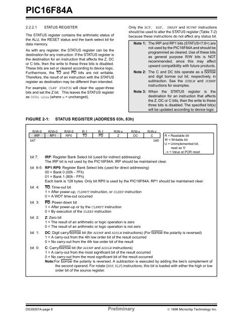
<strong>PIC16F84A</strong>2.2.2.1 STATUS REGISTERThe STATUS register contains the arithmetic status ofthe ALU, the RESET status and the bank select bit fordata memory.As with any register, the STATUS register can be thedestination for any instruction. If the STATUS register isthe destination for an instruction that affects the Z, DCor C bits, then the write to these three bits is disabled.These bits are set or cleared according to device logic.Furthermore, the TO and PD bits are not writable.Therefore, the result of an instruction with the STATUSregister as destination may be different than intended.For example, CLRF STATUS will clear the upper-threebits and set the Z bit. This leaves the STATUS registeras 000u u1uu (where u = unchanged).Only the BCF, BSF, SWAPF and MOVWF instructionsshould be used to alter the STATUS register (Table 7-2)because these instructions do not affect any status bit.Note 1: The IRP and RP1 bits (STATUS) arenot used by the <strong>PIC16F84A</strong> and should beprogrammed as cleared. Use of these bitsas general purpose R/W bits is NOTrecommended, since this may affectupward compatibility with future products.Note 2: The C and DC bits operate as a borrowand digit borrow out bit, respectively, insubtraction. See the SUBLW and SUBWFinstructions for examples.Note 3: When the STATUS register is thedestination for an instruction that affectsthe Z, DC or C bits, then the write to thesethree bits is disabled. The specified bit(s)will be updated according to device logicFIGURE 2-1: STATUS REGISTER (ADDRESS 03h, 83h)R/W-0 R/W-0 R/W-0 R-1 R-1 R/W-x R/W-x R/W-xIRP RP1 RP0 TO PD Z DC C R = Readable bitbit7bit0 W = Writable bitU = Unimplemented bit,read as ‘0’- n = Value at POR resetbit 7: IRP: Register Bank Select bit (used for indirect addressing)The IRP bit is not used by the <strong>PIC16F84A</strong>. IRP should be maintained clear.bit 6-5: RP1:RP0: Register Bank Select bits (used for direct addressing)00 = Bank 0 (00h - 7Fh)01 = Bank 1 (80h - FFh)Each bank is 128 bytes. Only bit RP0 is used by the <strong>PIC16F84A</strong>. RP1 should be maintained clear.bit 4:bit 3:bit 2:bit 1:bit 0:TO: Time-out bit1 = After power-up, CLRWDT instruction, or SLEEP instruction0 = A WDT time-out occurredPD: Power-down bit1 = After power-up or by the CLRWDT instruction0 = By execution of the SLEEP instructionZ: Zero bit1 = The result of an arithmetic or logic operation is zero0 = The result of an arithmetic or logic operation is not zeroDC: Digit carry/borrow bit (for ADDWF and ADDLW instructions) (For borrow the polarity is reversed)1 = A carry-out from the 4th low order bit of the result occurred0 = No carry-out from the 4th low order bit of the resultC: Carry/borrow bit (for ADDWF and ADDLW instructions)1 = A carry-out from the most significant bit of the result occurred0 = No carry-out from the most significant bit of the result occurredNote:For borrow the polarity is reversed. A subtraction is executed by adding the two’s complement ofthe second operand. For rotate (RRF, RLF) instructions, this bit is loaded with either the high or loworder bit of the source register.DS35007A-page 8 Preliminary © 1998 Microchip Technology Inc.
