

ISSCC2015AdvanceProgram
ISSCC2015AdvanceProgram
ISSCC2015AdvanceProgram

Create successful ePaper yourself
Turn your PDF publications into a flip-book with our unique Google optimized e-Paper software.
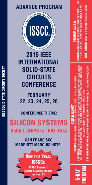
IEEE SOLID-STATE CIRCUITS SOCIETYADVANCE PROGRAM2015 IEEEINTERNATIONALSOLID-STATECIRCUITSCONFERENCEFEBRUARY22, 23, 24, 25, 26CONFERENCE THEME:SILICON SYSTEMSSMALL CHIPS FOR BIG DATASAN FRANCISCOMARRIOTT MARQUIS HOTELNEW THIS YEAR:ISSCCXISSCC PREVIEWS:CIRCUIT & SYSTEM INSIGHTSSEE PAGE: 61THURSDAY ALL-DAY4 FORUMS: ADVANCES IN WIRELESS POWER; LOW POWER FORIOE; RF TRANSMITTER ADVANCES; IO @ 25GB/S & MORESUNDAY ALL-DAY2 FORUMS: HIGH-SPEED INTERLEAVED ADCs; MEMORY TRENDS: BIG DATA TO WEARABLE10 TUTORIALS: RF RECEIVERS; DRAM INTERFACES; ULTRA-LOW-POWER WIRELESS; NEAR-THRESHOLD DESIGN;HIGH-SPEED CURRENT-STEERING DACs; CLOCK & DATA RECOVERY; MANY-CORE PROCESSORS; NANO-POWERANALOG; FREQUENCY SYNTHESIZERS; 3D IMAGING ICsSHORT-COURSE: CMOS LOW-VOLTAGE CIRCUIT DESIGN2 EVENING EVENTS ON GRADUATE STUDENT RESEARCH IN PROGRESS, ICs TALKING TO NEURONS5-DAYPROGRAM
ISSCC VISION STATEMENTThe International Solid-State Circuits Conference is the foremost global forum for presentationof advances in solid-state circuits and systems-on-a-chip. The Conference offers a uniqueopportunity for engineers working at thecutting edge of IC design and application to maintaintechnical currency, and to network with leading experts.CONFERENCE TECHNICAL HIGHLIGHTSOn Sunday, February 22 nd , the day before the official opening of the Conference, ISSCC 2015offers:• A choice of up to 4 of a total of 10 Tutorials• A choice of 1 of 2 all-day Advanced-Circuit-Design ForumsThe 90-minute tutorials offer background information and a review of the basics in specificcircuit-design topics. In the all-day Advanced-Circuit-Design Forums, leading experts presentstate-of-the-art design strategies in a workshop-like format. The Forums are targeted atdesigners experienced in the technical field.On Sunday evening, there are two events: A Special-Topic Session entitled, “Brain-MachineInterfaces: ICs Talking to Neurons” will be offered starting at 8:00pm. In addition, theStudent Research Preview, featuring short presentations followed by a poster session fromselected graduate-student researchers from around the world will begin at 7:30 pm.Introductory remarks at the Preview will be provided by a distinguished member of thesolid-state circuit community.On Monday, February 23 rd , ISSCC 2015 offers three plenary papers on the theme: “SiliconSystems - Small Chips for Big Data”. On Monday at 12:15 pm, there will be a Women’s NetworkingEvent, a luncheon. On Monday afternoon, there will be five parallel technicalsessions, followed by a Social Hour open to all ISSCC attendees. The Social Hour, held inconjunction with the Book Display and Author Interviews, will also include a DemonstrationSession, featuring posters and live demonstrations for selected papers from industry andacademia. Monday evening will include 2 panel sessions on “Moore’s Law Challenges Below10nm…” and “Lost Art? Neat Circuit Tricks with Fewer than a Dozen Transistors”.On Tuesday, February 24 th , there are five parallel technical sessions, both morning andafternoon. A Social Hour open to all ISSCC attendees will follow. The Social Hour, held inconjunction with the Book Display and Author Interviews, will also include a secondDemonstration Session. Tuesday evening sessions include both a panel on “Innovating onthe Tapeout Treadmill”, as well as a Special-Topic Session on “How to Achieve 1000× MoreWireless-Data Capacity. 5G?”.On Wednesday, February 25 th , there will be five parallel technical sessions, both morningand afternoon, followed by Author Interviews.On Thursday, February 26 th , ISSCC offers a choice of five all-day events:• A Short Course on “Circuit Design in Advanced CMOS Techniques:How to Design with Lower Supply Voltages”• Four Advanced-Circuit-Design Forums on“Cutting the Last Wire - Advances in Wireless Power”;“Building the Internet of Everything (IoE):Low-Power Techniques at the Circuit & Systems Level”;“Advanced RF CMOS Transmitter Techniques ”;“IO Design at 25Gb/s & Beyond”.Registration for educational events on Sunday and Thursday will be filled on a first-comefirst-served basis. Use of the ISSCC Web-Registration Site (http://www.isscc.org) is stronglyencouraged. Registrants will be provided with immediate confirmation on registration for theConference, Tutorials, Advanced-Circuit-Design Forums, and the Short Course.Need Additional Information?2Go to: www.isscc.org
TABLE OF CONTENTSTutorials .........................................................................................4-7FORUMSF1 High-Speed Interleaved ADCs ..............................................................................8F2 Memory Trends: From Big Data to Wearable Devices ..........................................9EVENING SESSIONSES1 Student Research Preview .................................................................................10ES2 Brain-Machine Interfaces:Integrated Circuits Talking to Neurons ...............................................................11PAPER SESSIONS1 Plenary Session............................................................................................12-132 RF TX/RX Design Techniques.............................................................................143 Ultra-High-Speed Wireline Transceivers and Energy-Efficient Links ..................154 Processors.........................................................................................................165 Analog Techniques.............................................................................................176 Image Sensors and Displays..............................................................................18Demonstration Session.................................................................................................19EP1EP2EVENING SESSIONSMoore’s Law Challenges Below 10nm:Technology, Design and Economic Implications.................................................20Lost Art? Analog Tricks and Techniques from the Masters.................................20PAPER SESSIONS7 Non-Volatile Memory Solutions .........................................................................218 Low-Power Digital Techniques...........................................................................229 High-Performance Wireless...............................................................................2310 Advanced Wireline Techniques and PLLs...........................................................2411 Sensors and Imagers for Life Sciences..............................................................2512 Inductor-Based Power Conversion.....................................................................2613 Energy-Efficient RF Systems..............................................................................2714 Digital PLLs and SoC Building Blocks................................................................2815 Data-Converter Techniques ................................................................................2916 Emerging Technologies Enabling Next-Generation Systems...............................30Demonstration Session.................................................................................................31Conference Timetable .............................................................................................32-33EVENING SESSIONSEP3 Innovating on the Tapeout Treadmill ..................................................................34ES3 How to Achieve 1000× more Wireless Data Capacity? 5G? ...............................34PAPER SESSIONS17 Embedded Memory and DRAM I/O....................................................................3518 SoCs for Mobile Vision, Sensing and Communications .....................................3619 Advanced Wireless Techniques..........................................................................3720 Energy Harvesting and SC Power Conversion....................................................3821 Innovative Personalized Biomedical Systems ....................................................3922 High-Speed Optical Links...................................................................................4023 Low-Power SoCs ...............................................................................................4124 Secure, Efficient Circuits for IoT ........................................................................4225 RF Frequency Generation from GHz to THz........................................................4326 Nyquist-Rate Converters....................................................................................4427 Physical Sensors ...............................................................................................45SHORT COURSECircuit Design in Advanced CMOS Technologies:How to Design with Lower Supply Voltages .................................................46-48FORUMSF3 Cutting the Last Wire – Advances in Wireless Power.........................................49F4 Building the Internet of Everything (IoE):Low-Power Techniques at the Circuit and System Levels ..................................50F5 Advanced RF CMOS Transmitter Techniques .....................................................51F6 I/O Design at 25Gb/s and Beyond:Enabling the Future Communication Infrastructure for Big Data........................52Committees..............................................................................................................53-57Conference Information...........................................................................................58-61Conference Space Layout .............................................................................................623
TUTORIALSSunday February 22 ndT1: Fundamentals of Modern RF ReceiversTo be compliant with multi-standard applications, the RF front-end of a modern transceivermust satisfy several challenging tasks such as large operative bandwidth, low noise, and highlinearity. Over the years, addressing such requirements has significantly changed the radioarchitecture towards an ultimate solution based on current signal processing and passivemixers. In this tutorial, after a brief description of the typical structure of a receiver, the mainproperties that the radio must satisfy will be defined. After that, voltage and current signalprocessing will be compared showing why a fully current-mode approach is more suitable indeep-scale technologies. The tutorial will end by describing the most popular RF front-endarchitectures with a particular emphasis on the noise-canceling technique and the Class-ABsolutions.Instructor: Antonio LiscidiniAntonio Liscidini received the Laurea degree and Ph.D. in Electrical Engineering from theUniversity of Pavia, Pavia, Italy, in 2002 and 2006 respectively. He was a summer intern atNational Semiconductor in 2003 (Santa Clara, CA) studying polyphase filters and CMOS LNAs.From 2008 to 2012 he was Assistant Professor at the University of Pavia and consultant forMarvell Semiconductor in the area of integrated circuit design. In December 2012 he joinedthe Edward S. Rogers Sr. Department of Electrical & Computer Engineering of the Universityof Toronto. His research interests are in the implementations of transceivers and frequencysynthesizers for cellular and ultra-low-power applications.T2: Basics of DRAM InterfacesMemories have evolved continuously since the simple days of SDRAM. Back then, oneinterface standard was dominating and could be adapted to the different system needs. Now,one size no longer fits all. The number of DRAM standards is proliferating since differentsystem environments require different, tailored DRAM-solutions. Examples are DDRn,GDDR5, HBM, LPDDRn, and WIOn. In this tutorial, we give an overview of these interfacestandards highlighting important details of the specifications, and describe selected designaspects and their system level implications.Instructor: Martin BroxMartin Brox received Dipl. and Dr. degrees from the University of Münster in 1988 and 1992.In 1988 he joined Siemens Corporate Research for a project to improve the modeling ofhot-carrier degradation on CMOS-circuits. In 1992, he moved to the IBM/Siemens/ToshibaDRAM development alliance initially focusing on design, layout and test of DRAM mini-arraysand later DRAM-design. In 1997, he joined Siemens Semiconductor which later becameInfineon and Qimonda where he was responsible for multiple commodity, RDRAM, GDDR3and GDDR5 designs. In 2009 he joined Elpida (now part of Micron) as the lead designengineer for Micron’s GDDR5 development.T3: Ultra-Low-Power Wireless SystemsEmerging applications such as wearable devices, sensor networks and the ‘internet of things’have to operate from very limited power budgets, and thus ultra-low-power operation isbecoming increasingly important. This tutorial will address a range of issues that need to beconsidered in the design of ultra-low-power wireless systems. The tutorial will describe keyfeatures of low-power wireless standards such as BTSmart. We will then give an overviewof architectures appropriate for very low power implementation including superregenerativereceivers, BAW-based architectures and direct modulation transmitters, and willoutline the system trade-offs, which need to be considered for specific applications. We willthen consider some key circuit building blocks required in the receiver, transmitter, andperipheral units and outline design techniques that are suitable for very low powerimplementation.4
TUTORIALSSunday February 22 ndInstructor: Alison BurdettAlison Burdett has over 25 years of experience in semiconductor design. She joined Toumazin 2001 as Technical Director, and is currently responsible for delivering silicon and healthcaretechnology programs within the company. Prior to joining Toumaz, Alison spent time bothin industry as an integrated circuit designer, and also in academia (as Senior Lecturer inAnalogue IC Design at Imperial College London) Dr. Burdett is a Chartered Engineer, a Fellowof the Institute of Engineering and Technology (FIET) and a Senior Member of the IEEE. Sheis European Regional Chair of the Technical Program Committee for the IEEE InternationalSolid State Circuits Conference (ISSCC), a member of the National Microelectronics Institute(NMI) Microelectronics Design Advisory Board, and a Visiting Researcher at the Institute ofBiomedical Engineering, Imperial College.T4: Low-Power Near-threshold DesignDigital circuit energy efficiencies plateaued due to stagnated voltage scaling in sub-90nmtechnologies. As a result, there is renewed interest in operating circuits at low supplyvoltages, such as near the device threshold voltage (referred to as near-threshold or NTdesign). NT operation offers a good balance between performance and energy efficiency, incontrast to sub-threshold design, which sacrifices performance for energy optimality. Thistutorial offers design guidelines for near-threshold operation, particularly related to NT designrobustness. Design examples from both academia and industry will highlight DSPaccelerators, embedded memories, wide-range voltage scalable designs, and variabilitycompensation strategies that scale to NT voltages.Instructor: Dennis SylvesterDennis Sylvester received a Ph.D. from the University of California, Berkeley and is Professorof Electrical Engineering and Computer Science at the University of Michigan, Ann Arbor, MI.He has published over 375 articles along with one book and several book chapters, and holds20 US patents. His research interests include the design of millimeter-scale computingsystems and energy-efficient near-threshold computing. He is co-founder of Ambiq Micro,a fabless semiconductor company developing ultra-low-power mixed-signal solutions forcompact wireless devices. He is an IEEE Fellow.T5: High-Speed Current-Steering DACsAmong the various existing digital-to-analog converter (DAC) architectures, the currentsteeringDAC architecture prevails at high sampling rates. Its simple underlying topologymakes these DACs well-suited for implementation in deep-submicron CMOS processes, wherehigh-speed switches are readily available. The topological simplicity, however, comes with asubstantial sensitivity to many sources of distortion. This tutorial first summarizes the basicsof the current-steering architecture. Subsequently, it covers the various distortionmechanisms as well as the design techniques available to overcome their detrimental effectson DAC performance. Finally, measurement techniques required to assess the performanceof the eventual DAC design are treated.Instructor: Jan MulderJan Mulder received the M.Sc. and Ph.D. degrees in electrical engineering from DelftUniversity of Technology, The Netherlands, in 1994 and 1998, respectively. From 1998 to2000, he was with Philips Research Laboratories, Eindhoven, The Netherlands. In 2000, hejoined Broadcom, Bunnik, The Netherlands, where he has been involved in analog and mixedsignalIC design. He has published over 60 papers and holds more than 35 U.S. patents incircuit design. He served as an Associate Editor for IEEE Trans. on CAS-1 and is a memberof the ISSCC ITPC.5
TUTORIALSSunday February 22 ndT6: Clock and Data Recovery Architectures and CircuitsThis tutorial provides ground theory and practical strategies for the design of clock-anddata-recoverycircuits. We begin by relating performance metrics such as jitter transfer, jittertolerance, and jitter peaking to CDR loop components and use these relationships to elucidateapplication-specific design challenges and tradeoffs. Following this, we will discuss botharchitectural- and circuit-level techniques to manage/overcome these tradeoffs. Specifically,we would compare different architectures: bang-bang vs. linear, digital vs. analog vs. hybridloops, oscillator vs. phase interpolator, and reference-less vs. reference-based CDRs. We thenpresent frequency-locking techniques and conclude with a case study of a recently reportedCDR.Instructor: Pavan Kumar HanumoluPavan Kumar Hanumolu is an Associate Professor in the Department of Electrical andComputer Engineering at the University of Illinois, Urbana-Champaign. He received the Ph.D.degree from the School of Electrical Engineering and Computer Science at Oregon StateUniversity, Corvallis, in 2006, where he subsequently served as a faculty member until 2013.Dr. Hanumolu’s research interests are in energy-efficient integrated circuit implementation ofanalog and digital signal processing, wireline communication systems, and power conversion.He currently serves as an Associate Editor of the Journal of Solid-State Circuits, and is atechnical program committee member of the VLSI Circuits Symposium, and InternationalSolid-State Circuits ConferenceT7: Basics of Many-Core ProcessorsThis tutorial focuses on the design of many-core processors spanning clients to servers tohigh-performance computing systems in scaled CMOS process. Key circuits and designtechniques are highlighted for robust and variation-tolerant logic, embedded memory arraysand on-die interconnect fabrics. Also presented are design principles that enable a widedynamic voltage-frequency operating range, spanning multi-threaded high-throughputnear-threshold voltage to single-threaded burst performance modes. Fine-grain multi-voltagedesign and power management techniques are covered, along with smart variation-awareworkload mapping schemes to achieve maximum performance under stringent thermal andenergy constraints. Real chip design examples are used to illustrate basic design principlesand practical considerations.Instructor: Vivek DeVivek De is an Intel Fellow and Director of Circuit Technology Research in Intel Labs. He isresponsible for providing strategic technical directions for long-term research in future circuittechnologies and leading energy efficiency research across the hardware stack. He has 223publications in refereed international conferences and journals and 195 patents, with 30 morepatents filed (pending). He received an Intel Achievement Award for contributions to integratedvoltage regulator technology. He received a Best Paper Award at the 1996 IEEE InternationalASIC Conference, and nominations for Best Paper Awards at the 2007 IEEE/ACM DesignAutomation Conference (DAC) and the 2008 IEEE/ACM International Conference onComputer-Aided Design (ICCAD). One of his publications was recognized in the 2013IEEE/ACM Design Automation Conference (DAC) as one of the “Top 10 Cited Papers in 50Years of DAC”. He received a Ph.D. in Electrical Engineering from Rensselaer PolytechnicInstitute, Troy, New York. He is a Fellow of the IEEE.T8: Analog Techniques for Nano-power CircuitsThis tutorial presents the design methodology and examples of analog circuits havingnanoampere consumption with application in systems with short activity periods followedlong standby. They are essential for the area of energy harvesting where the amount ofavailable energy can unpredictably change by orders of magnitude. Low load efficiency ofpower management becomes a very important parameter in a wide breadth of applications.Circuit examples include biasing, precision voltage references, oscillators, charge pumps,adaptive speed amplifiers and comparators, LDOs, DCDC converters.6
TUTORIALSSunday February 22 ndInstructor: Vadim IvanovVadim Ivanov received the MSEE and the Ph.D. in 1980 and 1987, respectively, both in theUSSR. He designed electronic systems and ASICs for naval navigation equipment from 1980to 1991 in St. Petersburg, Russia, and mixed-signal ASICs for sensors, GPS/GLONASSreceivers and for motor control between 1991 and 1995. He joined Burr Brown (presentlyTexas Instruments, Tucson) in 1996 as a senior member of technical staff, where he has beeninvolved in the design of the operational, instrumentation, power amplifiers, references, andswitching and linear voltage regulators. He has over 80 US patents and applications on analogcircuit techniques and authored over 30 technical papers and three books: “Power IntegratedAmplifiers” (Leningrad, Rumb, 1987), “Analog system design using ASICs” (Leningrad,Rumb, 1988), both in Russian, and “ Operational Amplifier Speed and AccuracyImprovement”, Kluwer, 2004.T9: Frequency Synthesizers for Wireless TransceiversA frequency synthesizer is a key building block in wireless systems. The DS fractional-N PLLbasedsynthesizer plays a critical role in modern transceivers not only as a local oscillatorbut also as a phase modulator with direct digital modulation. However, the traditional PLL inadvanced CMOS technology suffers from poor scalability, loop parameter variability, leakagecurrent and linearity problems. Accordingly, diversified PLL architectures and circuittechniques have been recently proposed in consideration of performance, power and cost,thus making it more difficult than ever for circuit designers to choose the right design solution.This tutorial gives some insight into PLL basics tailored for circuit designers. Then, systemperspectives and practical circuit design aspects for frequency synthesis will be presented.Instructor: Woogeun RheeWoogeun Rhee is a Professor at Tsinghua University, China. He received the B.S. degree fromSeoul National University in 1991, the M.S. degree from UCLA in 1993, and the Ph.D. degreefrom the University of Illinois, Urbana-Champaign, in 2001. From 1997 to 2001, he was withConexant Systems, CA, where he was a Principal Engineer and developed low-powerlow-cost fractional-N synthesizers. From 2001 to 2006, he was with IBM Thomas J. WatsonResearch Center, NY and worked on clocking area for high-speed I/O serial links. In August2006, he joined the faculty of Tsinghua University, China. He currently holds 19 U.S. patents.T10: CMOS Sensors for 3D Imaging3D imaging has become a hot research topic in the last few years, driven by the needs ofemerging markets looking for next-generation user interfaces based on gesture control.Moreover, 3D vision systems offer amazing possibilities of improvement in many other areaslike automotive, security and surveillance, cultural heritage preservation, ambient-assistedliving, industrial control, etc., because they significantly increase the robustness of objectclassification with respect to conventional 2D imagers. This tutorial will introduce participantsto the exciting field of 3D imaging, providing an overview about image-sensor architecturescapable of distance measurement. An introduction to existing 3D imaging technologies willbe given, addressing the peculiarities of each measuring technique and the possibleapplication domains. The focus is on solid-state sensor architectures as enabling technologiesto improve the performance of 3D vision systems, with a particular emphasis on time-offlightimplementations. Finally, participants will get some practical tools such as figure ofmerits and experimental characterizations guidelines for a comprehensive comparison of 3Dimager performance and a perspective toward the future challenges in this fast-evolving field.Instructor: David StoppaDavid Stoppa received the Ph.D. degree in Microelectronics from the University of Trento,Italy. In 2010 he became head of the Smart Optical Sensors and Interfaces research unit atFBK, where he has been working as a research scientist since 2002. His research interestsare in the field of CMOS image sensors and biosensors. He has published more than 100papers, and holds several patents in the field of image sensors. He is currently a member ofthe ISSCC ITPC and was technical committee member of ‘International Image SensorsWorkshop’ in 2009 and 2013. Dr. Stoppa received the 2006 ESSCIRC Best Paper Award.7
FORUM 1Organizer:Co-organizer:Committee:Sunday February 22 nd , 8:00 AMF1: High-Speed Interleaved ADCsStéphane Le Tual, STmicroelectronics, Crolles, FranceBorivoje Nikolic, University of California, Berkeley, CATetsuya Iizuka, University of Tokyo, Tokyo, JapanIchiro Fujimori, Broadcom, Irvine, CATime-interleaved ADCs have become critical components in high-speed wireline and wirelesscommunication systems. This forum will deliver a comprehensive treatment of state-of-theart design techniques for high-speed interleaved ADCs. Topics include transistor-level designtechniques, calibration (estimation & correction), as well as the link between systemspecifications and required ADC performance.TimeTopic8:00 AM BreakfastAgenda8:20 AM Introduction by Chair8:30 AM Interleaved ADCs Through the AgesKen Poulton, Keysight Laboratories, Santa Clara, CA9:20 AM Mismatch Error Correction for High-Resolution,GS/s time-Interleaved ADCsPer Löwenborg, Signal Processing Devices, Linköping, Sweden10:10 AM Break10:35 AM Highly Accurate Adaptive Digital Calibration for High-SpeedHigh-Resolution Time-Interleaved ADCsTakashi Oshima, Hitachi, Tokyo, Japan11:25 AM ADC Interleaving Errors Corrected by Adaptive Post-ProcessingAsad Abidi, University of California, Los Angeles, CA12:15 PM Lunch1:20 PM Specifications vs. Applications: Driving Architectural ChoicesAaron Buchwald, Entropic, Irvine, CA2:10 PM GS/s Time-Interleaved ADCs for Broadband Multi-CarrierSignal ReceptionKostas Doris, NXP, Eindhoven, The Netherlands3:00 PM Break3:20 PM Embedded CMOS ADCs for Optical CommunicationsYuriy M. Greshishchev, Ciena, Ottawa, Canada4:10 PM PanelModerators: Bora Nikolic (UC Berkeley)Dave Robertson (ADI)5:00 PM Closing remarks by Chair8
FORUM 2Sunday February 22 nd , 8:00 AMF2: Memory Trends: From Big Data to Wearable DevicesOrganizer:Committee:Jonathan Chang, TSMC, Hsinchu, TaiwanJonathan Chang, TSMC, Hsinchu, TaiwanLeland Chang, IBM, Yorktown Heights, NYAntoine Dupret, CEA Leti-LIST, Gif-sur-Yvette, FranceChulwoo Kim, Korea University, Seoul, KoreaFatih Hamzaoglu, Intel, Hillsboro, ORTakefumi Yoshikawa, Panasonic, Kyoto, JapanMemory continues to be a critical element in the full range of VLSI applications - from bigdata to mobile applications to wearable devices. Recent trends, including process technologyscaling limits, new memory applications, and evolving high-performance and low-powerrequirements, have driven the development of emerging memories. As both discrete andembedded memory scaling becomes ever more challenging, there is a widespread effort tolook for alternative memory technologies to replace the entrenched SRAM, DRAM, or Flash.This forum will bring together systems designers to discuss memory needs for futureapplications and memory designers to describe the latest developments in emerging and nextgeneration memories.AgendaTimeTopic8:00 AM Breakfast8:20 AM Introduction8:30 AM Memory Requirement Trends and Challenges: Servers to DevicesSuresh Chittor, Intel, Hillsboro, OR9:20 AM Memory System Requirements for the Big-Data ApplicationData-Centric ComputingKen Takeuchi, Chuo University, Tokyo, Japan10:10 AM Break10:35 AM Memory and Storage Requirement and Trend for ChromeOSEric Shiu, Google, Mountain View, CA11:25 AM Emerging Memories in Embedded Systems: Opportunities for theDigital Architect, Challenges for the DesignersFabien Clermidy, CEA-Leti, Grenoble, France12:15 PM Lunch1:20 PM 3D NAND Flash: from Enterprise to Embedded StoragesKi-Tae Park, Samsung, Hwasung, Korea2:10 PM Addressing Future Memory Challenges with Device AbstractionJ. Thomas Pawlowski, Micron, Boise, ID3:00 PM Break3:20 PM Technology Trends and Applications of MRAMfrom Big Data to Wearable DevicesShinobu Fujita, Toshiba, Kawasaki, Japan4:10 PM RRAM for Data Abundant System Technology:Managing Expectations and Minimizing DisappointmentsMalgorzata Jurczak, IMEC, Leuven, Belgium5:00 PM Conclusion9
EVENING SESSIONSunday February 22 nd , 7:30 PMES1: STUDENT RESEARCH PREVIEW (SRP)The Student Research Preview (SRP) will highlight selected student research projectsin progress. The SRP consists of 25 one-minute presentations followed by a PosterSession, by graduate students from around the world, which have been selected on thebasis of a short submission concerning their on-going research. Selection is based onthe technical quality and innovation of the work. This year, the SRP will be presented inthree theme sections: Low-Power Data Converters and High-Speed Links; BiomedicalCircuits and Systems; and Energy-Efficient Circuits for Sensors, RF, and Platform.The Student Research Preview will begin with a brief talk by a distinguished member ofthe solid-state circuit community, Professor Emerita Lynn Conway of the University ofMichigan, Ann Arbor.Her remarks are scheduled for Sunday, February 22 nd , starting at 7:30 pm. SRP is opento all ISSCC registrants.Chair: Jan Van der Spiegel University of Pennsylvania, USACo-Chair: SeongHwan Cho KAIST, KoreaCo-Chair: Marian Verhelst Kath. University of Leuven, BelgiumSecretary: SeongHwan Cho KAIST, KoreaAdvisor: Kenneth C. Smith University of Toronto, CanadaMedia/Publications: Laura Fujino University of Toronto, CanadaA/V: John Trnka Rochester, MNCOMMITTEE MEMBERSBryan Ackland, Stevens Institute of Technology, USAAndrea Baschirotto, University of Milan-Bicocca, ItalyWilliam Bowhill, Intel, USASeongHwan Cho, KAIST, KoreaDenis Daly, Maxim Integrated, USAAndreas Demosthenous, University College London, UKVincent Gaudet, University of Waterloo, CanadaManish Goel, Samsung Electronics, USAChun-Huat Heng, National University of Singapore, SingaporeMakoto Ikeda, University of Tokyo, JapanJaeha Kim, Seoul National University, KoreaTsung-Hsien Lin, National Taiwan University, TaiwanDejan Marković, University of California, Los Angeles, USAAkira Matsuzawa, Tokyo Institute of Technology, JapanShahriar Mirabbasi, University of British Columbia, CanadaTinoosh Mohsenin, University of Maryland, USANils Pohl, Ruhr-University Bochum, GermanyPatrick Reynaert, University of Leuven, BelgiumBing Sheu, TSMC, TaiwanSameer Sonkusale, Tufts University, USAJan Van der Spiegel, University of Pennsylvania, USAMarian Verhelst, University of Leuven, BelgiumJeffrey Weldon, Carnegie Mellon University, USAGuoXing Wang, Shanghai Jiao Tong University, ChinaPeter (Chung-Yu) Wu, National Chiao Tung University, Taiwan10
EVENING SESSIONSunday February 22 nd , 8:00 PMES2: Brain-Machine Interfaces:Integrated Circuits Talking to NeuronsOrganizer:Chair:Firat Yazicioglu, IMEC, Leuven, BelgiumPeng Cong, Google, Mountain View, CAShahriar Mirabbasi, University of British Columbia,Vancouver, CanadaPeng Cong, Google, Mountain View, CAShahriar Mirabbasi, University of British Columbia,Vancouver, CanadaWe have not unlocked the three pounds of matter sitting in between our ears.-Barack ObamaThe brain is the most complex human organ, with energy efficiency far beyond that of anyexisting equivalent computing technology. Great efforts are being invested globally intodeciphering its functioning. If successful, the resulting knowledge may forever changemedical, consumer, and communications semiconductor industry sectors. A first significantchallenge on the road towards this goal is the creation of instruments, generally enabled byintegrated circuits, which can interact with a large number of the brain neurons and interpretsuch interactions.This evening session will discuss technologies and circuit design solutions for connectingintegrated circuits to neural circuits and will explore future application opportunities for suchbrain-machine interfaces. Experts in related technologies, circuit design, and applicationsfrom three continents will present an entertaining session on the impact of semiconductortechnologies on medical applications and human-machine interaction.TimeTopic8:00 PM Neural Interfacing: Challenges and Opportunities for Circuit DesignersTim Denison, Medtronic, Minneapolis, MN8:25 PM CMOS Technology to Interface with Single Neurons and AxonsAndreas Hierlemann, ETHZ, Zurich, Switzerland8:50 PM Circuits and Systems for Implantable Brain MonitoringJan Rabaey, University of California, Berkeley, CA9:15 PM Neural Stimulation and Closed-Loop ProstheticsMinkyu Je, Daegu Gyeongbuk Institute of Science & Technology,Daegu, Korea9:40 PM Panel Discussions11
SESSION 1Plenary Session — Invited PapersChair: Anantha Chandrakasan, Massachusetts Institute of Technology, Cambridge, MAISSCC Conference ChairAssociate Chair: Hoi-Jun Yoo, KAIST, Daejeon, KoreaISSCC Program Committee ChairMonday February 23 rd , 8:30 AMFORMAL OPENING OF THE CONFERENCE8:30 AM1.1 Silicon Technologies and Solutions for the Data-Driven World 8:45 AMKinam Kim, President, Samsung Electronics, Kiheung, KoreaSilicon technology has been the core driver of the modern information revolution, formingthe foundation on which electronics devices have been built. Advances in silicon-scalingtechnology have placed general-purpose computing in the palm of one’s hand! Despiteconcerns for the demise of scaling, higher performance in electronic systems for the comingdecades is expected, thanks to innovations in materials, structures, and processes.Performance-enhancing technologies, such as TSVs and 3D ICs, will drive the evolution ofthe fast-expanding data-driven world. As usual, these technological advances will breed newapplications and new fields (Internet of Things, mobile healthcare, and others), all of whichwill catalyze explosive data growth. Both silicon and silicon-system technologies will need toevolve in order to conform to the future data-driven world. Future system-technologydirections from the perspectives of servers, clients, and connectivity will also be discussed.Finally, issues associated with this data explosion (such as data security) will be presented.ISSCC, SSCS, IEEE AWARD PRESENTATIONS9:25 AMBREAK9:55 AM1.2 The Future of IC Design Innovation 10:10 AMSehat Sutardja, Chairman and CEO, Marvell Technology Group,Santa Clara, CAOne of the greatest achievements of humankind is undoubtedly our ability to build tinymachines that marry the functionalities of computers and wireless communication devicesso cheaply that almost anyone in the world can afford them. Every one of us has at least onesuch device in our pocket, yet we rarely think about how in the world anyone could havecreated such a thing! Even the experts in our industry could not have predicted that this wouldhave happened so soon. What we have achieved could be considered nothing short of amiracle, considering that billions of transistors have to work together flawlessly. (Well, sortof.) The reality is that some of these devices are now so complex that we need thousands ofengineers for design, validation, and support, which inevitably causes inefficiencies and bugs.Sadly, the way we build these devices has not changed much over the past decades.Integrated-circuit design engineers blindly do what they are told to – integrate as muchfunctionality into a single device, believing that more is better! This more- the-better mentalityis not surprising because we saw in the past that the more we integrate, the cheaper thingswould become. Unfortunately, times have changed. The cost and complexity of buildingbillions of transistors on a single device is finally taking a toll on our engineers. If chip-designengineers had also looked at the financial optimization of the overall design process, theywould have built things differently. They should have realized that certain functions are bettergrouped into highly specialized integrated circuits that could easily and seamlessly talk toeach other without compromising the overall system cost. The key to making this happen iswhat I call the Lego-Block approach of designing integrated circuits. However, in order forthe Lego-Block approach to materialize, we need to change the way we architect our devices.12
SESSION 1Monday February 23 rd , 10:50 AMWe need to do many things: Define a new chip-to-chip interconnect protocol; take advantageof multi-chip-module packaging and high-speed SerDes technology; redefine the memoryhierarchy to take advantage of 3D solid-state memory instead of blindly increasing the DRAMsize in our devices; repartition DRAM to serve different logical functions instead of buildinggigantic single-die DRAM to serve every function; change the way we build DRAMs so thatthey are optimized more for performance and power efficiency instead of capacity; andredefine what should be done in hardware versus software. In short, we need to change ourway of thinking, and be brave enough to reject common wisdom. If we fail to take action,soon we will no longer see cost savings. On the other hand, if we succeed, we will see lifebeyond the end of Moore’s Law!1.3 Analog CMOS from 5 Micrometer to 5 Nanometer 10:50 AMWilly Sansen, Professor Emeritus, Katholieke Universiteit Leuven,Leuven, BelgiumSince the early years of analog design in CMOS, expertise has been focused on buildingblocks, with emphasis on trade-offs among speed, noise, and power consumption. However,present application systems (such as mobile SoC, Internet of Things, automotive, biomedical,FPGA interfaces), all require mixed-signal design and digitally assisted analog design. “Howmuch analog has to be combined with how much digital?” is an open question.This presentation will briefly look at the history of CMOS analog design and predict howanalog may look in future nanometer CMOS. In these new technologies, the supply voltagekeeps on shrinking, making the effects of offset and 1/f noise even more important thanbefore.Nowadays, analog techniques all aim at the cancellation of resistances, to save power. Theyalso try to cancel capacitances, to enhance speed. As well, cancellation of noise and distortionhave become commonplace. Such cancellation techniques will be reviewed and compared.In parallel, several technologies such as FinFETs and FD-SOI, are in competition for futurenanometer design. Below gate lengths of 10nm, materials other than silicon, such asgermanium, need to be considered. Also, nanowires and nanotubes have become viablecandidates for nanometer analog.PRESENTATION TO PLENARy SPEAKERS11:30 AMCONCLUSION11:35 AM13
SESSION 2Session Chair:Associate Chair:Monday February 23 rd , 1:30 PMRF TX/RX Design TechniquesEhsan Afshari, Cornell University, Ithaca, NYMinoru Fujishima, Hiroshima University, Hiroshima, Japan2.1 A Highly Linear Inductorless Wideband Receiver with Phase- 1:30 PMand Thermal-Noise CancellationH. Wu 1,2 , M. Mikhemar 2 , D. Murphy 2 , H. Darabi 2 , M-C. F. Chang 11University of California, Los Angeles, CA; 2 Broadcom, Irvine, CA2.2 A +70dBm IIP3 Single-Ended Electrical-Balance Duplexer 2:00 PMin 0.18µm SOI CMOSB. van Liempd 1 , B. Hershberg 1 , K. Raczkowski 1 , S. Ariumi 2 ,U. Karthaus 3 , K-F. Bink 3 , J. Craninckx 11imec, Leuven, Belgium; 2 Murata, Kyoto, Japan3HiSilicon, Leuven, Belgium2.3 A 130-to-180GHz 0.0035mm 2 SPDT Switch with 3.3dB Loss and 2:15 PM23.7dB Isolation in 65nm Bulk CMOSF. Meng 1 , K. Ma 1 , K. S. Yeo 1,21Nanyang Technological University, Singapore, Singapore2Singapore University of Technology and Design, Singapore, Singapore2.4 A 0.028mm 2 11mW Single-Mixing Blocker-Tolerant Receiver 2:30 PMwith Double-RF N-Path Filtering, S 11 Centering, +13dBm OB-IIP3and 1.5-to-2.9dB NFZ. Lin 1 , P-I. Mak 1 , R. P. Martins 1,21University of Macau, Macau, China2Instituto Superior Tecnico, Lisbon, Portugal2.5 A 2-to-6GHz Class-AB Power Amplifier with 28.4% PAE in 65nm 2:45 PMCMOS Supporting 256QAMW. Ye 1 , K. Ma 1 , K. S. Yeo 1,21Nanyang Technological University, Singapore, Singapore2Singapore University of Technology and Design, Singapore, SingaporeBreak3:00 PM2.6 Class-O: A Highly Linear Class of Power Amplifiers in 0.13μm 3:15 PMCMOS for WCDMA/LTE ApplicationsA. F. Aref, R. Negra, M. Abdullah KhanRWTH Aachen University, Aachen, Germany2.7 A Hybrid Supply Modulator with 10dB ET Operation Dynamic 3:45 PMRange Achieving a PAE of 42.6% at 27.0dBm PA Output PowerS-C. Lee, J-S. Paek, J-H. Jung, Y-S. Youn, S-J. Lee, M-S. Cho, J-J. Han,J-H. Choi, Y-W. Joo, T. Nomiyama, S-H. Lee, I-Y. Sohn, T. B. Cho,B-H. Park, I. KangSamsung Electronics, Hwaseong, Korea2.8 A Broadband CMOS Digital Power Amplifier with Hybrid 4:15 PMClass-G Doherty Efficiency EnhancementS. Hu 1 , S. Kousai 2 , H. Wang 11Georgia Institute of Technology, Atlanta, GA; 2 Toshiba, Kawasaki, Japan2.9 A 29dBm 18.5% Peak PAE mm-Wave Digital Power Amplifier 4:45 PMwith Dynamic Load ModulationK. Datta, H. Hashemi, University of Southern California, Los Angeles, CA2.10 A 60GHz 28nm UTBB FD-SOI CMOS Reconfigurable Power 5:00 PMAmplifier with 21% PAE, 18.2dBm P 1dB and 74mW P DCA. Larie 1,2 , E. Kerhervé 2 , B. Martineau 1,3 , L. Vogt 1 , D. Belot 1,31STMicroelectronics, Crolles, France2University of Bordeaux, Talence, France3CEA-LETI-MINATEC, Grenoble, FranceConclusion5:15 PM14
SESSION 3Monday February 23 rd , 1:30 PMUltra-High-Speed Wireline Transceiversand Energy-Efficient LinksSession Chair: Ken Chang, Xilinx, San Jose, CAAssociate Chair: Shunichi Kaeriyama, Renesas, Tokyo, Japan3.1 A 28Gb/s Multi-Standard Serial-Link Transceiver 1:30 PMfor Backplane Applications in 28nm CMOSB. Zhang, K. Khanoyan, H. Hatamkhani, H. Tong, K. Hu,S. Fallahi , K. Vakilian, A. BrewsterBroadcom, Irvine, CA3.2 Multi-Standard 185fs rms 0.3-to-28Gb/s 40dB Backplane 2:00 PMSignal Conditioner with Adaptive Pattern-Match 36-TapDFE and Data-Rate-Adjustment PLL in 28nm CMOST. Kawamoto 1 , T. Norimatsu 1 , K. Kogo 1 , F. Yuki 1 , N. Nakajima 2 ,M. Tsuge 2 , T. Usugi 2 , T. Hokari 2 , H. Koba 2 , T. Komori 2 , J. Nasu 2 ,T. Kawamata 2 , Y. Ito 2 , S. Umai 2 , J. Kumazawa 2 , H. Kurahashi 2 ,T. Muto 2 , T. Yamashita 2 , M. Hasegawa 2 , K. Higeta 21Hitachi, Tokyo, Japan2Hitachi, Kanagawa, Japan3.3 A 0.5-to-32.75Gb/s Flexible-Reach Wireline 2:30 PMDS Transceiver in 20nm CMOSP. Upadhyaya, J. Savoj, F-T. An, A. Bekele, A. Jose, B. Xu,D. Wu, D. Turker, H. Aslanzadeh, H. Hedayati, J. Im, S-W. Lim,S. Chen, T. Pham, Y. Frans, K. ChangXilinx, San Jose, CABreak3:00 PM3.4 A 36Gb/s PAM4 Transmitter Using an 8b 18GS/s DAC 3:15 PMin 28nm CMOSA. Nazemi, K. Hu, B. Catli, D. Cui, U. Singh, T. He, Z. Huang,B. Zhang, A. Momtaz, J. CaoBroadcom, Irvine, CA3.5 A 16-to-40Gb/s Quarter-Rate NRZ/PAM4 Dual-Mode 3:45 PMTransmitter in 14nm CMOSJ. Kim, A. Balankutty, A. Elshazly, Y-Y. Huang, H. Song,K. Yu, F. O’MahonyIntel, Hillsboro, OR3.6 A 10Gb/s Hybrid ADC-Based Receiver with Embedded 3-Tap Analog 4:00 PMFFE and Dynamically-Enabled Digital Equalization in 65nm CMOSA. Shafik, E. Zhian Tabasy, S. Cai, K. Lee, S. Hoyos, S. PalermoTexas A&M University, College Station, TX3.7 A 7Gb/s Rapid On/Off Embedded-Clock Serial-Link Transceiver 4:15 PMwith 20ns Power-On Time, 740µW Off-State Power forEnergy-Proportional Links in 65nm CMOST. Anand 1 , M. Talegaonkar 1 , A. Elkholy 1 , S. Saxena 1 , A. Elshazly 2 ,P. K. Hanumolu 11University of Illinois, Urbana, IL2Intel, Hillsboro, OR3.8 A 0.45-to-0.7V 1-to-6Gb/s 0.29-to-0.58pJ/b Source-Synchronous 4:45 PMTransceiver Using Automatic Phase Calibration in 65nm CMOSW-S. Choi 1 , G. Shu 1 , M. Talegaonkar 1 , Y. Liu 1 , D. Wei 1 , L. Benini 2 ,P. K. Hanumolu 11University of Illinois, Urbana, IL2University of Bologna, Bologna, ItalyConclusion5:15 PM15
SESSION 4Monday February 23 rd , 1:30 PMProcessorsSession Chair: Atsuki Inoue, Fujitsu, Kawasaki, JapanAssociate Chair: Luke (Jinuk) Shin, Oracle, Redwood Shores, CA4.1 22nm Next-Generation IBM System z Microprocessor 1:30 PMJ. Warnock 1 , B. Curran 2 , J. Badar 3 , G. Fredeman 2 , D. Plass 2 , Y. Chan 2 ,S. Carey 2 , G. Salem 4 , F. Schroeder 5 , F. Malgioglio 2 , G. Mayer 5 , C. Berry 2 ,M. Wood 2 , Y-H. Chan 2 , M. Mayo 2 , J. Isakson 3 , C. Nagarajan 6 , T. Werner 5 ,L. Sigal 7 , R. Nigaglioni 3 , M. Cichanowski 3 , J. Zitz 8 , M. Ziegler 7 , T. Bronson 3 ,G. Strevig 3 , D. Dreps 3 , R. Puri 7 , D. Malone 2 , D. Wendel 5 , P-K. Mak 2 , M. Blake 21IBM Systems and Technology, Yorktown Heights, NY2IBM Systems and Technology, Poughkeepsie, NY3IBM Systems and Technology, Austin, TX4IBM Systems and Technology, Williston, VT5IBM Systems and Technology, Boeblingen, Germany6IBM Systems and Technology, Bangalore, India7IBM Research, Yorktown Heights, NY8IBM Systems and Technology, Hopewell Junction, NY4.2 A 20nm 32-Core 64MB L3 Cache SPARC M7 Processor 2:00 PMP. Li, J. L. Shin, G. Konstadinidis, F. Schumacher, V. Krishnaswamy,H. Cho, S. Dash, R. Masleid, C. Zheng, Y. D. Lin, P. Loewenstein,H. Park, V. Srinivasan, D. Huang, C. Hwang, W. Hsu, C. McAllisterOracle, Redwood Shores, CA4.3 Fine-Grained Adaptive Power Management of the 2:30 PMSPARC M7 ProcessorV. Krishnaswamy, J. Brooks, G. Konstadinidis, C. McAllister,H. Pham, S. Turullols, J. L. Shin, Y. YangGong, H. ZhangOracle, Redwood Shores, CA4.4 Energy-Efficient Microserver Based on a 12-Core 1.8GHz 2:45 PMDS 188K-CoreMark 28nm Bulk CMOS 64b SoC for Big-DataApplications with 159GB/s/L Memory Bandwidth System DensityR. Luijten 1 , D. Pham 2 , R. Clauberg 1 , M. Cossale 1 , H. N. Nguyen 2 , M. Pandya 21IBM Research, Rüschlikon, Switzerland2Freescale Semiconductor, Austin, TXBreak3:00 PM4.5 The Xeon® Processor E5-2600 v3: A 22nm 18-Core Product Family 3:15 PMB. Bowhill 1 , B. Stackhouse 2 , N. Nassif 1 , Z. Yang 1 , A. Raghavan 1 ,C. Morganti 2 , C. Houghton 1 , D. Krueger 2 , O. Franza 1 , J. Desai 2 ,J. Crop 2 , D. Bradley 2 , C. Bostak 2 , S. Bhimji 1 , M. Becker 11Intel, Hudson, MA; 2 Intel, Fort Collins, CO4.6 A 1.93TOPS/W Scalable Deep Learning/Inference Processor 3:45 PMwith Tetra-Parallel MIMD Architecture for Big-Data ApplicationsS. Park, K. Bong, D. Shin, J. Lee, S. Choi, H-J. Yoo, KAIST, Daejeon, Korea4.7 A 409GOPS/W Adaptive and Resilient Domino Register File in 4:15 PM22nm Tri-Gate CMOS Featuring In-Situ Timing Margin and ErrorDetection for Tolerance to Within-Die Variation, Voltage Droop,Temperature and AgingJ. P. Kulkarni, C. Tokunaga, P. Aseron, T. Nguyen Jr, C. Augustine,J. Tschanz, V. DeIntel, Hillsboro, OR4.8 A 28nm x86 APU Optimized for Power and Area Efficiency 4:45 PMDS K. Wilcox 1 , D. Akeson 1 , H. R. Fair III 1 , J. Farrell 1 , D. Johnson 2 ,G. Krishnan 1 , H. McIntyre 3 , E. McLellan 1 , S. Naffziger 2 , R. Schreiber 4 ,S. Sundaram 4 , J. White 11AMD, Boxborough, MA; 2 AMD, Fort Collins, CO3AMD, Sunnyvale, CA; 4 AMD, Austin, TXConclusion5:15 PM16
SESSION 5Monday February 23 rd , 1:30 PMAnalog TechniquesSession Chair: Xicheng Jiang, Broadcom, Irvine, CAAssociate Chair: Ed (Adrianus JM) van Tuijl, University of Twente,Enschede, The Netherlands5.1 A 60V Auto-zero and Chopper Operational Amplifier with 800kHz 1:30 PMInterleaved Clocks and Input Bias-Current TrimmingY. Kusuda, Analog Devices, San Jose, CA5.2 A 110dB SNR ADC with ±30V Input Common-Mode Range and 2:00 PM8µV Offset for Current Sensing ApplicationsL. Xu 1 , B. Gönen 1 , Q. Fan 2 , J. H. Huijsing 1 , K. A. Makinwa 11Delft University of Technology, Delft, The Netherlands2Maxim Integrated Products, Delft, The Netherlands5.3 A 2-Channel -83.2dB Crosstalk 0.061mm 2 CCIA with an 2:30 PMOrthogonal Frequency Chopping TechniqueY-L. Tsai, F-W. Lee, T-Y. Chen, T-H. LinNational Taiwan University, Taipei, Taiwan5.4 A 32nW Bandgap Reference Voltage Operational from 0.5V 2:45 PMSupply for Ultra-Low Power SystemsA. Shrivastava, K. Craig, N. E. Roberts, D. D. Wentzloff, B. H. CalhounPsiKick, Charlottesville, VABreak3:00 PM5.5 A Forward-Body-Bias Tuned 450MHz Gm-C 3 rd -Order Low-Pass Filter 3:15 PMin 28nm UTBB FD-SOI with >1dBVp IIP3 over a 0.7-to-1V SupplyJ. Lechevallier 1,2 , R. Struiksma 1 , H. Sherry 2 , A. Cathelin 2 ,E. Klumperink 1 , B. Nauta 11University of Twente, Enschede, The Netherlands2STMicroelectronics, Crolles, France5.6 A 0.13µm Fully Digital Low-Dropout Regulator with Adaptive 3:45 PMControl and Reduced Dynamic Stability for Ultra-Wide DynamicRangeS. B. Nasir, S. Gangopadhyay, A. RaychowdhuryGeorgia Institute of Technology, Atlanta, GA5.7 A 29nW Bandgap Reference Circuit 4:15 PMJ. M. Lee 1 , Y. Ji 1 , S. Choi 1 , Y-C. Cho 2 , S-J. Jang 2 , J. S. Choi 2 , B. Kim 1 ,H-J. Park 1 , J-Y. Sim 11Pohang University of Science and Technology, Pohang, Korea2Samsung Electronics, Hwaseong, Korea5.8 A Digitally Assisted Single-Point-Calibration CMOS Bandgap 4:30 PMVoltage Reference with a 3σ Inaccuracy of ±0.08% forFuel-Gauge ApplicationsG. Maderbacher, S. Marsili, M. Motz, T. Jackum, J. Thielmann,H. Hassander, H. Gruber, F. Hus, C. SandnerInfineon Technologies, Villach, Austria5.9 A 37µW Dual-Mode Crystal Oscillator for Single-Crystal Radios 4:45 PMD. Griffith 1 , J. Murdock 1 , P. T. Røine 2 , T. Murphy 11Texas Instruments, Dallas, TX; 2 Texas Instruments, Oslo, Norway5.10 A 4.7MHz 53µW Fully Differential CMOS Reference Clock 5:00 PMOscillator with –22dB Worst-Case PSNR for Miniaturized SoCsJ. Lee 1 , P. Park 1 , S. Cho 2 , M. Je 31Institute of Microelectronics, Singapore, Singapore2KAIST, Daejeon, Korea3Daegu Gyeongbuk Institute of Science and Technology, Daegu, KoreaConclusion5:15 PM17
SESSION 6Monday February 23 rd , 1:30 PMImage Sensors and DisplaysSession Chair: Yusuke Oike, Sony, Atsugi, JapanAssociate Chair: Young-Sun Na, LG Electronics, Seoul, Korea6.1 A 1/1.7-inch 20Mpixel Back-Illuminated Stacked CMOS Image 1:30 PMSensor for New Imaging ApplicationsA. Suzuki 1 , N. Shimamura 1 , T. Kainuma 1 , N. Kawazu 1 , C. Okada 1 , T. Oka 1 ,K. Koiso 2 , A. Masagaki 1 , Y. Yagasaki 3 , S. Gonoi 4 , T. Ichikawa 1 , M. Mizuno 5 ,T. Sugioka 1 , T. Morikawa 1 , Y. Inada 1 , H. Wakabayashi 11Sony, Atsugi, Japan2Sony Semiconductor, Kikuyou, Japan3Sony, Shinagawa, Japan4Sony LSI Design, Fukuoka, Japan5Sony LSI Design, Atsugi, Japan6.2 133Mpixel 60fps CMOS Image Sensor with 32-Column Shared 2:00 PMHigh-Speed Column-Parallel SAR ADCsR. Funatsu 1 , S. Huang 2 , T. Yamashita 1 , K. Stevulak 2 , J. Rysinski 2 ,D. Estrada 2 , S. Yan 2 , T. Soeno 1 , T. Nakamura 1 , T. Hayashida 1 ,H. Shimamoto 1 , B. Mansoorian 21NHK Science & Technology Research Laboratories, Tokyo, Japan2Forza Silicon, Pasadena, CA6.3 A 45.5µW 15fps Always-On CMOS Image Sensor for Mobile and 2:30 PMWearable DevicesJ. Choi, J. Shin, D. Kang, D-S. ParkSamsung Advanced Institute of Technology, Suwon, KoreaBreak3:00 PM6.4 Single-Shot 200Mfps 5×3-Aperture Compressive CMOS Imager 3:15 PMF. Mochizuki 1 , K. Kagawa 1 , S-I. Okihara 2 , M-W. Seo 1 , B. Zhang 1 ,T. Takasawa 1 , K. Yasutomi 1 , S. Kawahito 11Shizuoka University, Hamamatsu, Japan2The Graduate School for the Creation of New Photonics Industries,Hamamatsu, Japan6.5 25.3μW at 60fps 240×160-Pixel Vision Sensor for Motion 3:45 PMCapturing with In-Pixel Non-Volatile Analog Memory UsingCrystalline Oxide Semiconductor FETT. Ohmaru 1 , T. Nakagawa 1 , S. Maeda 1 , Y. Okamoto 1 , M. Kozuma 1 ,S. Yoneda 1 , H. Inoue 1 , Y. Kurokawa 1 , T. Ikeda 1 , Y. Ieda 1 , N. Yamade 1 ,H. Miyairi 1 , M. Ikeda 2 , S. Yamazaki 11Semiconductor Energy Laboratory, Kanagawa, Japan2University of Tokyo, Tokyo, Japan6.6 A 240Hz-Reporting-Rate Mutual-Capacitance Touch-Sensing 4:00 PMDS Analog Front-End Enabling Multiple Active/Passive Styluseswith 41dB/32dB SNR for 0.5mm DiameterM. Hamaguchi, M. Takeda, M. MiyamotoSHARP, Tenri, Japan6.7 A 2.3mW 11cm-Range Bootstrapped and Correlated-Double- 4:15 PMSampling (BCDS) 3D Touch Sensor for Mobile DevicesL. Du, Y. Zhang, F. Hsiao, A. Tang, Y. Zhao, Y. Li, Z-Z. Chen,L. Huang, M-C. F. ChangUniversity of California, Los Angeles, CA6.8 A Pen-Pressure-Sensitive Capacitive Touch System Using 4:45 PMElectrically Coupled Resonance PenC. Park 1,2 , S. Park 2 , K-D. Kim 1 , S. Park 1 , J. Park 2 , Y. Huh 1 ,B. Kang 2 , G-H. Cho 11KAIST, Daejeon, Korea2Samsung Electronics, Suwon, KoreaConclusion5:15 PM18
DEMONSTRATION SESSION MONDAy FEBRUARy 23 RD , TUESDAy, FEBRUARy 24 TH 4:00-7:00 PMThis year, the Demonstration Session extending in selected regular papers, both Academic and Industrial,will take place on Monday February 23 rd , and Tuesday February 24 th , from 4 pm until 7 pm in the GoldenGate Hall. These demonstrations will feature real-life applications made possible by new ICs presented atISSCC 2015, as noted by the symbol, DS in the final Advance Program (available at www.isscc.org)along with the scheduling details, shortly before the Conference. Meanwhile, a list of the selected papersis as follows:Monday, February 23rd3.3 A 0.5-to-32.75Gb/s Flexible-Reach Wireline 2:30 PMTransceiver in 20nm CMOS4.4 Energy-Efficient Microserver Based on a 12-Core 1.8GHz 2:45 PM188K-CoreMark 28nm Bulk CMOS 64b SoC for Big-DataApplications with 159GB/s/L Memory Bandwidth System Density4.8 A 28nm x86 APU Optimized for Power and Area Efficiency 4:45 PM6.6 A 240Hz-Reporting-Rate Mutual-Capacitance Touch-Sensing 4:00 PMAnalog Front-End Enabling Multiple Active/Passive Styluseswith 41dB/32dB SNR for 0.5mm DiameterTuesday, February 24th7.7 Enterprise-Grade 6× Fast Read and 5× Highly Reliable SSD 11:45 AMwith TLC NAND-Flash Memory for Big-Data Storage10.1 A 6Gb/s 6pJ/b 5mm-Distance Non-Contact Interface for 8:30 AMModular Smartphones Using Two-Fold Transmission-LineCoupler and EMC-Qualified Pulse Transceiver11.1 A Time-Divided Spread-Spectrum Code Based 15pW-Detectable 8:30 AMMulti-Channel fNIRS IC for Portable Functional Brain Imaging11.3 A 160×120-Pixel Analog-Counting Single-Photon Imager 9:30 AMwith Sub-ns Time-Gating and Self-Referenced Column-ParallelA/D Conversion for Fluorescence Lifetime Imaging11.8 Integrated Ultrasonic System for Measuring 12:00 PMBody-Fat Composition12.6 90% Peak Efficiency Single-Inductor-Multiple-Output DC-DC 4:15 PMBuck Converter with Output Independent Gate Drive Control13.2 A 3.7mW-RX 4.4mW-TX Fully Integrated Bluetooth 2:00 PMLow-Energy/IEEE802.15.4/Proprietary SoC with anADPLL-Based Fast Frequency Offset Compensationin 40nm CMOS13.3 A 10mW Bluetooth Low-Energy Transceiver with On-Chip Matching 2:15 PM13.7 A +10dBm 2.4GHz Transmitter with Sub-400pW Leakage and 4:15 PM43.7% System Efficiency15.8 A 90dB-SFDR 14b 500MS/s BiCMOS Switched-Current 4:45 PMPipelined ADC16.3 Flexible Thin-Film NFC Tags Powered by Commercial USB 2:30 PMReader Device at 13.56MHz16.5 A NEMS-Array Control IC for Sub-Attogram Gravimetric 3:15 PMSensing Applications in 28nm CMOS Technology16.6 A Double-Side CMOS-CNT Biosensor Array with Padless 3:45 PMStructure for Simple Bare-Die Measurements in a MedicalEnvironment19
EVENING PANELSMonday February 23 rd , 8:00 PMEP1: Moore’s Law Challenges Below 10nm:Technology, Design and Economic ImplicationsOrganizers:Moderator:Bing Sheu, TSMC, Hsinchu, TaiwanKathy Wilcox, AMD, Boxborough, MAAli Keshavarzi, Cypress, San Jose, CADimitri Antoniadis, MIT, Cambridge, MAMoore’s Law has governed advances of silicon technology for more than four decades,providing a tremendous reduction in cost per transistor. Device geometry, packing density,speed performance, and manufacturing cost of a single transistor have scaled togetheraccording to Dennard scaling rule. Approaching the sub-10nm era and beyond, Moore’s Lawfaces serious challenges in the near future (5-6 years). Device geometry/density/performance/cost will not scale simultaneously anymore. What are the new scaling rules forlogic and memory? Researchers are racing to address 3 scenarios: 1) extending silicon, 2)beyond silicon, and 3) beyond CMOS.What is the impact of future scaling trends on semiconductor technology and design? Howwill the industry continue to attract the hundreds of billions of dollars of investment necessaryto continue the pace of scaling we have been accustomed to, and also attract young talent tothe semiconductor industry? Will 2.5D/3D integration and system innovations come to therescue? How do we continue to scale power efficiently? How do we manage cost andeconomic considerations going forward?Panelists: Mark Bohr, Intel, Hillsboro, ORJack Sun, TSMC, Hsinchu, TaiwanLiam Madden, Xilinx, San Jose, CAMark Hill, University of Wisconsin, Madison, WIGeoffrey yeap, Qualcomm, San Diego, CAJo De Boeck, imec, Heverlee, BelgiumEP2:Lost Art? Analog Tricks and Techniques from the MastersOrganizers:Moderator:Tsung-Hsien Lin, National Taiwan University, Taipei, TaiwanCarlo Samori, Politecnico di Milano, Milano, ItalyRichard Schreier, Analog Devices, Toronto, CanadaRichard Schreier, Analog Devices, Toronto, CanadaThis panel will showcase analog circuits and techniques considered to be Lost Art by severalof the analog circuit community’s most respected members. On the circuit side we haveringmaster Gilbert with his amazing translinear circus, Kawahito with efficient circuits fromimaging applications, and Castello with a power-efficient rail-to-rail amplifier. Under the bannerof design techniques we have Abidi illustrating the power of intuitive understanding, Wangconsidering the merits of the RF approach and Craninckx demonstrating that what calibrationlacks in elegance it makes up for with robustness and effectiveness. Come watch the sparksfly!Panelists: Asad Abidi, University of California Los Angeles, Los Angeles, CABarrie Gilbert, Analog Devices, Portland, ORJan Craninckx, IMEC, Leuven, BelgiumShoji Kawahito, Shizuoka University, Shizuoka, JapanRinaldo Castello, University of Pavia, Pavia, ItalyHuei Wang, National Taiwan University, Taipei, Taiwan20
SESSION 7Tuesday February 24 th , 8:30 AMNon-Volatile Memory SolutionsSession Chair: Fatih Hamzaoglu, Intel, Hillsboro, ORAssociate Chair: Takashi Kono, Renesas Electronics, Hyogo, Japan7.1 A Low-Power 64Gb MLC NAND-Flash Memory 8:30 AMin 15nm CMOS TechnologyM. Sako 1 , Y. Watanabe 1 , T. Nakajima 1 , J. Sato 1 , K. Muraoka 1 , M. Fujiu 1 ,F. Kouno 1 , M. Nakagawa 1 , M. Masuda 1 , K. Kato 1 , Y. Terada 1 , Y. Shimizu 1 ,M. Honma 1 , A. Imamoto 1 , T. Araya 1 , H. Konno 1 , T. Okanaga 1 , T. Fujimura 1 ,X. Wang 1 , M. Muramoto 1 , M. Kamoshida 1 , M. Kohno 1 , Y. Suzuki 1 ,T. Hashiguchi 1 , T. Kobayashi 1 , M. Yamaoka 1 , R. Yamashita 21Toshiba Semiconductor and Storage Products, Yokohama, Japan2Sandisk, Yokohama, Japan7.2 A 128Gb 3b/cell V-NAND Flash Memory with 1Gb/s I/O Rate 9:00 AMJ-W. Im, W-P. Jeong, D-H. Kim, S-W. Nam, D-K. Shim, M-H. Choi,H-J. Yoon, D-H. Kim, Y-S. Kim, H-W. Park, D-H. Kwak, S-W. Park,S-M. Yoon, W-G. Hahn, J-H. Ryu, S-W. Shim, K-T. Kang, S-H. Choi,J-D. Ihm, Y-S. Min, I-M. Kim, D-S. Lee, J-H. Cho, O-S. Kwon, J-S. Lee,M-S. Kim, S-H. Joo, J-H. Jang, S-W. Hwang, D-S. Byeon, H-J. Yang,K-T. Park, K-H. Kyung, J-H. ChoiSamsung Electronics, Hwaseong, Korea7.3 A 28nm Embedded SG-MONOS Flash Macro for Automotive 9:30 AMAchieving 200MHz Read Operation and 2.0MB/s WriteThroughput at T j of 170°CY. Taito 1 , M. Nakano 1 , H. Okimoto 1 , D. Okada 2 , T. Ito 1 , T. Kono 1 ,K. Noguchi 1 , H. Hidaka 1 , T. Yamauchi 11Renesas Electronics, Itami, Japan2Renesas Electronics, Hitachinaka, JapanBreak10:00 AM7.4 A Covalent-Bonded Cross-Coupled Current-Mode Sense Amplifer 10:15 AMfor STT-MRAM with 1T-1MTJ Common Source-Line Structure ArrayC. Kim 1 , K. Kwon 2 , C. Park 1 , S. Jang 1 , J. Choi 11Samsung Electronics, Hwaseong, Korea2Sungkyunkwan University, Suwon, Korea7.5 A 3.3ns-Access-Time 71.2µW/MHz 1Mb Embedded STT-MRAM 10:45 AMUsing Physically Eliminated Read-Disturb Scheme andNormally-Off Memory ArchitectureH. Noguchi, K. Ikegami, K. Kushida, K. Abe, S. Itai, S. Takaya,N. Shimomura, J. Ito, A. Kawasumi, H. Hara, S. FujitaToshiba, Kawasaki, Japan7.6 1GB/s 2Tb NAND Flash Multi-Chip Package with 11:15 AMFrequency-Boosting Interface ChipH-J. Kim, J-D. Lim, J-W. Lee, D-H. Na, J-H. Shin, C-H. Kim, S-W. Yu,J-Y. Shin, S-K. Lee, D. Rajagopal, S-T. Kim, K-T. Kang, J-J. Park,Y-J. Kwon, M-J. Lee, S-H. Kim, S-H. Shin, H-G. Kim, J-T. Kim, K-S. Kim,H-S. Joo, C-J. Park, J-H. Kim, M-J. Lee, D-K. Kim, H-J. Yang, D-S. Byeon,K-T. Park, K-H. Kyung, J-H. ChoiSamsung Electronics, Hwaseong, Korea7.7 Enterprise-Grade 6× Fast Read and 5× Highly Reliable SSD 11:45 AMDS with TLC NAND-Flash Memory for Big-Data StorageT. Tokutomi, M. Doi, S. Hachiya, A. Kobayashi, S. Tanakamaru,K. TakeuchiChuo University, Tokyo, JapanConclusion12:15 PM21
SESSION 8Tuesday February 24 th , 8:30 AMLow-Power Digital TechniquesSession Chair: Victor Zyuban, IBM T.J. Watson, Yorktown Heights, NYAssociate Chair: Peter Nilsson, Lund University, Lund, Sweden8.1 An 80nW Retention 11.7pJ/Cycle Active Subthreshold ARM 8:30 AMCortex-M0+ Subsystem in 65nm CMOS for WSN ApplicationsJ. Myers, A. Savanth, D. Howard, R. Gaddh, P. Prabhat, D. FlynnARM, Cambridge, United Kingdom8.2 Batteryless Sub-nW Cortex-M0+ Processor with Dynamic 9:00 AMLeakage-Suppression LogicW. Lim, I. Lee, D. Sylvester, D. BlaauwUniversity of Michigan, Ann Arbor, MI8.3 A 10.5μA/MHz at 16MHz Single-Cycle Non-Volatile 9:30 AMMemory-Access Microcontroller with Full StateRetention at 108nA in a 90nm ProcessV. K. Singhal, V. Menezes, S. Chakravarthy, M. MehendaleKilby Labs, Texas Instruments, Bangalore, IndiaBreak10:00 AM8.4 A 0.33V/-40°C Process/Temperature Closed-Loop Compensation 10:15 AMSoC Embedding All-Digital Clock Multiplier and DC-DC ConverterExploiting FDSOI 28nm Back-Gate BiasingS. Clerc 1 , M. Saligane 1,2,3 , F. Abouzeid 1 , M. Cochet 1,2 , J-M. Daveau 1 ,C. Bottoni 1 , D. Bol 4 , J. De-Vos 4 , D. Zamora 5 , B. Coeffic 1 , D. Soussan 1 ,D. Croain 1 , M. Naceur 6 , P. Schamberger 6 , P. Roche 1 , D. Sylvester 31STMicroelectronics, Crolles, France2Aix-Marseille University, Marseille, France3University of Michigan, Ann Arbor, MI4Universite Catholique de Louvain, Louvain La Neuve, Belgium5MAYA Technologies, Grenoble, France6EASii-IC, Grenoble, France8.5 A 16nm Auto-Calibrating Dynamically Adaptive Clock Distribution 10:45 AMfor Maximizing Supply-Voltage-Droop Tolerance Across a WideOperating RangeK. Bowman, S. Raina, T. Bridges, D. Yingling, H. Nguyen, B. Appel,Y. Kolla, J. Jeong, F. Atallah, D. HansquineQualcomm, Raleigh, NC8.6 Enabling Wide Autonomous DVFS in a 22nm Graphics Execution 11:15 AMCore Using a Digitally Controlled Hybrid LDO/Switched-CapacitorVR with Fast Droop MitigationS. T. Kim, Y-C. Shih, K. Mazumdar, R. Jain, J. F. Ryan, C. Tokunaga,C. Augustine, J. P. Kulkarni, K. Ravichandran, J. W. Tschanz,M. M. Khellah, V. DeIntel, Hillsboro, OR8.7 Dual-Use Low-Drop-Out Regulator / Power Gate with Linear 11:45 AMand On-Off Conduction Modes for Microprocessor On-DieSupply Voltages in 14nmK. Luria, J. Shor, M. Zelikson, A. LyakhovIntel, Yakum, IsraelConclusion12:15 PM22
SESSION 9Tuesday February 24 th , 8:30 AMHigh-Performance WirelessSession Chair: Li Lin, Marvell, Saratoga, CAAssociate Chair: Chun-Huat Heng, National University of Singapore,Singapore, Singapore9.1 A 13mm 2 40nm Multiband GSM/EDGE/HSPA+/TDSCDMA/LTE 8:30 AMTransceiverT. Georgantas 1 , K. Vavelidis 1 , N. Haralabidis 1 , S. Bouras 1 , I. Vassiliou 1 ,C. Kapnistis 1 , Y. Kokolakis 1 , H. Peyravi 1 , G. Theodoratos 1 , K. Vryssas 1 ,N. Kanakaris 1 , C. Kokozidis 1 , S. Kavadias 1 , S. Plevridis 1 , P. Mudge 2 ,I. Elgorriaga 2 , A. Kyranas 1 , S. Liolis 1 , E. Kytonaki 1 , G. Konstantopoulos 1 ,P. Robogiannakis 1 , K. Tsilipanos 1 , M. Margaras 1 , P. Betzios 1 , R. Magoon 2 ,I. Bouras 1 , M. Rofougaran 2 , R. Rofougaran 21Broadcom, Athens, Greece2Broadcom, Irvine, CA9.2 A Single-Chip HSPA Transceiver with Fully Integrated 3G CMOS 9:00 AMPower AmplifiersJ. Moreira 1 , S. Leuschner 1 , N. Stevanovic 1 , H. Pretl 2 , P. Pfann 1 ,R. Thüringer 1 , M. Kastner 1 , C. Pröll 2 , A. Schwarz 2 , F. Mrugalla 1 ,J. Saporiti 2 , U. Basaran 3 , A. Langer 1 , T. D. Werth 1 , T. Gossmann 1 ,B. Kapfelsperger 1 , J. Pletzer 21Intel, Neubiberg, Germany2DMCE, Linz, Austria3AVL, Gebze, Turkey9.3 A Transmitter with 10b 128MS/s Incremental-Charge-Based 9:30 AMDAC Achieving -155dBc/Hz Out-of-Band NoiseP. E. Paro Filho 1,2 , M. Ingels 1 , P. Wambacq 1,2 , J. Craninckx 11imec, Leuven, Belgium2Vrije Universiteit Brussel, Brussels, BelgiumBreak10:00 AM9.4 A 28nm CMOS Digital Fractional-N PLL with -245.5dB FOM 10:15 AMand a Frequency Tripler For 802.11abgn/ac RadioX. Gao, L. Tee, W. Wu, K-S. Lee, A. A. Paramanandam, A. Jha,N. Liu, E. Chan, L. LinMarvell, Santa Clara, CA9.5 Efficient Digital Quadrature Transmitter Based on IQ Cell Sharing 10:45 AMH. Jin 1 , D. Kim 2 , S. Jin 1 , H. Lee 1 , K. Moon 1 , H. Kim 2 , B. Kim 11Pohang University of Science and Technology, Pohang, Korea2Samsung Electronics, Hwaseong, Korea9.6 A 5.3GHz 16b 1.75GS/s Wideband RF Mixing-DAC Achieving 11:15 AMIMD
SESSION 10Tuesday February 24 th , 8:30 AMAdvanced Wireline Techniques and PLLsSession Chair: Gerrit den Besten, NXP Semiconductors, Eindhoven,The NetherlandsAssociate Chair: Nicola Da Dalt, Infineon, Villach, Austria10.1 A 6Gb/s 6pJ/b 5mm-Distance Non-Contact Interface for 8:30 AMDS Modular Smartphones Using Two-Fold Transmission-LineCoupler and EMC-Qualified Pulse TransceiverA. Kosuge, S. Ishizuka, J. Kadomoto, T. KurodaKeio University, Yokohama, Japan10.2 An FSK Plastic Waveguide Communication Link in 40nm CMOS 9:00 AMW. Volkaerts, N. Van Thienen, P. ReynaertKU Leuven, Leuven, Belgium10.3 A 7.5mW 7.5Gb/s Mixed NRZ/Multi-Tone Serial-Data Transceiver 9:30 AMfor Multi-Drop Memory Interfaces in 40nm CMOSK. Gharibdoust 1 , A. Tajalli 1,2 , Y. Leblebici 11EPFL, Lausanne, Switzerland2Kandou Bus, Lausanne, SwitzerlandBreak10:00 AM10.4 A 5.8Gb/s Adaptive Integrating Duobinary-Based DFE Receiver 10:15 AMfor Multi-Drop Memory InterfaceH-W. Lim 1,2 , S-W. Choi 1,2 , S-K. Lee 2 , C-H. Baek 2 , J-Y. Lee 2 ,G-C. Hwang 2 , Y-H. Jun 2 , B-S. Kong 11Sungkyunkwan University, Suwon, Korea2Samsung Electronics, Hwaseong, Korea10.5 A 5.9pJ/b 10Gb/s Serial Link with Unequalized MM-CDR 10:45 AMin 14nm Tri-Gate CMOSR. Dokania 1 , A. Kern 1 , M. He 2 , A. Faust 1 , R. Tseng 1 , S. Weaver 1 ,K. Yu 1 , C. Bil 3 , T. Liang 3 , F. O’Mahony 11Intel, Hillsboro, OR2Intel, Santa Clara, CA3Intel, Hudson, MA10.6 Continuous-Time Linear Equalization with Programmable 11:15 AMActive-Peaking Transistor Arrays in a 14nm FinFET 2mW/Gb/s16Gb/s 2-Tap Speculative DFE ReceiverP. A. Francese, T. Toifl, M. Braendli, C. Menolfi, M. Kossel, T. Morf,L. Kull, T. M. Andersen, H. Yueksel, A. Cevrero, D. LuuIBM Zurich, Rüschlikon, Switzerland10.7 A 6.75-to-8.25GHz 2.25mW 190fs rms Integrated-Jitter 11:30 AMPVT-Insensitive Injection-Locked Clock Multiplier UsingAll-Digital Continuous Frequency-Tracking Loop in 65nmCMOSA. Elkholy, M. Talegaonkar, T. Anand, P. K. HanumoluUniversity of Illinois, Urbana, IL10.8 A Wideband Fractional-N Ring PLL Using a Near-Ground 11:45 AMPre-Distorted Switched-Capacitor Loop FilterC-F. Liang, P-Y. WangMediaTek, Hsinchu, Taiwan10.9 A 13.1-to-28GHz Fractional-N PLL in 32nm SOI CMOS 12:00 PMwith a DS Noise-Cancellation SchemeM. Ferriss, B. Sadhu, A. Rylyakov, H. Ainspan, D. FriedmanIBM Research, Yorktown Heights, NYConclusion12:15 PM24
SESSION 11Tuesday February 24 th , 8:30 AMSensors and Imagers for Life SciencesSession Chair: Makoto Ikeda, University of Tokyo, Tokyo, JapanAssociate Chair: Sam Kavusi, Bosch Research and Technology Center,Palo Alto, CA11.1 A Time-Divided Spread-Spectrum Code Based 15pW-Detectable 8:30 AMDS Multi-Channel fNIRS IC for Portable Functional Brain ImagingJ-K. Choi, J-M. Kim, G. Hwang, J. Yang, M-G. Choi, H-M. BaeKAIST, Daejeon, Korea11.2 A 10.8ps-Time-Resolution 256×512 Image Sensor with 2-Tap 9:00 AMTrue-CDS Lock-In Pixels for Fluorescence Lifetime ImagingM-W. Seo 1 , K. Kagawa 1 , K. Yasutomi 1 , T. Takasawa 1 , Y. Kawata 1 ,N. Teranishi 1 , Z. Li 1 , I. A. Halin 2 , S. Kawahito 11Shizuoka University, Hamamatsu, Japan2Putra University, Selangor Darul Ehsan, Malaysia11.3 A 160×120-Pixel Analog-Counting Single-Photon Imager 9:30 AMDS with Sub-ns Time-Gating and Self-Referenced Column-ParallelA/D Conversion for Fluorescence Lifetime ImagingM. Perenzoni, N. Massari, D. Perenzoni, L. Gasparini, D. StoppaFondazione Bruno Kessler (FBK), Trento, ItalyBreak10:00 AM11.4 A 67,392-SPAD PVTB-Compensated Multi-Channel Digital 10:15 AMSiPM with 432 Column-Parallel 48ps 17b TDCs for EndoscopicTime-of-Flight PETA. Carimatto, S. Mandai, E. Venialgo, T. Gong, G. Borghi,D. R. Schaart, E. CharbonDelft University of Technology, Delft, The Netherlands11.5 A Time-Correlated Single-Photon-Counting Sensor with 10:45 AM14GS/s Histogramming Time-to-Digital ConverterN. A. W. Dutton 1,2 , S. Gnecchi 1,2 , L. Parmesan 1,2 , A. J. Holmes 2 ,B. Rae 2 , L. A. Grant 2 , R. K. Henderson 11University of Edinburgh, Edinburgh, United Kingdom2STMicroelectronics, Edinburgh, United Kingdom11.6 A Multi-Channel Neural-Recording Amplifier System with 11:15 AM90dB CMRR Employing CMOS-Inverter-Based OTAs withCMFB Through Supply Rails in 65nm CMOSK. A. Ng, Y. P. XuNational University of Singapore, Singapore, Singapore11.7 A Multimodality CMOS Sensor Array for Cell-Based Assay 11:45 AMand Drug ScreeningJ. S. Park, T. Chi, J. Butts, T. Hookway, T. McDevitt, H. WangGeorgia Institute of Technology, Atlanta, GA11.8 Integrated Ultrasonic System for Measuring 12:00 PMDS Body-Fat CompositionH-Y. Tang 1 , Y. Lu 2 , S. Fung 2 , D. A. Horsley 2 , B. E. Boser 11University of California, Berkeley, CA2University of California, Davis, CAConclusion12:15 PM25
SESSION 12Tuesday February 24 th , 1:30 PMInductor-Based Power ConversionSession Chair: Makoto Takamiya, University of Tokyo, Tokyo, JapanAssociate Chair: Dragan Maksimovic, University of Colorado, Boulder, CO12.1 A 0.518mm 2 Quasi-Current-Mode Hysteretic Buck DC-DC Converter 1:30 PMwith 3µs Load Transient Response in 0.35µm BCDMOSS-H. Lee 1 , J-S. Bang 1 , K-S. Yoon 1 , S-W. Hong 2 , C-S. Shin 1 ,M-Y. Jung 1 , G-H. Cho 11KAIST, Daejeon, Korea; 2 Samsung Electronics, Suwon, Korea12.2 A 1.8V 30-to-70MHz 87% Peak-Efficiency 0.32mm 2 4-Phase 2:00 PMTime-Based Buck Converter Consuming 3µA/MHz QuiescentCurrent in 65nm CMOSS. J. Kim 1 , R. K. Nandwana 1 , Q. Khan 2 , R. Pilawa-Podgurski 1 ,P. K. Hanumolu 11University of Illinois, Urbana, IL; 2 Qualcomm, San Diego, CA12.3 PWM Buck Converter with >80% PCE in 45µA-to-4mA Loads 2:30 PMUsing Analog-Digital Hybrid Control for Implantable BiomedicalSystemsS-Y. Park, J. Cho, K. Lee, E. Yoon, University of Michigan, Ann Arbor, MIBreak3:00 PM12.4 A 7.5W-Output-Power 96%-Efficiency Capacitor-Free 3:15 PMSingle-Inductor 4-Channel All-Digital Integrated DC-DCLED Driver in a 0.18µm TechnologyS. Dietrich, S. Strache, B. Mohr, J. H. Mueller, L. Rolff,R. Wunderlich, S. HeinenRWTH Aachen University, Aachen, Germany12.5 An Error-Based Controlled Single-Inductor 10-Output DC-DC 3:45 PMBuck Converter with High Efficiency at Light Load UsingAdaptive Pulse ModulationM-Y. Jung, S-H. Park, J-S. Bang, D-C. Park, S-U. Shin, G-H. ChoKAIST, Daejeon, Korea12.6 90% Peak Efficiency Single-Inductor-Multiple-Output DC-DC 4:15 PMDS Buck Converter with Output Independent Gate Drive ControlY-P. Su 1 , C-H. Lin 1 , S-Y. Peng 1 , R-Y. Huang 1 , T-F. Yang 1 , S-H. Chen 1 ,T-J. Lo 1 , K-H. Chen 1 , C-L. Wey 1 , Y-H. Lin 2 , C-C. Lee 2 , J-R. Lin 2 , T-Y. Tsai 21National Chiao Tung University, Hsinchu, Taiwan2Realtek Semiconductor, Hsinchu, Taiwan12.7 A Power-Management ASIC with Q-Modulation Capability for 4:30 PMEfficient Inductive Power TransmissionM. Kiani 1 , B. Lee 2 , P. Yeon 2 , M. Ghovanloo 21Pennsylvania State University, University Park, PA2Georgia Institute of Technology, Atlanta, GA12.8 Wireless Power Transfer System Using Primary Equalizer for 4:45 PMCoupling- and Load-Range Extension in Bio-Implant ApplicationsX. Li, C-Y. Tsui, W-H. KiHong Kong University of Science and Technology, Hong Kong, China12.9 A Fully Integrated 6W Wireless Power Receiver Operating 5:00 PMat 6.78MHz with Magnetic Resonance CouplingK. Moh 1 , F. Neri 2 , S. Moon 1 , P. Yeon 3 , J. Yu 1 , Y. Cheon 1 , Y-S. Roh 1 ,M. Ko 1 , B-H. Park 11Samsung Electronics, Hwaseong, Korea2U-blox, Thalwil, Switzerland3Georgia Institute of Technology, Atlanta, GAConclusion5:15 PM26
SESSION 13Tuesday February 24 th , 1:30 PMEnergy-Efficient RF SystemsSession Chair: Ali Afsahi, Broadcom, San Diego, CAAssociate Chair: Jan van Sinderen, NXP Semiconductors,Eindhoven, The Netherlands13.1 A 227pJ/b -83dBm 2.4GHz Multi-Channel OOK Receiver 1:30 PMAdopting Receiver-Based FLLL. Jae-Seung 1 , K. Joo-Myoung 1 , L. Jae-Sup 2 , H. Seok-Kyun 1 , L. Sang-Gug 11KAIST, Daejeon, Korea2Samsung Advanced Institute of Technology, Suwon, Korea13.2 A 3.7mW-RX 4.4mW-TX Fully Integrated Bluetooth 2:00 PMDS Low-Energy/IEEE802.15.4/Proprietary SoC with anADPLL-Based Fast Frequency Offset Compensationin 40nm CMOSY-H. Liu 1 , C. Bachmann 1 , X. Wang 1 , Y. Zhang 1 , A. Ba 1 , B. Busze 1 ,M. Ding 1 , P. Harpe 2 , G-J. van Schaik 1 , G. Selimis 1 , H. Giesen 1 ,J. Gloudemans 1 , A. Sbai 1 , L. Huang 1 , H. Kato 3 , G. Dolmans 1 ,K. Philips 1 , H. de Groot 11Holst Centre / imec, Eindhoven, The Netherlands2Eindhoven University of Technology, Eindhoven, The Netherlands3Renesas Electronics, Kawasaki, Japan13.3 A 10mW Bluetooth Low-Energy Transceiver with On-Chip Matching 2:15 PMDS J. Prummel, M. Papamichail, M. Ancis, J. Willms, R. Todi, W. Aartsen,W. Kruiskamp, J. Haanstra, E. Opbroek, S. Rievers, P. Seesink,H. Woering, C. SmitDialog Semiconductor, ‘s-Hertogenbosch, The Netherlands13.4 A 6.3mW BLE Transceiver Embedded RX Image-Rejection Filter 2:30 PMand TX Harmonic-Suppression Filter Reusing On-Chip MatchingNetworkT. Sano 1 , M. Mizokami 1 , H. Matsui 2 , K. Ueda 1 , K. Shibata 2 , K. Toyota 2 ,T. Saitou 3 , H. Sato 1 , K. Yahagi 2 , Y. Hayashi 41Renesas Electronics, Itami, Japan; 2 Renesas Electronics, Kawasaki, Japan3Renesas System Design, Kawasaki, Japan4Renesas Electronics, Sagamihara, JapanBreak3:00 PM13.5 A -97dBm-Sensitivity Interferer-Resilient 2.4GHz Wake-Up 3:15 PMReceiver Using Dual-IF Multi-N-Path Architecture in 65nmCMOSC. Salazar 1,2,3 , A. Kaiser 3 , A. Cathelin 1 , J. Rabaey 21STMicroelectronics, Crolles, France2University of California, Berkeley, CA; 3 University of Lille, Lille, France13.6 A 600μW Bluetooth Low-Energy Front-End Receiver in 0.13μm 3:45 PMCMOS TechnologyA. Selvakumar 1 , M. Zargham 1,2 , A. Liscidini 11University of Toronto, Toronto, ON, Canada2*Now at Qualcomm, San Diego, CA13.7 A +10dBm 2.4GHz Transmitter with Sub-400pW Leakage and 4:15 PMDS 43.7% System EfficiencyA. Paidimarri, N. Ickes, A. P. ChandrakasanMassachusetts Institute of Technology, Cambridge, MA13.8 A 5.8GHz RF-Powered Transceiver with a 113µW 32-QAM 4:45 PMTransmitter Employing the IF-based QuadratureBackscattering TechniqueA. Shirane, H. Tan, Y. Fang, T. Ibe, H. Ito, N. Ishihara, K. MasuTokyo Institute of Technology, Tokyo, JapanConclusion5:15 PM27
SESSION 14Tuesday February 24 th , 1:30 PMDigital PLLs and SoC Building BlocksSession Chair: Anthony Hill, Texas Instruments, Dallas, TXAssociate Chair: Hiroo Hayashi, Toshiba, Kawasaki, Japan14.1 A 0.048mm 2 3mW Synthesizable Fractional-N PLL with a 1:30 PMSoft Injection-Locking TechniqueW. Deng, D. Yang, A. T. Narayanan, K. Nakata, T. Siriburanon,K. Okada, A. MatsuzawaTokyo Institute of Technology, Tokyo, Japan14.2 A Physically Unclonable Function with BER
SESSION 15Tuesday February 24 th , 1:30 PMData-Converter TechniquesSession Chair: Seung-Tak Ryu, KAIST, Daejeon, KoreaAssociate Chair: Matt Straayer, Maxim Integrated Products,North Chelmsford, MA15.1 An 85dB-DR 74.6dB-SNDR 50MHz-BW CT MASH 1:30 PMDS Modulator in 28nm CMOSD-Y. Yoon 1 , S. Ho 2 , H-S. Lee 11Massachusetts Institute of Technology, Cambridge, MA2MediaTek, Woburn, MA15.2 A 4.5mW CT Self-Coupled DS Modulator with 2.2MHz BW 2:00 PMand 90.4dB SNDR Using Residual ELD CompensationC-Y. Ho 1 , C. Liu 2 , C-L. Lo 1 , H-C. Tsai 1 , T-C. Wang 1 , Y-H. Lin 11MediaTek, Hsinchu, Taiwan2MediaTek, Hefei, China15.3 A 115dB-DR Audio DAC with –61dBFS Out-of-Band Noise 2:30 PMH. Westerveld 1 , D. Schinkel 2,3 , E. van Tuijl 1,31University of Twente, Enschede, The Netherlands2Delectronics, Enschede, The Netherlands3Teledyne DALSA Semiconductors, Enschede, The Netherlands15.4 A 0.8V 10b 80kS/s SAR ADC with Duty-Cycled 2:45 PMReference GenerationM. Liu, P. Harpe, R. van Dommele, A. van RoermundEindhoven University of Technology, Eindhoven, The NetherlandsBreak3:00 PM15.5 A 0.6V 1.17ps PVT-Tolerant and Synthesizable Time-to-Digital 3:15 PMConverter Using Stochastic Phase Interpolation with 16×Spatial Redundancy in 14nm FinFET TechnologyS-J. Kim, W. Kim, M. Song, J. Kim, T. Kim, H. ParkSamsung Electronics, Hwaseong, Korea15.6 A 12b 250MS/s Pipelined ADC with Virtual Ground 3:45 PMReference BuffersH. H. Boo, D. S. Boning, H-S. LeeMassachusetts Institute of Technology, Cambridge, MA15.7 A 14b 35MS/s SAR ADC Achieving 75dB SNDR and 99dB 4:15 PMSFDR with Loop-Embedded Input Buffer in 40nm CMOSM. Krämer 1 , E. Janssen 2 , K. Doris 2 , B. Murmann 11Stanford University, Stanford, CA2NXP Semiconductors, Eindhoven, The Netherlands15.8 A 90dB-SFDR 14b 500MS/s BiCMOS Switched-Current 4:45 PMDS Pipelined ADCM. El-Chammas, X. Li, S. Kimura, J. Coulon, J. Hu, D. Smith,P. Landman, M. WeaverTexas Instruments, Dallas, TXConclusion5:15 PM29
SESSION 16Tuesday February 24 th , 1:30 PMEmerging Technologies Enabling Next-Generation SystemsSession Chair: Jan Genoe, imec, Leuven, BelgiumAssociate Chair: Koichi Nose, Renesas Electronics, Tokyo, Japan16.1 An Ultra-Thin Flexible CMOS Stress Sensor Demonstrated 1:30 PMon an Adaptive Robotic GripperY. Mahsereci 1 , S. Saller 2 , H. Richter 3 , J. Burghartz 31University of Stuttgart, Stuttgart, Germany2Festo, Esslingen, Germany; 3 IMS CHIPS, Stuttgart, Germany16.2 A Large-Area Image Sensing and Detection System Based 2:00 PMon Embedded Thin-Film ClassifiersW. Rieutort-Louis, T. Moy, Z. Wang, S. Wagner, J. C. Sturm, N. VermaPrinceton University, Princeton, NJ16.3 Flexible Thin-Film NFC Tags Powered by Commercial USB 2:30 PMDS Reader Device at 13.56MHzK. Myny 1 , B. Cobb 2 , J-L. van der Steen 2 , A. K. Tripathi 2 ,J. Genoe 1,3 , G. Gelinck 2 , P. Heremans 1,31imec, Heverlee, Belgium; 2 Holst Centre / TNO, Eindhoven, The Netherlands3KU Leuven, Leuven, Belgium16.4 Energy-Autonomous Fever Alarm Armband Integrating Fully 2:45 PMFlexible Solar Cells, Piezoelectric Speaker, TemperatureDetector, and 12V Organic Complementary FET CircuitsH. Fuketa 1,2 , M. Hamamatsu 1,2 , T. Yokota 1,2 , W. Yukita 1,2 , T. Someya 1,2 ,T. Sekitani 2,3 , M. Takamiya 1,2 , T. Someya 1,2 , T. Sakurai 1,21University of Tokyo, Tokyo, Japan2JST/ERATO, Tokyo, Japan; 3 Osaka University, Osaka, JapanBreak3:00 PM16.5 A NEMS-Array Control IC for Sub-Attogram Gravimetric 3:15 PMDS Sensing Applications in 28nm CMOS TechnologyN. Delorme 1 , C. Le Blanc 1 , A. Dezzani 1 , M. Bely 1 , A. Ferret 1 ,S. Laminette 1 , J. Roudier 1 , E. Colinet 21Asygn, Grenoble, France; 2 Apix Analytics, Grenoble, France16.6 A Double-Side CMOS-CNT Biosensor Array with Padless 3:45 PMDS Structure for Simple Bare-Die Measurements in a MedicalEnvironmentJ. Ahn 1 , J. Lim 1 , S-H. Kim 1 , J-Y. Yun 1 , C. Kim 1 , S-H. Hong 2 ,M-J. Lee 3 , Y. Park 11Seoul National University, Seoul, Korea2Kyung Hee University, Yongin, Korea3Chonnam National University, Gwangju, Korea16.7 A 20V 8.4W 20MHz Four-Phase GaN DC-DC Converter with 4:15 PMFully On-Chip Dual-SR Bootstrapped GaN FET Driver Achieving4ns Constant Propagation Delay and 1ns Switching Rise TimeM. K. Song 1 , L. Chen 1 , J. Sankman 1 , S. Terry 2 , D. Ma 11University of Texas, Dallas, TX; 2 Texas Instruments, Dallas, TX16.8 1GHz GaN-MMIC Monolithically Integrated MEMS-Based Oscillators 4:45 PMB. W. Bahr, L. C. Popa, D. WeinsteinMassachusetts Institute of Technology, Cambridge, MA16.9 A 128kb 4b/cell Nonvolatile Memory with Crystalline In-Ga-Zn 5:00 PMOxide FET Using V t Cancel Write MethodT. Matsuzaki 1 , T. Onuki 1 , S. Nagatsuka 1 , H. Inoue 1 , T. Ishizu 1 , Y. Ieda 1 ,N. Yamade 1 , H. Miyairi 1 , M. Sakakura 1 , T. Atsumi 1 , Y. Shionoiri 1 , K. Kato 1 ,T. Okuda 1 , Y. Yamamoto 1 , M. Fujita 2 , J. Koyama 1 , S. Yamazaki 11Semiconductor Energy Laboratory, Kanagawa, Japan2University of Tokyo, Tokyo, JapanConclusion5:15 PM30
DEMONSTRATION SESSION MONDAy FEBRUARy 23 RD , TUESDAy, FEBRUARy 24 TH 4:00-7:00 PMThis year, the Demonstration Session extending in selected regular papers, both Academic and Industrial,will take place on Monday February 23rd, and Tuesday February 24th, from 4 pm until 7 pm in the GoldenGate Hall. These demonstrations will feature real-life applications made possible by new ICs presented atISSCC 2015, as noted by the symbol, DS in the final Advance Program (available at www.isscc.org)along with the scheduling details, shortly before the Conference. Meanwhile, a list of the selected papersis as follows:Wednesday, February 25th18.1 A 2.71nJ/Pixel 3D-Stacked Gaze-Activated Object-Recognition 8:30 AMSystem for Low-Power Mobile HMD Applications18.6 A 0.5nJ/Pixel 4K H.265/HEVC Codec LSI for Multi-Format 11:15 AMSmartphone Applications19.4 A 2.7-to-3.7GHz Rapid Interferer Detector Exploiting 10:15 AMCompressed Sampling with a QuadratureAnalog-to-Information Converter20.6 Electromagnetic Vibration Energy Harvester Interface IC with 10:15 AMConduction-Angle-Controlled Maximum-Power-Point Trackingand Harvesting Efficiencies of up to 90%20.8 A 500nW Batteryless Integrated Electrostatic Energy Harvester 11:15 AMInterface Based on a DC-DC Converter with 60V Maximum InputVoltage and Operating From 1µW Available Power, IncludingMPPT and Cold Start21.4 A Microfluidic-CMOS Platform with 3D Capacitive Sensor 10:15 AMand Fully Integrated Transceiver IC for Palmtop DielectricSpectroscopy21.5 A Portable Micro Gas Chromatography System for Volatile 10:45 AMCompounds Detection with 15ppb of Sensitivity22.2 A 25Gb/s Hybrid Integrated Silicon Photonic Transceiver 2:00 PMin 28nm CMOS and SOI24.2 Context-Aware Hierarchical Information-Sensing in a 6µW 3:45 PM90nm CMOS Voice Activity Detector27.3 A 3-Axis Open-Loop Gyroscope with Demodulation 2:30 PMPhase Error Correction27.8 A 4600µm 2 1.5°C (3σ) 0.9kS/s Thermal-Diffusivity 4:30 PMTemperature Sensor with VCO-Based Readout in0.16µm CMOS31
TIMETABLE OF ISSCC 2015 SESSIONSSunday, February 22ndISSCC 2015 TUTORIALS8:30AMT1: Fundamentals of Modern RF ReceiversT2: Basics of DRAM Interfaces T3: Ultra-Low-Power Wireless Systems10:30AMT4: Low-Power Near-Threshold DesignT5: High-Speed Current-Steering DACsT6: Clock and Data Recovery Architectures and Circuits1:30PMT7: Basics of Many-Core ProcessorsT8: Analog Techniques for Nano-Power Circuits3:30PMT9: Frequency Synthesizers for Wireless TransceiversT10: CMOS Sensors for 3D ImagingISSCC 2015 FORUMS8:00AMF1: High-Speed Interleaved ADCs F2: Memory Trends: From Big Data to Wearable DevicesEvents below in Bold Box included in Conference registrationMonday, February 23rd8:30AM7:30 PM ES1: Student Research Peview: Short Presentationswith Poster SessionISSCC 2015 EVENING SESSIONS8:00 PM ES2: Brain-Machine Interfaces: ICs Talking to NeuronsISSCC 2015 PAPER SESSIONSSession 1: Plenary Session1:30PMSession 2: RF TX/RX Design TechniquesSession 3: Ultra-High-Speed WirelineTransceivers and Energy-Efficient LinksSession 4: Processors Session 5: Analog Techniques Session 6: Image Sensors & Displays5:15PMDemonstration Session (4:00-7:00 PM), Author Interviews, Social HourISSCC 2015 SESSIONS8:00PM EP1: Moore's Law Challenges Below 10nm: Technology, Design, & Economic Implications EP2: Lost Art? Neat Circuit Tricks with Fewer than a Dozen TransistorsTuesday, February 24thISSCC 2015 PAPER SESSIONS8:30AM Session 7: Non-Volatile Memory Solutions Session 8: Low-Power Digital Techniques Session 9: High-Performance WirelessSession 10: Advanced Wireline Techniques &PLLsSession 11: Sensors & Imagersfor Life Sciences1:30PMSession 12: Inductor-BasedPower ConversionSession 13: Energy-Efficient RF SystemsSession 14: Digital PLLs & SoC BuildingBlocksSession 15: Data-Converter TechniquesSession 16: Emerging Technologies EnablingNext-Generation Systems5:15PMDemonstration Session (4:00-7:00 PM), Author Interviews, Social HourISSCC 2015 EVENING SESSIONS8:00PMEP3: Innovating on the Tapeout TreadmillES3: How to Achieve 1000x More Wireless-Data Capacity. 5G?Wednesday, February 25thISSCC 2015 PAPER SESSIONS8:30AMSession 17: Embedded Memory& DRAM I/OSession 18: SoCs for Mobile, Vision, Sensing,& CommunicationsSession 19: Advanced Wireless TechniquesSession 20: Energy Harvesting & SC PowerConversionSession 21: Innovative PersonalizedBiomedical Systems1:30PMSession 22: High Speed Optical LinksSession 23: Low-Power SoCsSession 24: Secure, Efficient Circuits for theInternet of Things (IoT)Session 25: RF FrequencyGeneration from GHz to THzSession 26: Nyquist-Rate ConvertersSession 27: Physical Sensors5:15 PMAuthor InterviewsThursday, February 26thISSCC 2015 SHORT COURSE8:00 AM SC1: Circuit Design in Advanced CMOS Technologies: How to Design with Lower Supply VoltagesISSCC 2015 FORUMS8:00AMF3: Cutting The Last Wire – Advances in Wireless PowerF4: Building the Internet of Everything (IoE):Low-Power Techniques at the Circuit& System LevelsF5: Advanced RF CMOS TransmitterTechniquesF6: IO Design at 25Gb/s and Beyond3233
EVENING SESSIONSTuesday February 24 th , 8:00 PMEP3: Innovating on the Tapeout TreadmillOrganizer:Co-Organizer:Moderator:Jack Kenney, Analog Devices,Somerset, NJFrank O’Mahony, Intel, Hillsboro, ORJack Kenney, Analog Devices, Somerset, NJThe semiconductor industry is highly competitive where mistakes in product execution canhurt a company’s revenue stream. A conservative strategy is to make minor increments onexisting designs to guarantee performance and delivery dates. Over the long term, engineersget burnt out and competitors who do innovate gain market share. Innovation requires takingrisks. The question we pose is: “How do IC companies encourage innovation while meetingtight product development schedules?”Panelists: Uming Ko, MediaTek, Austin, TXChris Mangelsdorf, Analog Devices, San Diego, CAMichael Neuhauser, Infineon Technologies, Neubiberg, GermanyJinho Park, Terasquare, Seoul, KoreaLiesbet Van der Perre, IMEC, Heverlee, BelgiumMyles Wakayama, Broadcom, Irvine, CAES3: How to Achieve 1000× moreWireless Data Capacity? 5G?Organizer/Chair:Co-organizers:Eric Klumperink, Univ. of Twente, Enschede, The NetherlandsSven Mattisson, Ericsson, Lund, SwedenVojkan Vidojkovic Intel, Duisburg, GermanyExponential growth cannot go on for ever, but wireless data growth still does. Especially videoand Cloud services drive wireless data consumption, and 1000x in data capacity is targetedin the next 10 years. 5G is in the process of being defined and may include data-rates in Gb/s,seamless integration of wireless LAN, short latencies, expansion into mm-Wave, and massiveMIMO. The envisioned systems likely reach the limits of Shannon’s capacity and will exploitadditional degrees of freedom. A group of experts has been invited to share their thoughtson key new technologies and their path to implementation.Time Topic8:00 PM Challenges and Ideas for Wireless NetworksMarcus Weldon, Alcatel-Lucent, Murray Hill, NJ8:30 PM Shannon’s Capacity Meets Moore’s Law-The 5G Terminal PerspectiveAsha Keddy, Intel, Beaverton, OR9:00 PM More Bits via the Same Spectrum - Massive MIMO OpportunitiesFredrik Tufvesson, Lund University, Lund, Sweden9:30 PM 5G-Radio Access – Requirements, Concept, and Technical Challengesyoshihisa Kishiyama, NTT DOCOMO, Yokosuka, JAPAN10:00 PM Closing Questions34
SESSION 17Wednesday February 25 th , 8:30 AMEmbedded Memory and DRAM I/OSession Chair: Leland Chang, IBM T.J. Watson, Yorktown Heights, NYAssociate Chair: Takefumi Yoshikawa, Panasonic, Nagaokakyo, Japan17.1 A 0.6V 1.5GHz 84Mb SRAM Design in 14nm 8:30 AMFinFET CMOS TechnologyE. Karl, Z. Guo, J. W. Conary, J. L. Miller, Y-G. Ng, S. Nalam,D. Kim, J. Keane, U. Bhattacharya, K. ZhangIntel, Hillsboro, OR17.2 A 64kb 16nm Asynchronous Disturb Current Free 2-Port 9:00 AMSRAM with PMOS Pass-Gates for FinFET TechnologiesH. Fujiwara, L-W. Wang, Y-H. Chen, K-C. Lin, D. Sun, S-R. Wu,J-J. Liaw, C-Y. Lin, M-C. Chiang, H-J. Liao, S-Y. Wu, J. ChangTSMC, Hsinchu, Taiwan17.3 A 28nm 256kb 6T-SRAM with 280mV Improvement in V MIN 9:30 AMUsing a Dual-Split-Control Assist SchemeM-F. Chang 1 , C-F. Chen 1 , T-H. Chang 1 , C-C. Shuai 1 , Y-Y. Wang 1 ,H. Yamauchi 21National Tsing Hua University, Hsinchu, Taiwan2Fukuoka Institute of Technology, Fukuoka, JapanBreak10:00 AM17.4 A 14nm 1.1Mb Embedded DRAM Macro with 1ns Access 10:15 AMG. Fredeman 1 , D. Plass 1 , A. Mathews 2 , K. Reyer 1 , T. Knips 1 ,T. Miller 1 , E. Gerhard 3 , D. Kannambadi 1 , C. Paone 3 , D. Lee 1 ,D. Rainey 3 , M. Sperling 1 , M. Whalen 1 , S. Burns 41IBM, Poughkeepsie, NY2IBM, Austin, TX3IBM, Rochester, MN4IBM, Williston, VT17.5 A 3T1R Nonvolatile TCAM Using MLC ReRAM with Sub-1ns 10:45 AMSearch TimeM-F. Chang 1 , C-C. Lin 1 , A. Lee 1 , C-C. Kuo 2 , G-H. Yang 3 , H-J. Tsai 3 ,T-F. Chen 3 , S-S. Sheu 2 , P-L. Tseng 2 , H-Y. Lee 2 , T-K. Ku 21National Tsing Hua University, Hsinchu, Taiwan2ITRI, Hsinchu, Taiwan3National Chiao Tung University, Hsinchu, Taiwan17.6 1V 10Gb/s/pin Single-Ended Transceiver with Controllable 11:15 AMActive-Inductor-Based Driver and Adaptively CalibratedCascade-DFE for Post-LPDDR4 InterfacesJ. Song 1 , H-W. Lee 2 , J. Kim 1 , S. Hwang 1 , C. Kim 11Korea University, Seoul, Korea2Hynix Semiconductor, Icheon, Korea17.7 A Digital DLL with Hybrid DCC Using 2-Step Duty Error 11:45 AMExtraction and 180° Phase Aligner for 2.67Gb/s/pin 16Gb4-H Stack DDR4 SDRAM with TSVsW-J. Yun, I. Song, H. Jeoung, H. Choi, S-H. Lee, J-B. Kim,C-W. Kim, J-H. Choi, S-J. Jang, J. S. ChoiSamsung Electronics, Hwaseong, KoreaConclusion12:15 PM35
SESSION 18SoCs for Mobile Vision, Sensing and CommunicationsSession Chair: Michael Polley, Samsung Research America, Garland, TXAssociate Chair: Paul Liang, MediaTek, Hsinchu, Taiwan18.1 A 2.71nJ/Pixel 3D-Stacked Gaze-Activated Object-Recognition 8:30 AMDS System for Low-Power Mobile HMD ApplicationsI. Hong, K. Bong, D. Shin, S. Park, K. Lee, Y. Kim, H-J. YooKAIST, Daejeon, Korea18.2 A 1.9TOPS and 564GOPS/W Heterogeneous Multicore SoC 9:00 AMwith Color-Based Object Classification Accelerator forImage-Recognition ApplicationsJ. Tanabe, S. Toru, Y. Yamada, T. Watanabe, M. Okumura,M. Nishiyama, T. Nomura, K. Oma, N. Sato, M. Banno,H. Hayashi, T. MiyamoriToshiba, Kawasaki, Japan18.3 A 0.5V 54µW Ultra-Low-Power Recognition Processor 9:30 AMwith 93.5% Accuracy Geometric Vocabulary Tree and47.5% Database CompressionY. Kim, I. Hong, H-J. YooKAIST, Daejeon, KoreaBreak10:00 AM18.4 A Matrix-Multiplying ADC Implementing a Machine-Learning 10:15 AMClassifier Directly with Data ConversionJ. Zhang, Z. Wang, N. VermaPrinceton University, Princeton, NJ18.5 A Configurable 12-to-237KS/s 12.8mW Sparse-Approximation 10:45 AMEngine for Mobile ExG Data AggregationF. Ren, D. MarkovićUniversity of California, Los Angeles, CA18.6 A 0.5nJ/Pixel 4K H.265/HEVC Codec LSI for Multi-Format 11:15 AMDS Smartphone ApplicationsC-C. Ju, T-M. Liu, K-B. Lee, Y-C. Chang, H-L. Chou, C-M. Wang,T-H. Wu, H-M. Lin, Y-H. Huang, C-Y. Cheng, T-A. Lin, C-C. Chen,Y-K. Lin, M-H. Chiu, W-C. Li, S-J. Wang, Y-C. Lai, P. Chao,C-D. Chien, M-J. Hu, P-H. Wang, F-C. Yeh, Y-C. Huang,S-H. Chuang, L-F. Chen, H-Y. Lin, M-L. Wu, C-H. Chen, R. Chen,H. Hsu, K. JouMediaTek, Hsinchu, Taiwan18.7 A 2.4mm 2 130mW MMSE-Nonbinary-LDPC Iterative 11:45 AMDetector-Decoder for 4×4 256-QAM MIMO in 65nm CMOSC-H. Chen, W. Tang, Z. ZhangUniversity of Michigan, Ann Arbor, MIConclusionWednesday February 25 th , 8:30 AM12:15 PM36
SESSION 19Wednesday February 25 th , 8:30 AMAdvanced Wireless TechniquesSession Chair: Stefano Pellerano, Intel, Hillsboro, ORAssociate Chair: Koji Takinami, Panasonic, Yokohama, Japan19.1 Reconfigurable Receiver with >20MHz Bandwidth 8:30 AMSelf-Interference Cancellation Suitable for FDD,Co-Existence and Full-Duplex ApplicationsJ. Zhou, T-H. Chuang, T. Dinc, H. KrishnaswamyColumbia University, New York, NY19.2 A Self-Interference-Cancelling Receiver for In-Band 9:00 AMFull-Duplex Wireless with Low Distortion UnderCancellation of Strong TX LeakageD-J. V. D. Broek, E. A. Klumperink, B. NautaUniversity of Twente, Enschede, The Netherlands19.3 Reconfigurable SDR Receiver with Enhanced Front-End 9:30 AMFrequency Selectivity Suitable for Intra-Band andInter-Band Carrier AggregationR. Chen, H. HashemiUniversity of Southern California, Los Angeles, CABreak10:00 AM19.4 A 2.7-to-3.7GHz Rapid Interferer Detector Exploiting 10:15 AMDS Compressed Sampling with a QuadratureAnalog-to-Information ConverterR. T. Yazicigil 1 , T. Haque 1,2 , M. R. Whalen 1 , J. Yuan 1 ,J. Wright 1 , P. R. Kinget 11Columbia University, New York, NY2InterDigital Communications, Melville, NY19.5 An HCI-Healing 60GHz CMOS Transceiver 10:45 AMR. Wu, S. Kawai, Y. Seo, K. Kimura, S. Sato, S. Kondo,T. Ueno, N. Fajri, S. Maki, N. Nagashima, Y. Takeuchi,T. Yamaguchi, A. Musa, M. Miyahara, K. Okada,A. MatsuzawaTokyo Institute of Technology, Tokyo, Japan19.6 A 1.9mm-Precision 20GS/s Real-Time Sampling Receiver 11:15 AMUsing Time-Extension Method for Indoor LocalizationH. G. Han, B. G. Yu, T. W. KimYonsei University, Seoul, Korea19.7 A 79GHz Binary Phase-Modulated Continuous-Wave Radar 11:45 AMTransceiver with TX-to-RX Spillover Cancellation in28nm CMOSD. Guermandi 1 , Q. Shi 1,2 , A. Medra 1,2 , T. Murata 3 , W. Van Thillo 1 ,A. Bourdoux 1 , P. Wambacq 1,2 , V. Giannini 11imec, Leuven, Belgium2Vrije Universiteit Brussel, Brussels, Belgium3Panasonic, Yokohama, JapanConclusion12:00 PM37
SESSION 20Energy Harvesting and SC Power ConversionSession Chair:Associate Chair:Wednesday February 25 th , 8:30 AMMakoto Nagata, Kobe University, Kobe, JapanStefano Stanzione, IMEC-NL, Eindhoven, The Netherlands20.1 A Light-Load-Efficient 11/1 Switched-Capacitor DC-DC Converter 8:30 AMwith 94.7% Efficiency While Delivering 100mW at 3.3VH. Meyvaert 1 , G. V. Piqué 2 , R. Karadi 2 , H. J. Bergveld 2 , M. Steyaert 11KU Leuven, Leuven, Belgium2NXP Semiconductors, Eindhoven, The Netherlands20.2 A Variable-Conversion-Ratio 3-Phase Resonant Switched 9:00 AMCapacitor Converter with 85% Efficiency at 0.91W/mm 2Using PCB-Trace InductorsC. Schaef, K. Kesarwani, J. T. Stauth, Dartmouth College, Hanover, NH20.3 A Feedforward Controlled On-Chip Switched-Capacitor Voltage 9:15 AMRegulator Delivering 10W in 32nm SOI CMOST. M. Andersen 1,2 , F. Krismer 2 , J. W. Kolar 2 , T. Toifl 1 , C. Menolfi 1 , L. Kull 1 ,T. Morf 1 , M. Kossel 1 , M. Braendli 1 , P. A. Francese 11IBM Research, Rüschlikon, Switzerland; 2 ETH Zürich, Zürich, Switzerland20.4 A 123-Phase DC-DC Converter-Ring with Fast-DVS for 9:30 AMMicroprocessorsY. Lu 1,2 , J. Jiang 1 , W-H. Ki 1 , C. P. Yue 1 , S-W. Sin 2 , S-P. U 2,3 , R. P. Martins 2,41Hong Kong University of Science and Technology, Hong Kong, China2University of Macau, Macao, China; 3 Synopsys, Macao, China4Instituto Superior Tecnico, Lisbon, Portugal20.5 A 2-/3-Phase Fully Integrated Switched-Capacitor DC-DC Converter 9:45 AMin Bulk CMOS for Energy-Efficient Digital Circuits with 14%Efficiency ImprovementJ. Jiang 1 , Y. Lu 1,2 , C. Huang 1 , W-H. Ki 1 , P. K. T. Mok 11Hong Kong University of Science and Technology, Hong Kong, China2University of Macau, Macao, ChinaBreak10:00 AM20.6 Electromagnetic Vibration Energy Harvester Interface IC with 10:15 AMDS Conduction-Angle-Controlled Maximum-Power-Point Trackingand Harvesting Efficiencies of up to 90%J. Leicht 1 , M. Amayreh 1 , C. Moranz 1 , D. Maurath 1 , T. Hehn 2 , Y. Manoli 1,21University of Freiburg - IMTEK, Freiburg, Germany2HSG-IMIT, Villingen-Schwenningen, Germany20.7 A 0.45-to-3V Reconfigurable Charge-Pump Energy Harvester 10:45 AMwith Two-Dimensional MPPT for Internet of ThingsX. Liu, E. Sanchez-Sinencio, Texas A&M University, College Station, TX20.8 A 500nW Batteryless Integrated Electrostatic Energy Harvester 11:15 AMDS Interface Based on a DC-DC Converter with 60V Maximum InputVoltage and Operating From 1µW Available Power, IncludingMPPT and Cold StartS. Stanzione 1 , C. V. Liempd 1 , M. Nabeto 2 , F. R. Yazicioglu 3 , C. V. Hoof 1,41Holst Centre / imec, Eindhoven, The Netherlands; 2 OMRON, Kizugawa, Japan3imec, Heverlee, Belgium; 4KU Leuven, Leuven, Belgium20.9 An Energy-Recycling Three-Switch Single-Inductor Dual-Input 11:30 AMBuck/Boost DC-DC Converter with 93% Peak Conversion Efficiencyand 0.5mm 2 Active Area for Light Energy HarvestingH-J. Chen, Y-H. Wang, P-C. Huang, T-H. KuoNational Cheng Kung University, Tainan, Taiwan20.10 A 50nW-to-10mW Output Power Tri-Mode Digital Buck Converter 11:45 AMwith Self-Tracking Zero Current Detection for Photovoltaic EnergyHarvestingP-H. Chen, C-S. Wu, K-C. Lin, National Chiao Tung University, Hsinchu, TaiwanConclusion12:15 PM38
SESSION 21Innovative Personalized Biomedical SystemsSession Chair: David Ruffieux, CSEM, Neuchatel, SwitzerlandAssociate Chair: Antoine Dupret, CEA-LETI - MINATEC, Gif-sur-Yvette, France21.1 A 79pJ/b 80Mb/s Full-Duplex Transceiver and a 42.5µW 8:30 AM100kb/s Super-Regenerative Transceiver for Body ChannelCommunicationH. Cho, H. Kim, M. Kim, J. Jang, J. Bae, H-J. YooKAIST, Daejeon, Korea21.2 A 3nW Signal-Acquisition IC Integrating an Amplifier 9:00 AMwith 2.1 NEF and a 1.5fJ/conv-step ADCP. Harpe, H. Gao, R. van Dommele, E. Cantatore, A. van RoermundEindhoven University of Technology, Eindhoven, The Netherlands21.3 A 6.45µW Self-Powered IoT SoC with Integrated 9:30 AMEnergy-Harvesting Power Management and ULPAsymmetric RadiosA. Klinefelter 1 , N. E. Roberts 2 , Y. Shakhsheer 1 , P. Gonzalez 1 ,A. Shrivastava 1 , A. Roy 1 , K. Craig 1 , M. Faisal 2 , J. Boley 1 ,S. Oh 2 , Y. Zhang 1 , D. Akella 1 , D. D. Wentzloff 2 , B. H. Calhoun 11University of Virginia, Charlottesville, VA2University of Michigan, Ann Arbor, MIBreak10:00 AM21.4 A Microfluidic-CMOS Platform with 3D Capacitive Sensor 10:15 AMDS and Fully Integrated Transceiver IC for Palmtop DielectricSpectroscopyM. Bakhshiani, M. A. Suster, P. MohseniCase Western Reserve University, Cleveland, OH21.5 A Portable Micro Gas Chromatography System for Volatile 10:45 AMDS Compounds Detection with 15ppb of SensitivityT-H. Tzeng, C-Y. Kuo, S-Y. Wang, P-K. Huang, P-H. Kuo, Y-M. Huang,W-C. Hsieh, S-A. Yu, Y. J. Tseng , W-C. Tian, S-C. Lee, S-S. LuNational Taiwan University, Taipei, Taiwan21.6 A Smart CMOS Assay SoC for Rapid Blood Screening 11:15 AMTest of Risk PredictionP-H. Kuo 1 , J-C. Kuo 1 , H-T. Hsueh 1 , J-Y. Hsieh 1 , Y-C. Huang 1 ,T. Wang 2 , Y-H. Lin 3 , C-T. Lin 1 , Y-J. Yang 1 , S-S. Lu 11National Taiwan University, Taipei, Taiwan2Chang Gung University, Taoyuan, Taiwan3National Taiwan University Hospital, Taipei, Taiwan21.7 A 0.036mbar Circadian and Cardiac Intraocular Pressure 11:30 AMSensor for Smart Implantable LensA. Donida 1 , G. Di Dato 1 , P. Cunzolo 1 , M. Sala 1 , F. Piffaretti 1,2 ,P. Orsatti 2 , D. Barrettino 11University of Applied Sciences of Southern Switzerland, Manno, Switzerland2Oculox Technology, Bioggio, Switzerland21.8 A 16-ch Patient-Specific Seizure Onset and Termination Detection 11:45 AMSoC with Machine-Learning and Voltage-Mode TranscranialStimulationM. A. B. Altaf, C. Zhang, J. YooMasdar Institute of Science and Technology, Abu Dhabi, United Arab Emirates21.9 A Wearable EEG-HEG-HRV Multimodal System with Real-Time 12:00 PMtES Monitoring for Mental Health ManagementU. Ha, Y. Lee, H. Kim, T. Roh, J. Bae, C. Kim, H-J. YooKAIST, Daejeon, KoreaConclusionWednesday February 25 th , 8:30 AM12:15 PM39
SESSION 22Wednesday February 25 th , 1:30 PMHigh-Speed Optical LinksSession Chair: Azita Emami, California Institute of Technology, Pasadena, CAAssociate Chair: Hyeon-Min Bae, KAIST, Daejeon, Korea22.1 A 25Gb/s Burst-Mode Receiver for Rapidly Reconfigurable 1:30 PMOptical NetworksA. Rylyakov, J. Proesel, S. Rylov, B. Lee, J. Bulzacchelli, A. Ardey,B. Parker, M. Beakes, C. Baks, C. Schow, M. MeghelliIBM T.J. Watson, Yorktown Heights, NY22.2 A 25Gb/s Hybrid Integrated Silicon Photonic Transceiver 2:00 PMDS in 28nm CMOS and SOIY. Chen 1 , M. Kibune 1 , A. Toda* 2 , A. Hayakawa 1,3,4 , T. Akiyama 1,3,4 , S. Sekiguchi 1,3,4 ,H. Ebe 1,3,4 , N. Imaizumi 1 , T. Akahoshi 1 , S. Akiyama 3 , S. Tanaka 3 , T. Simoyama 3 ,K. Morito 1,3,4 , T. Yamamoto 2 , T. Mori 1 , Y. Koyanagi 1 , H. Tamura 11Fujitsu Laboratories, Kawasaki, Japan; 2 Fujitsu Laboratories of America, Sunnyvale, CA3Photonics Electronics Technology Research Association, Tsukuba, Japan4Fujitsu Limited, Kawasaki, Japan22.3 A 4-to-11GHz Injection-Locked Quarter-Rate Clocking for an 2:30 PMAdaptive 153fJ/b Optical Receiver in 28nm FDSOI CMOSM. Raj, S. Saeedi, A. Emami, California Institute of Technology, Pasadena, CA22.4 A 24Gb/s 0.71pJ/b Si-Photonic Source-Synchronous Receiver 2:45 PMwith Adaptive Equalization and Microring Wavelength StabilizationK. Yu 1 , H. Li 2 , C. Li 3 , A. Titriku 1 , A. Shafik 1 , B. Wang 1 , Z. Wang 4 ,R. Bai 2 , C-H. Chen 3 , M. Fiorentino 3 , P. Y. Chiang 2,4 , S. Palermo 11Texas A&M University, College Station, TX; 2 Oregon State University, Corvallis, OR3Hewlett-Packard Labs, Palo Alto, CA; 4 Fudan University, Shanghai, ChinaBreak3:00 PM22.5 A 4×20Gb/s WDM Ring-Based Hybrid CMOS Silicon Photonics 3:15 PMTransceiverM. Rakowski 1,2 , M. Pantouvaki 1 , P. De Heyn 1 , P. Verheyen 1 , M. Ingels 1 ,H. Chen 1,3 , J. De Coster 1 , G. Lepage 1 , B. Snyder 1 , K. De Meyer 1,2 ,M. Steyaert 2 , N. Pavarelli 4 , J. S. Lee 4 , P. O’Brien 4 , P. Absil 1 , J. Van Campenhout 11imec, Leuven, Belgium; 2 KU Leuven, Leuven, Belgium3imec - Ghent University, Ghent, Belgium; 4 Tyndall National Institute, Cork, Ireland22.6 A 25Gb/s 4.4V-Swing AC-Coupled Si-Photonic Microring 3:45 PMTransmitter with 2-Tap Asymmetric FFE and DynamicThermal Tuning in 65nm CMOSH. Li 1 , Z. Xuan 2 , A. Titriku 3 , C. Li 4 , K. Yu 3 , B. Wang 3 , A. Shafik 3 , N. Qi 1 , Y. Liu 5 ,R. Ding 5 , T. Baehr-Jones 5 , M. Fiorentino 4 , M. Hochberg 5 , S. Palermo 3 , P. Y. Chiang 1,61Oregon State University, Corvallis, OR; 2 University of Delaware, Newark, DE3Texas A&M University, College Station, TX; 4 Hewlett-Packard, Palo Alto, CA5Coriant Advanced Technology Group, New York, NY6Fudan University, Shanghai, China22.7 4×25.78Gb/s Retimer ICs for Optical Links in 0.13µm SiGe BiCMOS 4:15 PMT. Shibasaki, Y. Tsunoda, H. Oku, S. Ide, T. Mori, Y. Koyanagi, K. Tanaka,T. Ishihara, H. TamuraFujitsu Laboratories, Kawasaki, Japan22.8 A 24-to-35Gb/s ×4 VCSEL Driver IC with Multi-Rate Referenceless 4:45 PMCDR in 0.13µm SiGe BiCMOSY. Tsunoda, T. Shibasaki, S. Ide, T. Mori, Y. Koyanagi, K. Tanaka,T. Ishihara, H. TamuraFujitsu Laboratories, Kawasaki, Japan22.9 A 1310nm 3D-Integrated Silicon Photonics Mach-Zehnder-Based 5:00 PMTransmitter with 275mW Multistage CMOS Driver Achieving 6dBExtinction Ratio at 25Gb/sM. Cignoli 1 , G. Minoia 2 , M. Repossi 2 , D. Baldi 2 , A. Ghilioni 1 , E. Temporiti 2 , F. Svelto 11University of Pavia, Pavia, Italy; 2 STMicroelectronics, Pavia, ItalyConclusion5:15 PM40
SESSION 24Wednesday February 25 th , 3:15 PMSecure, Efficient Circuits for IoTSession Chair: Chris Nicol, Wave Semiconductor, Campbell, CAAssociate Chair: Shinichiro Mutoh, NTT, Kanagawa, Japan24.1 Circuit Challenges from Cryptography 3:15 PMI. Verbauwhede, J. Balasch, S. Sinha Roy, A. Van HerrewegeKU Leuven, Heverlee, Belgium24.2 Context-Aware Hierarchical Information-Sensing in a 6µW 3:45 PMDS 90nm CMOS Voice Activity DetectorK. Badami, S. Lauwereins, W. Meert, M. VerhelstKU Leuven, Leuven, Belgium24.3 20k-spin Ising Chip for Combinational Optimization Problem 4:15 PMwith CMOS AnnealingM. Yamaoka, C. Yoshimura, M. Hayashi, T. Okuyama, H. Aoki, H. MizunoHitachi, Tokyo, Japan24.4 A 6.5Gb/s Shared Bus Using Electromagnetic Connectors 4:45 PMfor Downsizing and Lightening Satellite Processor Systemby 60%A. Kosuge 1 , S. Ishizuka 1 , M. Abe 2 , S. Ichikawa 2 , T. Kuroda 11Keio University, Yokohama, Japan2Japan Aerospace Exploration Agency, Tsukuba, JapanConclusion5:15 PM42
SESSION 25Wednesday February 25 th , 1:30 PMRF Frequency Generation from GHz to THzSession Chair: Payam Heydari, University of California, Irvine, CAAssociate Chair: Taizo Yamawaki, Hitachi, Tokyo, Japan25.1 A Highly Digital Frequency Synthesizer Using Ring-Oscillator 1:30 PMFrequency-to-Digital Conversion and Noise CancellationC. Weltin-Wu 1,2 , G. Zhao 2 , I. Galton 21Analog Devices, San Jose, CA2University of California, San Diego, CA25.2 A 2.2GHz -242dB-FOM 4.2mW ADC-PLL Using Digital 2:00 PMSub-Sampling ArchitectureT. Siriburanon, S. Kondo, K. Kimura, T. Ueno, S. Kawashima,T. Kaneko, W. Deng, M. Miyahara, K. Okada, A. MatsuzawaTokyo Institute of Technology, Tokyo, Japan25.3 A VCO with Implicit Common-Mode Resonance 2:30 PMD. Murphy, H. Darabi, H. WuBroadcom, Irvine, CA25.4 A 1/f Noise Upconversion Reduction Technique Applied 2:45 PMto Class-D and Class-F OscillatorsM. Shahmohammadi, M. Babaie, R. B. StaszewskiDelft University of Technology, Delft, The NetherlandsBreak3:00 PM25.5 A 320GHz Phase-Locked Transmitter with 3.3mW 3:15 PMRadiated Power and 22.5dBm EIRP for HeterodyneTHz Imaging SystemsR. Han 1,2 , C. Jiang 1 , A. Mostajeran 1 , M. Emadi 1 , H. Aghasi 1 ,H. Sherry 3 , A. Cathelin 3 , E. Afshari 11Cornell University, Ithaca, NY2Massachusetts Institute of Technology, Cambridge, MA3STMicroelectronics, Crolles, France25.6 A 70.5-to-85.5GHz 65nm Phase-Locked Loop with 3:45 PMPassive Scaling of Loop FilterZ. Huang 1 , H. C. Luong 1 , B. Chi 2 , Z. Wang 2 , H. Jia 21Hong Kong University of Science and Technology, Hong Kong, China2Tsinghua University, Beijing, China25.7 A 2.4GHz 4mW Inductorless RF Synthesizer 4:15 PML. Kong, B. RazaviUniversity of California, Los Angeles, CA25.8 A 2.4GHz VCO with FOM of 190dBc/Hz at 10kHz-to-2MHz 4:30 PMOffset Frequencies in 0.13μm CMOS Using an ISFManipulation TechniqueA. Mostajeran 1,2 , M. Sharif Bakhtiar 1 , E. Afshari 21Sharif University of Technology, Tehran, Iran2Cornell University, Ithaca, NY25.9 A ±3ppm 1.1mW FBAR Frequency Reference with 750MHz 4:45 PMOutput and 750mV SupplyK. A. Sankaragomathi 1 , J. Koo 1 , R. Ruby 2 , B. P. Otis 11University of Washington, Seattle, WA2Avago Technologies, San Jose, CAConclusion5:15 PM43
SESSION 26Wednesday February 25 th , 1:30 PMNyquist-Rate ConvertersSession Chair: Hae-Seung Lee, Massachusetts Institute of Technology,Cambridge, MAAssociate Chair: Seng-Pan U, University of Macau, Macau, China26.1 A 1mW 71.5dB SNDR 50MS/s 13b Fully Differential 1:30 PMRing-Amplifier-Based SAR-Assisted Pipeline ADCY. Lim 1,2 , M. P. Flynn 11University of Michigan, Ann Arbor, MI2Samsung Electronics, Yongin, Korea26.2 A 5.5fJ/conv-step 6.4MS/s 13b SAR ADC Utilizing 2:00 PMa Redundancy-Facilitated BackgroundError-Detection-and-Correction SchemeM. Ding 1 , P. Harpe 2 , Y-H. Liu 1 , B. Busze 1 , K. Philips 1 , H. de Groot 11Holst Centre / imec, Eindhoven, The Netherlands2Eindhoven University of Technology, Eindhoven, The Netherlands26.3 An 800MS/s 10b/13b Receiver for 10GBASE-T 2:30 PMEthernet in 28nm CMOSJ. Mulder 1 , D. Vecchi 1 , Y. Ke 1 , S. Bozzola 1 , M. Core 2 ,N. Saputra 3 , Q. Zhang 1 , J. Riley 1 , H. Yan 1 , M. Introini 1 ,S. Wang 1 , C. M. Ward 1 , J. Westra 1 , J. Wan 1 , K. Bult 11Broadcom, Bunnik, The Netherlands2Broadcom, Irvine, CA3Qualcomm, San Diego, CABreak3:00 PM26.4 A 21fJ/conv-step 9 ENOB 1.6GS/s 2× Time-Interleaved 3:15 PMFATI SAR ADC with Background Offset and Timing-SkewCalibration in 45nm CMOSB-R-S. Sung 1 , D-S. Jo 1 , I-H. Jang 1 , D-S. Lee 2 , Y-S. You 2 ,Y-H. Lee 2 , H-J. Park 2 , S-T. Ryu 11KAIST, Daejeon, Korea2Samsung Electronics, Hwaseong, Korea26.5 A 5.5mW 6b 5GS/s 4×-Interleaved 3b/cycle SAR ADC 3:45 PMin 65nm CMOSC-H. Chan 1 , Y. Zhu 1 , S-W. Sin 1 , S-P. U 1,2 , R. Martins 1,31University of Macau, Macao, China2Synopsys, Macao, China3Instituto Superior Tecnico, Universidade de Lisboa, Portugal26.6 A 5GS/s 150mW 10b SHA-Less Pipelined/SAR Hybrid 4:15 PMADC in 28nm CMOSM. Brandolini 1 , Y. Shin 1 , K. Raviprakash 1 , T. Wang 1 , R. Wu 1 ,H. M. Geddada 1 , Y-J. Ko 2 , Y. Ding 2 , C-S. Huang 2 , W-T. Shih 2 ,M-H. Hsieh 2 , W-T. Chou 1 , T. Li 1 , A. Shrivastava 1 , Y-C. Chen 1 ,J-J. Hung 1 , G. Cusmai 1 , J. Wu 1 , M. M. Zhang 1 , G. Unruh 1 ,A. Venes 1 , H. S. Huang 2 , C-Y. Chen 11Broadcom, Irvine, CA2Broadcom, Hsinchu, Taiwan26.7 A 2.6b/cycle-Architecture-Based 10b 1.7GS/s 15.4mW 4:45 PM4×-Time-Interleaved SAR ADC with a MultistepHardware-Retirement TechniqueH-K. Hong 1 , H-W. Kang 1 , D-S. Jo 1 , D-S. Lee 2 , Y-S. You 2 ,Y-H. Lee 2 , H-J. Park 2 , S-T. Ryu 11KAIST, Daejeon, Korea2Samsung Electronics, Hwaseong, KoreaConclusion5:15 PM44
SESSION 27Wednesday February 25 th , 1:30 PMPhysical SensorsSession Chair: Ralf Brederlow, Texas Instruments, Freising, GermanyAssociate Chair: Michiel Pertijs, Delft University of Technology,Delft, The Netherlands27.1 A 3-Axis Gyroscope for Electronic Stability Control 1:30 PMwith Continuous Self-TestG. K. Balachandran 1 , V. P. Petkov 1 , T. Mayer 2 , T. Balslink 21Robert Bosch, Palo Alto, CA2Robert Bosch, Reutlingen, Germany27.2 A 1.2µg/√Hz-Resolution 0.4µg-Bias-Instability MEMS Silicon 2:00 PMOscillating Accelerometer with CMOS Readout CircuitX. Wang 1 , J. Zhao 1,2 , Y. Zhao 1,2 , G. M. Xia 2 , A. P. Qiu 2 , Y. Su 2 , Y. P. Xu 11National University of Singapore, Singapore, Singapore2Nanjing University of Science and Technology, Nanjing, China27.3 A 3-Axis Open-Loop Gyroscope with Demodulation 2:30 PMDS Phase Error CorrectionC. D. Ezekwe 1 , W. Geiger 2 , T. Ohms 31Robert Bosch, Palo Alto, CA2Robert Bosch, Reutlingen, Germany3Bosch Sensortec, Reutlingen, Germany27.4 A 0.8mm 3 ±0.68psi Single-Chip Wireless Pressure Sensor 2:45 PMfor TPMS ApplicationsM. B. Nagaraju 1 , A. R. Lingley 1 , S. Sridharan 2 , J. Gu 1 , R. Ruby 2 , B. P. Otis 11University of Washington, Seattle, WA2Avago Technologies, San Jose, CABreak3:00 PM27.5 A 30ppm
SHORT COURSEThursday February 26 th , 8:00 AMCircuit Design in Advanced CMOS Technologies:How to Design with Lower Supply VoltagesWim Dehaene, KU Leuven, Leuven, BelgiumTechnology scaling brings lower supply voltages. For advanced CMOS technology nodes of40nm and beyond, this leads to specific challenges. In particular, analog circuits requirespecialized design approaches and innovative techniques. Maintaining high precision withreduced available signal swing while keeping energy consumption within reasonable boundshas presented challenges for many circuit designers. Increased technological variability andleakage only make this worse.This short course provides an overview of the challenges and solutions of modern circuitdesign in advanced technologies with low supply voltage. The course will start with a systemoverview of the problem. Then, several types of circuits will be discussed. General analogand mixed-mode building blocks, A/D converters and RF components each are the subject ofa separate talk.A Roadmap to Lower Supply Voltages –A System PerspectiveJan Rabaey, University of California, Berkeley, CAA novel class of devices that broadly fall under the rubrics of “Internet-of-things” and“wearable” may soon upend the unprecedented growth in mobile devices that we havewitnessed over the past decades. For these devices to be viable, however, a continuousreduction in energy-per-operation is necessary. Unfortunately, the flattening of traditionalsemiconductor scaling means that only a small part of this reduction can be expected fromtechnology advances. The good news is that one design parameter that has a huge impacton energy consumption - the supply voltage - is still substantially above the fundamentallimits (at least for digital circuits). Hence this leaves ample room for innovative designtechniques to explore further lowering of the supply voltage.The largest hindrances to low supply voltages are leakage and uncertainty. The presence ofleakage sets a minimum voltage (and energy) for digital operation in a given technology.Going beyond that requires an aggressive energy-management strategy. Addressinguncertainty (arising from process variations, temporal changes and data statistics) typicallyrequires margins to ensure functionality and correctness. Hence techniques to minimizemargining while guaranteeing correct operation are important. Both leakage and uncertaintymanagement can be performed at many layers of the design hierarchy. In this lecture, we willpresent an overview of commonly used and emerging techniques, illustrated with industrialand academic examples.About the presenter:Jan Rabaey received his Ph.D. degree in applied sciences from the Katholieke UniversiteitLeuven, Belgium. In 1987, he joined the faculty of the Electrical Engineering and ComputerScience department of the University of California, Berkeley, where he now holds the DonaldO. Pederson Distinguished Professorship. He is currently the scientific co-director of theBerkeley Wireless Research Center (BWRC), as well as the founding director of the BerkeleyUbiquitous SwarmLab.Prof. Rabaey has made widely recognized contributions to a number of domains, includingadvanced wireless systems, sensor networks, configurable circuits and low-power design.His current interests include the conception and implementation of next-generation integratedwireless systems over a very broad range of applications, as well as exploring the interactionbetween the cyber and the biological world.He is the recipient of a wide range of major awards, including the Semiconductor IndustryAssociation (SIA) University Researcher Award. He is an IEEE Fellow and a member of theRoyal Flemish Academy of Sciences and Arts of Belgium, and has been involved in a broadvariety of start-up ventures.46
SHORT COURSEThursday February 26 th , 8:00 AMDesigning Ultra-Low-Voltage Analogand Mixed-Signal CircuitsPeter Kinget, Columbia University, New York, NYThis talk focuses on the challenges and solutions for designing analog circuits at supplyvoltages well below 1V. Fundamental limitations of the MOS transistor force us to rethink themost basic analog circuit configurations. At the same time, low-voltage operation offers newopportunities to use all four terminals of the transistor while the speed of nanoscale devicesallows for different representations for analog signal information. The lecture discussessolutions for analog building blocks like amplifiers operating at ultra-low supply voltages,and how they can be used to build complete analog signal processing systems like filters,track-and-hold circuits or analog-to-digital converters.About the presenter:Peter R. Kinget received an engineering degree in electrical and mechanical engineering andthe Ph.D. in electrical engineering from the Katholieke Universiteit Leuven, Belgium. He hasworked in industrial research and development at Bell Laboratories, Broadcom, Celight andMultilink before joining the faculty of the Department of Electrical Engineering, ColumbiaUniversity, NY in 2002, where he is currently a Professor. He is also a consulting expert onpatent litigation and a technical consultant to industry. His research interests are in analog,RF and power integrated circuits and the applications they enable in communications, sensing,and power management.Dr. Kinget is a Fellow of the IEEE and is widely published. He is a co-recipient of severalawards including the “First Prize” in the 2009 Vodafone Americas Foundation WirelessInnovation Challenge and the “2011 IEEE Communications Society Award for Advances inCommunication.” He has been a “Distinguished Lecturer” for the IEEE Solid-State CircuitsSociety (SSCS), and an Associate Editor of the IEEE Journal of Solid State Circuits and theIEEE Transactions on Circuits and Systems II. He has served on the program committees ofmany of the major solid-state circuits conferences and currently is an elected member of theIEEE SSCS Adcom.ADC Design in Scaled TechnologiesAndrea Baschirotto, University of Milan-Bicocca, Milan, ItalyThis talk focuses on recent developments in ADCs, which are one of the primary componentsin any mixed-signal integrated system.The first part reviews the most relevant changes in MOS transistor behaviour when realizedin scaled technologies (V DD reduction, gain reduction, V TH deviation, higher speed, etc.),focusing on how they affect ADC design.After this, general trends in ADCs in the recent literature are analyzed, and the reported ADCimplementations in the 32nm or below technologies are presented, looking at their innovativesolutions, emphasizing the common trends and the difference between the severalimplementations.About the presenter:Andrea Baschirotto received his Ph.D. in electronics engineering in 1994 from Univ. Pavia.He is an Associate Professor at Univ. Milan-Bicocca, Italy. His main research interests are inthe design of CMOS mixed analog/digital integrated circuits, in particular for low-power and/orhigh-speed signal processing. He participated in several research collaborations (also fundedby National and European projects) and several collaboration between Universities andIndustries. In 2010 he co-founded the start-up sparklingIC, of which he serves as CTO.He has authored or co-authored more than 190 papers in international journals andpresentations at international conferences, 6 book chapters, and holds 35 US patents. Inaddition, he has co-authored more than 120 papers within research collaborations onhigh-energy physics experiments.47
SHORT COURSEThursday February 26 th , 8:00 AMAndrea Baschirotto has been Associate Editor of several IEEE journals. He has been theTechnical Program Committee Chairman for ESSCIRC 2002. He is or was member of theTechnical Program Committee of several international conferences (ISSCC, ESSCIRC, AACD,DATE, etc.). Since 2005, he is serving the ESSCIRC TPC as Data Converter SubcommitteeChairman. He has been the secretary of the European Committee of ISSCC Technical ProgramCommittee. He is an IEEE Fellow (2013). He is the founder (2006) and the Chairman of theIEEE Solid-State Circuit Society Italian Chapter.Ultra-Low-Voltage RF Circuits and TransceiversHyunchol Shin, Kwangwoon University, Seoul, KoreaThe continuing scaling of CMOS technology and the growing needs for single-cell batteryoperation drive the supply voltage of RF circuits toward the sub-1V region. As the supplyvoltage approaches only 2-3 times V th , many traditional RF circuit topologies are becomingineffective. Much effort has been spent rethinking the conventional circuit topologies andradio architectures for RF applications. This presentation focuses on the design issues andrecent progress in transceiver architectures and building blocks to meet the sub-1V challenge.The first part reviews several sub-1V design techniques that can be applied to many RFcircuits. The second part covers the receiver and its key building blocks (LNA and mixer)discussing design fundamentals, advanced circuit topologies, and recent implementationexamples for sub-1V operation. The third part covers the most power-hungry parts in RFtransceivers, namely the VCO, frequency divider, and PLL synthesizer. The presentationconcludes with interesting aspects and opportunities that are yet to come.About the presenter:Hyunchol Shin received the Ph.D. degree in electrical engineering from KAIST, Korea in 1998.After his Ph.D., he had gained professional experience at several institutions and companies,such as Samsung Electronics, Korea, University of California, Los Angeles, CA, Qualcomm,San Diego, CA, all working on RF/analog circuit design for wireless communications. Since2003, he has been with Kwangwoon University, Seoul, Korea, where he is currently aProfessor. From 2010 to 2011, he took asabbatical leave at Qualcomm Corporate R&D, SanDiego, CA. His research focuses on CMOS RF/analog/microwave circuits and PLL frequencysynthesizers.Prof. Shin has (co)authored over 70 journal and conference papers and holds 30 patents inthe field of RF/analog circuit design. He is a Senior Member of the IEEE, and has served onthe technical program committees of several IEEE conferences such as ISSCC, A-SSCC,MWSCAS, RFIT, ISOCC, and IWS.48
FORUM 3Thursday February 26 th , 8:00 AMF3: Cutting the Last Wire – Advances in Wireless PowerOrganizer:Committee:Marco Berkhout, NXP Semiconductors, Nijmegen, The NetherlandsAnton Bakker, Integrated Device Technology, Morgan Hill, CAChristoph Sandner, Infineon Technologies, Villach, AustriaWentai Liu, UCLA, Los Angeles, CAChih-Ming Hung, Mediatek, Taipei, TaiwanBill Redman-White, University of Southampton,Southampton, United KingdomIn recent years the availability of products for wireless charging of mobile devices hasincreased rapidly. The introduction of the Qi standard for wireless power transfer has markedthe beginning of what could be a revolution in the way we charge our smartphones and tablets.Wireless power transfer is considered for use in applications ranging from biomedicalimplants that require a couple of milliWatts to electrical vehicles that require kiloWatts. Thevision of a future where we can conveniently, efficiently and safely charge our devices andvehicles anywhere without having to drag adapters and cables with us is gradually startingto become more realistic. This forum aims to give an overview of the state-of-the art inwireless power transfer. The fundamentals of different wireless power transfer techniqueswill be discussed, including not only inductive and resonant magnetic, but also capacitivepower transfer and RF energy harvesting.AgendaTimeTopic8:00 AM Breakfast8:20 AM Introduction by the Chair8:30 AM Wireless Power Transfer - Introduction and HistoryGrant Covic, University of Auckland, Auckland, New Zealand9:20 AM Capacitive Power Transfer – Efficient Power and DataSeth Sanders, University of California, Berkeley, CA10:10 AM Break10:35 AM RF Energy Harvesting for Wireless Sensor NetworkAda Poon, Stanford University, Stanford, CA11:25 AM Wireless Power Delivery for Medical ApplicationsChi-Ying Tsui, Hong Kong University, Hong Kong, China12:15 PM Lunch1:20 PM Comparison of Magnetic Charging Techniques for Mobile DevicesMatteo Agostinelli, Infineon Technologies, Villach, Austria2:10 PM Magnetic “Inductive” Charging and the Qi StandardDries van Wageningen, Philips Research, Eindhoven, The Netherlands3:00 PM Break3:20 PM Magnetic Resonant Charging and the A4WP StandardFrancesco Carobolante, Qualcomm, San Diego, CA4:10 PM The Confluence of Resonant Switching Topologies and Wireless ChargingSanjaya Maniktala, Integrated Device Technology, Morgan Hill, CA5:00 PM Conclusion49
FORUM 4Thursday February 26 th , 8:00 AMF4: Building the Internet of Everything (IoE):Low-Power Techniques at the Circuit and System LevelsOrganizers:Committee:Marian Verhelst, KU Leuven, Leuven, BelgiumDennis Sylvester, University of Michigan, Ann Arbor, MIMakoto Takamiya, University of Tokyo, Tokyo, JapanMichael Clinton, TSMC, Austin, TXKathy Wilcox, AMD, Boxborough, MAKoichi Nose, Renesas Electronics, Tokyo, JapanCurrent projections estimate there will be 25-30 billion devices on the Internet of Things (IoT)by 2020. While technology scaling no longer brings automatic system energy savings,emerging big-data and wearable-monitoring applications require compact autonomousdevices. These divergent requirements steer research towards new energy efficiencystrategies for compact wireless devices at the circuit (analog, digital), architectural, andsystem levels.This forum brings together recent developments towards next-generation energy-scarce SoCsfor wearables and the IoT, together forming the Internet of Everything (IoE). The speakerswill cover recent low-energy strategies, including energy harvesting and power managementtechniques, novel processor and compute architectures, low-power memory options andsmart integration approaches.AgendaTimeTopic8:00 AM Breakfast8:20 AM Introduction8:30 AM Low-Power Integrated Circuit and System Design for WearableHealthcare ApplicationsMario Konijnenburg, imec / Holst Centre,Eindhoven, The Netherlands9:20 AM Ambient Energy Harvesting for the Internet of EverythingPo-Hung Chen, National Chiao-Tung University, Hsinchu, Taiwan10:10 AM Break10:35 AM Embedded Voltage Regulation and Energy Management for IoT/IoEGerard Villar Piqué, NXP, Eindhoven, The Netherlands11:25 AM Wearable Architectures: What IoT Means for Circuit DesignRob Aitken, ARM, San Jose, CA12:15 PM Lunch1:20 PM Memory Innovations for the Internet of ThingsSudhanshu Khanna, Texas Instruments, Dallas, TX2:10 PM Nonvolatile Logic-in-Memory Architecture for Ultra-LowPower VLSI SystemsTakahiro Hanyu, Tohoku University, Sendai, Japan3:00 PM Break3:20 PM Smart Sensor Microsystems: Application-DependentIntegration ApproachesMinkyu Je, DGIST, Daegu, Korea4:10 PM Miniature IoT Sensor System Design and Integration ChallengesDavid Blaauw, University of Michigan, Ann Arbor, MI5:00 PM Conclusion50
FORUM 5Thursday February 26 th , 8:00 AMF5: Advanced RF CMOS Transmitter TechniquesOrganizer:Committee:Piet Wambacq, imec, Leuven, BelgiumStefano Pellerano, Intel, Hillsboro, ORSven Mattisson, Ericsson, Lund, SwedenShouhei Kousai, Toshiba, Kawasaki, JapanAli Afsahi, Broadcom, San Diego, CAIntegrated transmitters for mobile applications face increasingly stringent specifications dueto increasing modulation bandwidth and dynamic range for higher data rates and reducedout-of-band emissions and noise for coexistence. Long battery life, low cost and small formfactor require high efficiency and large integration levels.On the other hand, the digital-analog boundary comes closer to the antenna. Further, newscaling-friendly paradigms are coming up, such as the use of switched capacitors intransmitters.This forum presents the latest advancements in high-bandwidth, high-efficiency CMOS-basedtransmitters targeted for mobile devices, from both system architecture and building-blockdesign perspectives.AgendaTimeTopic8:00 AM Breakfast8:20 AM IntroductionPiet Wambacq, imec, Leuven, Belgium8:30 AM A Technical Foundation for RF CMOS TransmittersEarl McCune, RF Communications Consulting, San Francisco, CA9:20 AM Cellular High-Power PAs and SOI SwitchesKohei Onizuka, Toshiba, Kawasaki, Japan10:10 AM Break10:35 AM RF Transmitters Must Byte the DigitAli Niknejad, University of California, Berkeley, CA11:25 AM Charge-Based Signal Processing for Wireless TransmittersJan Craninckx, imec, Leuven, Belgium12:15 PM Lunch1:20 PM Digital Operation of Base-Station PAs Enabled byExtended Drain CMOSMustafa Acar, NXP, Nijmegen, The Netherlands2:10 PM Digital Polar PAs Using Switched-Capacitor CircuitsJeff Walling, University of Utah, Salt Lake City, UT3:00 PM Break3:20 PM Envelope-Tracking Operation of CMOS PAsBumman Kim, Postech, Pohang, Korea4:10 PM Wideband Radio Base-Station Transmitter TrendsMats Klingberg, Ericsson, Stockholm, Sweden5:00 PM Closing remarks51
FORUM 6F6: I/O Design at 25Gb/s and Beyond: Enabling the FutureCommunication Infrastructure for Big DataOrganizer:Chair:Committee:Thursday February 26 th , 8:00 AMKen Chang, Xilinx, San Jose, CAFrank O’Mahony, Intel, Hillsboro, ORElad Alon, University of California, Berkeley, CAHyeon-Min Bae, KAIST, Daejeon, KoreaNicola Da Dalt, Infineon, GermanyEric Fluhr, IBM, Austin, TXFrank O’Mahony, Intel, Hillsboro, ORThe demand for ultra-high speed transceivers continues to rise exponentially due to the insatiable demandfor high-throughput interconnect. Standards between 25 and 32Gb/s are rapidly approaching maturity,and available products and IPs at these rates are iterating to push down power while extending channellossrecovery limits. Predictably, specifications are now in early stages for extending per-lane bandwith tobetween 40 and 64Gb/s. Meeting these 25Gb/s+ targets, especially for long-reach applications, is stressingthe capabilities of both the underlying circuitry and the communication channels, and has caused significantrethinking of the overall system and circuit architectures for these links. In particular, the debate aboutmulti-level (PAM4) versus binary (PAM2) signaling and which path offers the best energy-efficiency/dataratescalability has returned to the foreground. Similarly, the emergence of high-speed ADCs with sufficientresolution for link applications has driven renewed interest in DSP-based approaches, while other effortshave pushed more analog/mixed-signal link components to over 60Gb/s/lane. To further ensure low BERoperations, sophisticated coding such as FEC is brought into the discussion. Even in the domain of opticalcommunications, significant challenges related to the bandwidth capabilities of the optical devices as wellas the back end processing are currently being addressed. In fact, some of the highest speed optical linksare limited by the short electrical interconnect between the driver circuitry and the optical module itself.This forum presents state-of-the-art I/O techniques enabling such high line rates across both optical andelectrical interfaces as well as a number of emerging standards such as 802.3bj, various flavors of CEI,and HMC (hybrid memory cube).AgendaTimeTopic8:00 AM Breakfast8:20 AM IntroductionFrank O’Mahony, Intel, Hillsboro, OR8:30 AM Challenges and Solutions for Next-Generation40 to 56Gb/s TransceiversAdam Healey, Avago Technologies, San Jose, CA9:20 AM Link Modeling and Design at 40Gb/s and BeyondBryan Casper, Intel, Hillsboro, OR10:10 AM Break10:35 AM 56Gb/s SerDes Transceiver Design: NRZ, PAM4, and OthersJri Lee, National Taiwan University, Taipei, Taiwan11:25 AM ADC-and-DAC-Based Transceivers for 100Gb EthernetJun Cao, Broadcom, Irvine, CA12:15 PM Lunch1:20 PM Low-Power CMOS ADCs for 100+Gb/s Wireline CommunicationsLukas Kull, IBM Research, Zurich, Switzerland2:10 PM Digital Signal Processing Chips for 100-to-400Gb/sOptical CommunicationsOscar Agazzi, Clariphy Communications, Irvine, CA3:00 PM Break3:20 PM Analog/mixed Signal Designs for Over-25Gb/s Server LinksHirotaka Tamura, Fujitsu Laboratory, Kawasaki, Japan4:10 PM Power-Efficient Design Approaches for >60Gb/s TransceiversChih-Kong Ken Yang, University of California, Los Angeles, CA5:00 PM Closing Remarks (Chair)52
INTERNATIONAL TECHNICAL PROGRAM COMMITTEEEXECUTIVE COMMITTEECONFERENCE CHAIRAnantha Chandrakasan, Massachusetts Institute of Technology, Cambridge, MAEXECUTIVE COMMITTEE SECRETARY, PRESS COORDINATORSiva Narendra, Tyfone, Portland, ORDIRECTOR OF FINANCE AND BOOK DISPLAY COORDINATORBryant Griffin, Penfield, NYPROGRAM CHAIRHoi-Jun Yoo, KAIST, Daejeon, KoreaPROGRAM VICE-CHAIRKevin Zhang, Intel, Hillsboro, ORSTUDENT FORUM CHAIR AND UNIVERSITY RECEPTIONSJan van der Spiegel, University of Pennsylvania, Philadelphia, PADEMONSTRATION SESSION CHAIRUming Ko, MediaTek, Austin TXITPC FAR EAST REGIONAL CHAIRJae-Youl Lee, Samsung, Gyeonggi-Do, KoreaITPC FAR EAST REGIONAL VICE-CHAIRTsung-Hsien Lin, National Taiwan University, Taipei, TaiwanITPC EUROPEAN REGIONAL CHAIRAlison Burdett, Toumaz Microsystems, Oxfordshire, United KingdomITPC EUROPEAN REGIONAL VICE CHAIRMaurits Ortmanns, University of Ulm, Institute of Microelectronics, Ulm, GermanyADCOM REPRESENTATIVEBryan Ackland, Stevens Institute of Technology, Hoboken, NJDIRECTOR OF PUBLICATIONS AND PRESENTATIONSLaura Fujino, University of Toronto, Toronto, CanadaDIRECTOR OF AUDIOVISUAL SERVICESJohn Trnka, Rochester, MNPRESS LIAISON AND ARC CHAIRKenneth C. Smith, University of Toronto, Toronto, CanadaFORUMS CHAIRBram Nauta, University of Twente, Enschede, The NetherlandsEDUCATIONAL EVENTS CHAIR (SHORT COURSE/TUTORIALS)Ali Sheikholeslami, University of Toronto, Toronto, CanadaDIRECTOR OF OPERATIONSMelissa Widerkehr, Widerkehr and Associates, Montgomery Village, MDWEBSITE/DATA MANAGEMENTTrudy Stetzler, Houston, TXTECHNICAL EDITORSJason H. Anderson, University of Toronto, Toronto, CanadaDustin Dunwell, Kapik Integration, Toronto, CanadaVincent Gaudet, University of Waterloo, Waterloo, CanadaGlenn Gulak, University of Toronto, Toronto, CanadaJames W. Haslett, The University of Calgary, Calgary, CanadaKostas Pagiamtzis, Semtech, Burlington, CanadaKenneth C. Smith, University of Toronto, Toronto, CanadaMULTI-MEDIA COORDINATORDave Halupka, Kapik Integration, Toronto, Canada53
INTERNATIONAL TECHNICAL PROGRAM COMMITTEEPROGRAM CHAIR:Hoi-Jun Yoo, KAIST, Daejeon, KoreaPROGRAM VICE CHAIR:Kevin Zhang, Intel, Hillsboro, ORANALOG SUBCOMMITTEEChair: Axel Thomsen, Silicon Laboratories, Austin, TXAnton Bakker, IDT, Morgan Hill, CAMarco Berkhout, NXP Semiconductors, Nijmegen, The NetherlandsVadim Ivanov, Texas Instruments, Tucson, AZXicheng Jiang, Broadcom, Irvine, CAJae-Youl Lee, Samsung, Gyeonggi-Do, KoreaTsung-Hsien Lin, National Taiwan University, Taipei, TaiwanSaska Lindfors, Neonode, Stockholm, SwedenDragan Maksimovic, University of Colorado, Boulder, COPiero Malcovati, University of Pavia, Pavia, ItalyPhilip Mok, HKUST, Kowloon, Hong KongMakoto Nagata, Kobe University, Kobe, JapanEdgar Sanchez-Sinencio, Texas A&M University, College Station, TXChristoph Sandner, Infineon Technologies Austria, Villach, AustriaStefano Stanzione, IMEC-NL, Eindhoven, The NetherlandsMakoto Takamiya, University of Tokyo, Tokyo, JapanEd (Adrianus JM) van Tuijl, University of Twente, Enschede, Twente, The NetherlandsYoung-Jin Woo, Silicon Works, Daejeon, KoreaDATA CONVERTERS SUBCOMMITTEEChair: Boris Murmann, Stanford University, Stanford, CALucien Breems, NXP Semiconductors, Eindhoven, The NetherlandsPieter Harpe, Eindhoven University, of Technology, Eindhoven, The NetherlandsTetsuya Iizuka, University of Tokyo, Tokyo, JapanJohn Khoury, Silicon Laboratories, Austin, TXStéphane Le Tual, STmicroelectronics, Crolles Cedex, FranceHae-Seung Lee, Massachusetts Institute of Technology, Cambridge, MATakahiro Miki, Renesas Electronics, Hyogo, JapanGerhard Mitterregger, Intel Mobile, St. Magdalen, AustriaJan Mulder, Broadcom, Bunnik, The NetherlandsKen Nishimura, Agilent, Santa Clara, CAMaurits Ortmanns, University of Ulm, Ulm, GermanySeung-Tak Ryu, KAIST, Daejeon, KoreaRichard Schreier, Analog Devices, Toronto, CanadaVenkatesh Srinivasan, Texas Instruments, Dallas, TXMatt Straayer, Maxim Integrated Products, North Chelmsford, MASeng-Pan U (Ben), University of Macau, Taipa, MacauJieh-Tsorng Wu, National Chiao-Tung University, Hsin-Chu, TaiwanEED SUBCOMMITTEEChair: Stephen Kosonocky, Advanced Micro Devices, Fort Collins, COEdith Beigné, CEA-LETI, Grenoble, FranceTakashi Hashimoto, Panasonic, Fukuoka, JapanPaul Liang, MediaTek, Hsinchu, TaiwanByeong-Gyu Nam, Chungnam National University, Daejeon, KoreaPeter Nilsson, Lund University, Lund, SwedenYongha Park, Samsung, Yongin, KoreaMichael Polley, Samsung, Richardson, TXBing Sheu, TSMC, Hsinchu, TaiwanDennis Sylvester, University of Michigan, Ann Arbor, MIMarian Verhelst, KULeuven, Heverlee, BelgiumVictor Zyuban, IBM T. J. Watson, Research Center, Yorktown Heights, NYHP DIGITAL SUBCOMMITTEEChair: Stefan Rusu, Intel, Santa Clara, CAAndy Charnas, Nvidia, Santa Clara, CAVivek De, Intel, Hillsboro, OREric Fluhr, IBM, Austin, TXHiroo Hayashi, Toshiba Semiconductor, Kawasaki, JapanAnthony Hill, Texas Instruments, Dallas, TXAtsuki Inoue, Fujitsu, Kawasaki, JapanTobias Noll, RWTH Aachen University, Aachen, GermanyYasuhisa Shimazaki, Renesas, Tokyo, JapanLuke (Jinuk) Shin, Oracle, Santa Clara, CAYoungmin Shin, Samsung, Hwansung, KoreaKathy Wilcox, AMD, Boxborough, MA54
INTERNATIONAL TECHNICAL PROGRAM COMMITTEEIMMD SUBCOMMITTEEChair: Makoto Ikeda, University of Tokyo, Tokyo, JapanRalf Brederlow, Texas Instruments Deutschland GmbH, Freising, GermanyPeng Cong, Google, Mountain View, CARoman Genov, University of Toronto, Toronto, CanadaRobert Johansson, OmniVision, Oslo, NorwaySam Kavusi, Robert Bosch, Palo Alto, CATaeChan Kim, Korea University, Yongin, KoreaWentai Liu, UCLA, Los Angeles, CAYoung-Sun Na, LG Electronics, Seoul, KoreaYoshiharu Nakajima, Japan Display, Kanagawa, JapanYusuke Oike, Sony, Kanagawa, JapanAaron Partridge, SiTime, Sunnyvale, CAMichiel Pertijs, TU Delft, Delft, The NetherlandsJoseph Shor, Intel Israel, Yakum, IsraelDavid Stoppa, Fondazione Bruno Kessler, Trento, ItalyPeter Chung-Yu Wu, National Chiao Tung University,Hsinchu, TaiwanYong Ping Xu, National University of Singapore, SingaporeRefet Firat Yazicioglu, IMEC, Leuven, BelgiumMEMORY SUBCOMMITTEEChair: Joo Sun Choi, Samsung Electronics, Hwasung, KoreaMartin Brox, Micron, Munchen, GermanyJonathan Chang, TSMC, Hsinchu, TaiwanLeland Chang, IBM T. J. Watson Research Center, Yorktown Heights, NYSungdae Choi, SK Hynix Semiconductor, Icheon-si, KoreaMichael Clinton, TSMC Technology, Austin, TXFatih Hamzaoglu, Intel, Hillsboro, ORJin-Man Han, Samsung Electronics, Hwasung, KoreaAtsushi Kawasumi, Toshiba, Kawasaki, JapanChulwoo Kim, Korea University, Seoul, KoreaTakashi Kono, Renesas Electronics, Hyogo, JapanHugh Mair, MediaTek, Fairview, TXJames Sung, Etron Technology, Hsinchu, TaiwanTakefumi Yoshikawa, Panasonic, Kyoto, JapanRF SUBCOMMITTEEChair: Andreia Cathelin, STMicroelectronics, Crolles Cedex, FranceAli Afsahi, Broadcom, San Diego, CAEhsan Afshari, Cornell University, Ithaca, NYMinoru Fujishima, Hiroshima University, Higashi-hiroshima, JapanPayam Heydari, University of California, Irvine, Irvine, CAChih-Ming Hung, Mediatek, Taipei, TaiwanTae Wook Kim, Yonsei University, Seoul, KoreaAntonio Liscidini, University of Toronto, Toronto, CanadaAndrea Mazzanti, University of Pavia, Pavia, ItalyAhmad Mirzaei, Broadcom, Irvine, CABorivoje Nikolic, University of California, Berkeley, Berkeley, CAUllrich Pfeiffer, University of Wuppertal, Wuppertal, GermanyJussi Ryynanen, Aalto University, Espoo, FinlandCarlo Samori, Politecnico di Milano, Milano, ItalyHyunchol Shin, Kwangwoon University, Seoul, KoreaVojkan Vidojkovic, Intel Mobile Communications, North Rhine-Westphalia, GermanyPiet Wambacq, imec, Heverlee, BelgiumTaizo Yamawaki, Hitachi, Tokyo, JapanTECHNOLOGY DIRECTIONS SUBCOMMITTEEChair: Eugenio Cantatore, Eindhoven University of Technology, Eindhoven, The NetherlandsAlison Burdett, Toumaz Microsystems, Abingdon, United KingdomAntoine Dupret, CEA, Gif-sur-Yvette, FranceJan Genoe, imec, Leuven, BelgiumFu-Lung Hsueh, TSMC, Hsinchu, TaiwanAli Keshavarzi, Cypress, Los Altos, CADonghyun Kim, KAIST, Daejeon, KoreaShahriar Mirabbasi, University of British Columbia, Vancouver, CanadaShinichiro Mutoh, NTT, Kanagawa, JapanShuichi Nagai, Panasonic, Osaka, JapanChris Nicol, Wave Semiconductor, Sunnyvale, CAKoichi Nose, Renesas Electronics, Tokyo, JapanPirooz Pavarandeh, Maxim Integrated, Products, San Jose, CAYogesh K. Ramadass, Texas Instruments, Dallas, TXDavid Ruffieux, CSEM, Neuchated, SwitzlerlandAlice Wang, MediaTek, Hsin-Chu, Taiwan55
INTERNATIONAL TECHNICAL PROGRAM COMMITTEEWIRELESS SUBCOMMITTEEChair: Aarno Pärssinen, University of Oulu, Espoo, FinlandGangadhar Burra, Qualcomm-Atheros, San Jose, CAPierre Busson, ST Microelectronics, Crolles, FranceJan Crols, AnSem, Heverlee, BelgiumGuang-Kaai Dehng, Mediatek, Hsinchu, TaiwanHossein Hashemi, University of Southern California, Los Angeles, CAChun-Huat Heng, National University of Singapore, SingaporeEric Klumperink, University of Twente, Enschede, The NetherlandsShouhei Kousai, Toshiba, Kawasaki, JapanLi Lin, Marvell Semiconductor, Santa Clara, CASven Mattisson, Ericsson AB, Lund, SwedenAlyosha Molnar, Cornell University, Ithaca, NYKenichi Okada, Tokyo Institute of Technology, Tokyo, JapanStefano Pellerano, Intel, Hillsboro, ORWoogeun Rhee, Tsinghua University, Beijing, ChinaKoji Takinami, Panasonic, Yokohama, JapanJan Van Sinderen, NXP Semiconductors, Eindhoven, The NetherlandsWIRELINE SUBCOMMITTEEDaniel Friedman, IBM Thomas J. Watson Research Center, Yorktown Heights, NYElad Alon, University of California, Berkeley, Berkeley, CAAjith Amerasekera, Texas Instruments, Dallas, TXHyeon-Min Bae, KAIST, Daejong, KoreaGerrit den Besten, NXP Semiconductors, Eindhoven, The NetherlandsKen Chang, Xilinx, San Jose, CANicola Da Dalt, Infineon, Villach, AustriaAzita Emami, California Institute of Technology, Pasadena, CAIchiro Fujimori, Broadcom, Irvine, CAPavan Kumar Hanumolu, University of Illinois, Urbana-Champlain, Urbana, ILChewnpu Jou, TSMC, Hsinchu, TaiwanShunichi Kaeriyama, Renesas, Tokyo, JapanJack Kenney, Analog Devices, Somerset, NYJaeha Kim, Seoul National University, Seoul, KoreaHideyuki Nosaka, NTT, Atsugi-shi, JapanFrank O’Mahony, Intel, Hillsboro, ORHisakatsu Yamaguchi, Fujitsu Laboratories, Kawasaki, JapanEUROPEAN REGIONAL SUBCOMMITTEEITPC EUROPEAN REGIONAL CHAIRAlison Burdett, Toumaz Microsystems, Abingdon, United KingdomITPC EUROPEAN REGIONAL VICE CHAIRMaurits Ortmanns, University of Ulm, Ulm, GermanyITPC EUROPEAN REGIONAL SECRETARYDavid Stoppa, Fondazione Bruno Kessler, Trento, ItalyEdith Beigné, CEA-LETI, Grenoble, FranceMarco Berkhout, NXP Semiconductors, Nijmegen, The NetherlandsGerrit den Besten, NXP Semiconductors, Eindhoven, The NetherlandsRalf Brederlow, Texas Instruments Deutschland GmbH, Freising, GermanyLucien Breems, NXP Semiconductors, Eindhoven, The NetherlandsMartin Brox, Micron, Munchen, GermanyPierre Busson, ST Microelectronics, Crolles, FranceEugenio Cantatore, Eindhoven University of Technology, Eindhoven, The NetherlandsAndreia Cathelin, STMicroelectronics, Crolles Cedex, FranceJan Crols, AnSem, Heverlee, BelgiumNicola Da Dalt, Infineon, Villach, AustriaAntoine Dupret, CEA Saclay Nano-INNOV, Gif-sur-Yvette, FranceJan Genoe, imec, Leuven, BelgiumPieter Harpe, Eindhoven University of Technology, Eindhoven, The NetherlandsRobert Johansson, OmniVision, Oslo, NorwayEric Klumperink, University of Twente, Enschede, The NetherlandsStéphane Le Tual, STmicroelectronics, Crolles Cedex, FranceSaska Lindfors, Neonode, Stockholm, SwedenPiero Malcovati, University of Pavia, Pavia, ItalySven Mattisson, Ericsson AB, Lund, SwedenAndrea Mazzanti, University of Pavia, Pavia, ItalyGerhard Mitterregger, Intel Mobile Communications Austria, St. Magdalen, AustriaJan Mulder, Broadcom, Bunnik, The NetherlandsPeter Nilsson, Lund University, Lund, SwedenTobias Noll, RWTH Aachen University, Aachen, GermanyAarno Pärssinen, Broadcom, Helsinki, FinlandMichiel Pertijs, TU Delft, Delft, The NeterlandsUllrich Pfeiffer, University of Wuppertal, Wuppertal, GermanyDavid Ruffieux, CSEM, Neuchated, SwitzerlandJussi Ryynanen, Aalto University, Espoo, Finland56
INTERNATIONAL TECHNICAL PROGRAM COMMITTEEEuropean Members (continued):Carlo Samori, Politecnico di Milano, Milano, ItalyChristoph Sandner, Infineon Technologies Austria AG, Villach, AustriaJoseph Shor, Intel Israel, Yakum, IsraelStefano Stanzione, IMEC-NL, Eindhoven, The NetherlandsJan Van Sinderen, NXP, Eindhoven, The NetherlandsEd (Adrianus JM) van Tuijl, University of Twente, Enschede, The NetherlandsMarian Verhelst, KULeuven, Heverlee, BelgiumVojkan Vidojkovic, Intel Mobile, Communications, Duisburg, GermanyPiet Wambacq, imec, Heverlee, BelgiumRefet Firat Yazicioglu, IMEC, Leuven, BelgiumFAR EAST REGIONAL SUBCOMMITTEEITPC FAR EAST REGIONAL CHAIRJae-Youl Lee, Samsung, Yongin-City, KoreaITPC FAR EAST REGIONAL VICE-CHAIRTsung-Hsien Lin, National Taiwan University, Taipei, TaiwanITPC FAR EAST REGIONAL SECRETARYAtsuki Inoue, Fujitsu, Kawasaki, JapanHyeon-Min Bae, KAIST, Daejong, KoreaJonathan Chang, TSMC, Hsinchu, TaiwanJoo Sun Choi, Samsung Electronics, Hwasung-city, KoreaSungdae Choi, SK Hynix Semiconductor, Icheon-si, KoreaGuang-Kaai Dehng, Mediatek, Hsinchu, TaiwanMinoru Fujishima, Hiroshima University, Higashi-hiroshima, JapanJin-Man Han, Samsung Electronics, Hwasung, KoreaTakashi Hashimoto, Panasonic, Fukuoka, JapanHiroo Hayashi, Toshiba Corporation Semiconductor, Kawasaki, JapanChun-Huat Heng, National University of Singapore, SingaporeFu-Lung Hsueh, TSMC, Hsinchu, TaiwanChih-Ming Hung, Mediatek, Taipei, TaiwanTetsuya Iizuka, University of Tokyo, Tokyo, JapanMakoto Ikeda, University of Tokyo, Tokyo, JapanChewnpu Jou, TSMC, Hsinchu, TaiwanShunichi Kaeriyama, Renesas, Tokyo, JapanAtsushi Kawasumi, Toshiba, Kawasaki, JapanChulwoo Kim, Korea University, Seoul, KoreaDonghyun Kim, KAIST, Daejeon, KoreaJaeha Kim, Seoul National University, Seoul, KoreaTaeChan Kim, Korea University, Yongin, KoreaTae Wook Kim, Yonsei University, Seoul, KoreaTakashi Kono, Renesas Electronics, Hyogo, JapanShouhei Kousai, Toshiba, Kawasaki, JapanPaul Liang, MediaTek, Hsinchu, TaiwanTakahiro Miki, Renesas Electronics, Hyogo, JapanPhilip Mok, HKUST, Kowloon, Hong KongShinichiro Mutoh, NTT, Kanagawa, JapanYoung-Sun Na, LG Electronics, Seoul, KoreaShuichi Nagai, Panasonic, Osaka, JapanMakoto Nagata, Kobe University, Hyogo, JapanYoshiharu Nakajima, Japan Display, Kanagawa, JapanByeong-Gyu Nam, Chungnam National University, Daejeon, KoreaHideyuki Nosaka, NTT, Atsugi-shi, JapanKoichi Nose, Renesas Electronics, Tokyo, JapanYusuke Oike, Sony, Kanagawa, JapanKenichi Okada, Tokyo Institute of Technology, Tokyo, JapanYongha Park, Samsung, Yongin, KoreaWoogeun Rhee Tsinghua University, Beijing, ChinaSeung-Tak Ryu, KAIST, Daejeon, KoreaBing Sheu, TSMC, Hsinchu, TaiwanYasuhisa Shimazaki, Renesas, Tokyo, JapanHyunchol Shin, Kwangwoon University, Seoul, KoreaYoungmin Shin, Samsung, Hwansung, KoreaJames Sung, Etron Technology, Hsinchu, TaiwanMakoto Takamiya, University of Tokyo, Tokyo, JapanKoji Takinami, Panasonic, Yokohama, JapanSeng-Pan U (Ben), University of Macau, Taipa, MacauAlice Wang, MediaTek, Hsin-Chu, TaiwanYoung-Jin Woo, Silicon Works, Daejeon, KoreaJieh-Tsorng Wu, National Chiao-Tung University, TaiwanPeter Chung-Yu Wu, National Chiao Tung University, Hsinchu, TaiwanYong Ping Xu, National University of Singapore, SingaporeHisakatsu Yamaguchi, Fujitsu Laboratories, Kanagawa, JapanTaizo Yamawaki, Hitachi, Tokyo, JapanTakefumi Yoshikawa, Panasonic, Kyoto, Japan57
CONFERENCE INFORMATIONHOW TO REGISTER FOR ISSCCOnline: This is the fastest, most convenient way to register and will give you immediate emailconfirmation of your events. To register online (which requires a credit card), go to the ISSCCwebsite at www.isscc.org and select the link to the registration website.FAX, mail or email: Use the “2015 IEEE ISSCC Registration Form” which can be downloadedfrom the registration website. All payments must be made in U.S. Dollars, by credit card orcheck. Checks must be made payable to “ISSCC 2015”. It will take several days before youreceive email confirmation when you register using the form. Registration forms receivedwithout full payment will not be processed until payment is received at yesEvents. Pleaseread the descriptions and instructions on the back of the form carefully.On site: The On-site Registration and Advance Registration Pickup Desks at ISSCC 2015 willbe located in the Yerba Buena Ballroom Foyer at the San Francisco Marriott Marquis. Allparticipants, except as noted below, should register or pick up their registration materials atthese desks as soon as possible. Pre-registered Presenting Authors and pre-registeredmembers of the ISSCC Program and Executive Committees must go to the Nob Hill Room,Ballroom level, to collect their conference materials.REGISTRATION DESK HOURS:Saturday, February 21 4:00 pm to 7:00 pmSunday, February 22 6:30 am to 8:30 pmMonday, February 23 6:30 am to 3:00 pmTuesday, February 24 8:00 am to 3:00 pmWednesday, February 258:00 am to 3:00 pmThursday, February 26 7:00 am to 2:00 pmStudents must present their Student ID at the Registration Desk to receive the student rates.Those registering at the IEEE Member rate must provide their IEEE Membership number.Deadlines: The deadline for registering at the Early Registration rates is 11:59 pm PacificTime Friday January 16, 2015. After January 16th, and on or before 11:59 pm Pacific TimeMonday February 2, 2015, registrations will be processed at the Late Registration rates.After February 2nd, you must register at the on-site rates. You are urged to register earlyto obtain the lowest rates and ensure your participation in all aspects of ISSCC.Cancellations/Adjustments/Substitutions: Prior to 11:59 pm Pacific Time Monday February2, 2015, conference registration can be cancelled. Fees paid will be refunded (less aprocessing fee of $75). Registration category or credit card used can also be changed (for aprocessing fee of $35). Send an email to the registration contractor atISSCCinfo@yesevents.com to cancel or make other adjustments. No refunds will be madeafter 11:59 pm Pacific Time February 2, 2015. Paid registrants who do not attend theconference will be sent all relevant conference materials. Transfer of registration to someoneelse is allowed with WRITTEN permission from the original registrant.IEEE Membership Saves on ISSCC RegistrationTake advantage of reduced ISSCC fees by joining the Solid-State Circuits Society today, or byusing your IEEE membership number. If you’re an IEEE member and have forgotten yourmember number, simply phone IEEE at 1(800) 678-4333 and ask. IEEE membership staffwill take about two minutes to look up your number for you. If you come to register on sitewithout your membership card, you can phone IEEE then, too. Or you can request amembership number look-up by email by using the online form at:www.ieee.org/about/help/member_support.html. If you’re not an IEEE member, considerjoining before you register to save on your fees. Join online at www.ieee.org/join any timeand you’ll receive your member number by email. If you join IEEE at the conference, you canalso select a free Society membership. This offer is not available to existing IEEE members.SSCS Membership – a Valuable Professional Resource for your Career GrowthGet Connected! Stay Current! Invest in your Career! Membership in the Solid-State CircuitSociety offers you the chance to explore solutions within a global community of colleaguesin our field. Membership extends to you the opportunity to grow and share your knowledge,hone your expertise, expand or specialize your network of colleagues, advance your career,and give back to the profession and your local community.58
CONFERENCE INFORMATIONSSCS Membership delivers:- Networking with peers - Educational development - Leadership opportunities- Tools for career growth - Recognition for your achievementsWe invite you to join or renew today to participate in exclusive educational events, access toleading research and best practice literature, and start your own career legacy by mentoringstudents and young professionals entering our field. It all starts with becoming a member ofthe Solid-State Circuit Society where you can:-Connect with your Peers – valuable networking opportunities through our world-classconferences, publication offerings, social media extensions, and interactive educationalopportunities.-Keep up with the latest trends and cutting-edge developments in our industry – through ourelectronic newsletters, member magazine “Solid-State Circuits Magazine”, and our awardwinning “Journal of Solid-State Circuits”.-Access valuable career and educational tools - saving you both time and money with 24/7access to our website and member-only professional development and educational material;Distinguished Lecturer Tours, Tutorials, and webinars by subject matter experts.-Access exclusive SSCS Conference Digests for ISSCC, CICC, A-SSCC, ESSCIRC, andSymposium on VLSI Circuits.-Access publications and EBooks – discounted access to vast online document libraries ofjournals, standards, and conference papers offer you one-third of the world’s technicalresearch to keep your knowledge current. New publications included in your SSCSmembership are the “RFIC Virtual Journal” and the “Journal on Exploratory Solid-StateComputational Devices and Circuits”, a new open access publication.SSCS Membership Saves Even More on ISSCC RegistrationThis year, SSCS members will again receive an exclusive benefit of a $40 discount on theregistration fee for ISSCC in addition to the IEEE discount. Also, the SSCS will again rewardour members with a $10 Starbucks gift card when they attend the Conference as an SSCSmember in good standing.Join or renew your membership with IEEE’s Solid-State Circuit Society today at sscs.ieee.org– you will not want to miss out on the opportunities and benefits your membership willprovide now and throughout your career.ITEMS INCLUDED IN REGISTRATIONTechnical Sessions: Registration includes admission to all technical and evening sessionsstarting Sunday evening and continuing throughout Monday, Tuesday and Wednesday. ISSCCdoes not offer partial conference registrations.Technical Book Display: Several technical publishers will have collections of professionalbooks and textbooks for sale during the Conference. The Book Display will be open on Mondayfrom Noon to 7:00 pm; on Tuesday from 10:00 am to 7:00 pm; and on Wednesday from 10:00am to 3:00 pm.Demonstration Sessions: Hardware demonstrations will support selected papers.Author Interviews: Author Interviews will be held Monday, Tuesday and Wednesday evenings.Authors from each day’s papers will be available to discuss their work.Social Hour: Social Hour refreshments will be available starting at 5:15 pm.University Events: Several universities are planning social events during the Conference.Check the University Events display at the conference for the list of universities, locationsand times of these events.ISSCC Power Bank: A convenient rechargeable power bank for your portable devices will begiven to all Conference registrants.Publications: Conference registration includes:-The Digest of Technical Papers in hard copy and by download. The Digest book will bedistributed during registration hours beginning on Sunday at 10:00 am.-Papers Visuals: The visuals from all papers presented will be available by download.-Demonstration Session Guidebook: A descriptive guide to the Demonstration Session willbe available by download.-Note: Instructions will be provided for access to all downloads. Downloads will be availableboth during the Conference and for a limited time afterwards.59
CONFERENCE INFORMATIONOPTIONAL EVENTSEducational Events: Many educational events are available at ISSCC 2015 for an additionalfee. There are ten 90-minute Tutorials and two all-day Forums on Sunday. There are fouradditional all-day Forums on Thursday as well as an all-day Short Course. All events includea course handout in color. The Forums and Short Course also include breakfast, lunch andbreak refreshments. See the schedule for details of the topics and times.Women’s Networking Event: ISSCC will be offering a networking event for women insolid-state circuits on Monday at 12:15 pm. This luncheon is an opportunity to hear from anaccomplished speaker, get to know other women in the profession and discuss a range oftopics including leadership, work-life balance, and professional development. This event isopen to women only at a discounted fee.OPTIONAL PUBLICATIONSISSCC 2015 Publications: The following ISSCC 2015 publications can be purchased inadvance or on site:2015 ISSCC Download USB: All of the downloads included in conference registration (mailedin March).2015 Tutorials DVD: All of the 90 minute Tutorials (mailed in May).2015 Short Course DVD: “Circuit Design in Advanced CMOS Technologies: How to Designwith Lower Supply Voltages” (mailed in May).Short Course and Tutorial DVDs contain audio and written English transcripts synchronizedwith the presentation visuals. In addition, the Short Course DVD contains a pdf file of thepresentations suitable for printing, and pdf files of key reference material.Earlier ISSCC Publications: Selected publications from earlier conferences can be purchased.There are several ways to purchase this material:-Items listed on the registration form can be purchased with registration and picked up atthe conference.-Visit the ISSCC Publications Desk. This desk is located in the registration area and has thesame hours as conference registration. With payment by cash, check or credit card, you canpurchase materials at this desk. See the order form for titles and prices.-Visit the ISSCC website at www.isscc.org and click on the link “SHOP ISSCC” where youcan order online or download an order form to mail, email or fax. For a small shipping fee,this material will be sent to you immediately and you will not have to wait until you attend theConference to get it.HOW TO MAKE HOTEL RESERVATIONSOnline: ISSCC participants are urged to make their hotel reservations at the San FranciscoMarriott Marquis online. Go to the conference website and click on the Hotel Reservation link.Conference room rates are $249 for a single/double, $269 for a triple and $289 for a quad(per night plus tax). In addition, ISSCC attendees booked in the ISSCC group receive in-roomInternet access for free. All online reservations require the use of a credit card. Onlinereservations are confirmed immediately. You should print the page containing yourconfirmation number and reservation details and bring it with you when you travel to ISSCC.Telephone: Call 877-622-3056 (US) or 415-896-1600 and ask for “Reservations.” Whenmaking your reservation, identify the group as ISSCC 2015 to get the group rate.Hotel Deadline: Reservations must be received at the San Francisco Marriott Marquis nolater than January 30, 2015 to obtain the special ISSCC rates. A limited number of rooms areavailable at these rates. Once this limit is reached or after January 30th, the group ratesmay no longer be available and reservations will be filled at the best available rate.Changes: Before the hotel deadline, your reservation can be changed by calling the telephonenumbers above. After the hotel deadline, call the Marriott Marquis at 415-896-1600 (ask for“Reservations”). Have your hotel confirmation number ready.60
CONFERENCE INFORMATIONIEEE NON-DISCRIMINATION POLICyIEEE is committed to the principle that all persons shall have equal access to programs,facilities, services, and employment without regard to personal characteristics not related toability, performance, or qualifications as determined by IEEE policy and/or applicable laws.EVENT PHOTOGRAPHyAttendance at, or participation in, this conference constitutes consent to the use anddistribution by IEEE of the attendee’s image or voice for informational, publicity, promotionaland/or reporting purposes in print or electronic communications media. Video recording byparticipants and other attendees during any portion of the conference is not allowed withoutspecial prior written permission of IEEE.ISSCCx -- NEW THIS YEAR!This year, for the first time, ISSCC will offer an online course titled ISSCC Previews: Circuitand System Insights, powered by the edX platform on the IEEEx school site. The online coursewill be provided at no cost to the public and will introduce several key circuit concepts andtrends in a tutorial fashion, allowing participants to understand and appreciate the broadthemes covered at ISSCC. The course is open to everyone for pre-registration atwww.issccx.org and the lectures will be available December 1, 2014 until February 28, 2015.These Previews will be in the form of eleven, 10-to-18 minute modules taught by leadingexperts that will establish the current state-of-the-art in several fields, including wireless andwireline communication, analog, digital, and memory. Each module will have a few optionalquestions to test the participant's understanding of the material covered.REFERENCE INFORMATIONTAKING PICTURES, VIDEOS OR AUDIO RECORDINGS DURING ANy OF THE SESSIONS ISNOT PERMITTEDConference Website:ISSCC Email:www.isscc.orgISSCC@ieee.orgRegistration questions: ISSCCinfo@yesevents.comHotel Information: San Francisco Marriott Marquis Phone: 415-896-160055 Fourth StreetSan Francisco, CA 94103Press Information: Kenneth C. Smith Phone: 416-418-3034University of TorontoEmail: lcfujino@aol.comRegistration: YesEvents Phone: 410-559-2200 or1700 Reisterstown Road #236 800-937-8728Baltimore, MD 21208 Fax: 410-559-2217Email: issccinfo@yesevents.comHotel Transportation: Visit the ISSCC website “Attendees” page for helpful travel links andto download a document with directions and pictures of how to get from the San FranciscoAirport (SFO) to the Marriott Marquis. You can get a map and driving directions from thehotel website at www.marriott.com/hotels/travel/sfodt-san-francisco-marriott-marquis/Next ISSCC Dates and Location: ISSCC 2016 will be held on January 31-February 4, 2016at the San Francisco Marriott Marquis Hotel.61
CONFERENCE SPACE LAyOUTGOLDEN GATE BALLROOMA B CYERBA BUENA BALLROOMSALON 15SALON 1SALON 14SALON 2SALON 13SALON 3SALON 12SALON 4SALON 11SALON 5SALON 10SALON 9SALON 8 SALON 7SALON 6NOB HILL DNOB HILL CNOB HILL BNOB HILL A62
445 Hoes LaneP.O. Box 1331Piscataway, NJ 08855-1331USAISSCC.orgsscs.ieee.orgISSCC 2015 ADVANCE PROGRAM