COMPUTING
Second Edition - Orchard Publications
Second Edition - Orchard Publications
- No tags were found...

Create successful ePaper yourself
Turn your PDF publications into a flip-book with our unique Google optimized e-Paper software.
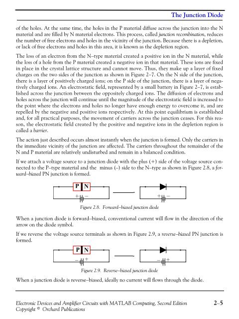
The Junction Diodeof the holes. At the same time, the holes in the P material diffuse across the junction into the Nmaterial and are filled by N material electrons. This process, called junction recombination, reducesthe number of free electrons and holes in the vicinity of the junction. Because there is a depletion,or lack of free electrons and holes in this area, it is known as the depletion region.The loss of an electron from the N−type material created a positive ion in the N material, whilethe loss of a hole from the P material created a negative ion in that material. These ions are fixedin place in the crystal lattice structure and cannot move. Thus, they make up a layer of fixedcharges on the two sides of the junction as shown in Figure 2−7. On the N side of the junction,there is a layer of positively charged ions; on the P side of the junction, there is a layer of negativelycharged ions. An electrostatic field, represented by a small battery in Figure 2−7, is establishedacross the junction between the oppositely charged ions. The diffusion of electrons andholes across the junction will continue until the magnitude of the electrostatic field is increased tothe point where the electrons and holes no longer have enough energy to overcome it, and arerepelled by the negative and positive ions respectively. At this point equilibrium is establishedand, for all practical purposes, the movement of carriers across the junction ceases. For this reason,the electrostatic field created by the positive and negative ions in the depletion region iscalled a barrier.The action just described occurs almost instantly when the junction is formed. Only the carriers inthe immediate vicinity of the junction are affected. The carriers throughout the remainder of theN and P material are relatively undisturbed and remain in a balanced condition.If we attach a voltage source to a junction diode with the plus (+) side of the voltage source connectedto the P−type material and the minus (−) side to the N−type as shown in Figure 2.8, a forward−biasedPN junction is formed.PNFigure 2.8. Forward−biased junction diodeWhen a junction diode is forward−biased, conventional current will flow in the direction of thearrow on the diode symbol.If we reverse the voltage source terminals as shown in Figure 2.9, a reverse−biased PN junction isformed.PNFigure 2.9. Reverse−biased junction diodeWhen a junction diode is reverse−biased, ideally no current will flows through the diode.Electronic Devices and Amplifier Circuits with MATLAB Computing, Second EditionCopyright © Orchard Publications2−5