COMPUTING
Second Edition - Orchard Publications
Second Edition - Orchard Publications
- No tags were found...

Create successful ePaper yourself
Turn your PDF publications into a flip-book with our unique Google optimized e-Paper software.
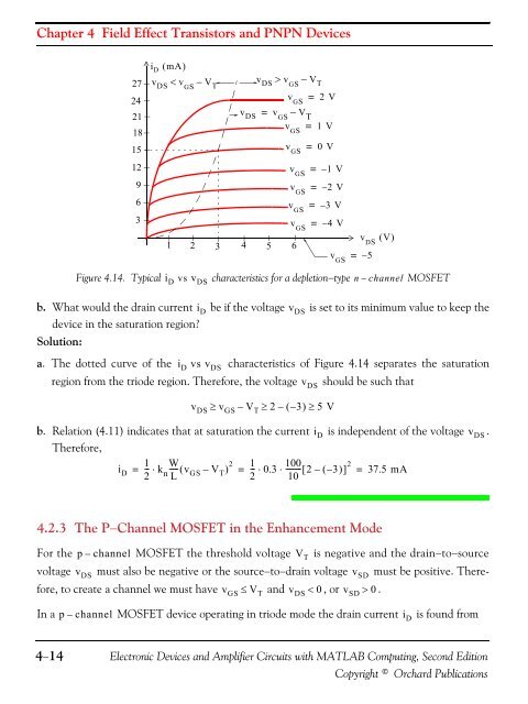
Chapter 4 Field Effect Transistors and PNPN Devices272421181512963i D ( mA)v DS< v GS– V Tv DS> v GS– V Tv GS= 2 Vv DS= v GS– V Tv GS= 1 Vv GSv GSv GSv GSv GS1 2 3 4 5 6=====0 V– 1 V– 2 V– 3 V– 4 Vv DS( V)v GS= – 5Figure 4.14. Typical i D vs v DS characteristics for a depletion−type n – channel MOSFETb. What would the drain current i D be if the voltage v DS is set to its minimum value to keep thedevice in the saturation region?Solution:a. The dotted curve of the i D vs v DS characteristics of Figure 4.14 separates the saturationregion from the triode region. Therefore, the voltage should be such thatv DS ≥ v GS – V T ≥ 2 – (–3)≥ 5 Vb. Relation (4.11) indicates that at saturation the current i D is independent of the voltage v DS .Therefore,1i D--W⋅ k2 n---- ( vL GS – V T ) 2 1 --100= = ⋅0.3 ⋅ -------- [ 2 – (–3)] 2 = 37.5 mA2 10v DS4.2.3 The P−Channel MOSFET in the Enhancement Modev DSFor the p – channel MOSFET the threshold voltage V T is negative and the drain−to−sourcevoltage must also be negative or the source−to−drain voltage must be positive. Therefore,to create a channel we must have ≤ and v DS < 0 , or v SD > 0 .v GSV TIn a p – channel MOSFET device operating in triode mode the drain current i D is found fromv SD4−14Electronic Devices and Amplifier Circuits with MATLAB Computing, Second EditionCopyright © Orchard Publications