

Design Checklist for PowerQUICC II Pro MPC8309 Processor
Design Checklist for PowerQUICC II Pro MPC8309 Processor
Design Checklist for PowerQUICC II Pro MPC8309 Processor

Create successful ePaper yourself
Turn your PDF publications into a flip-book with our unique Google optimized e-Paper software.
JTAG and Debug<br />
5.4 Boot Sequencer<br />
The boot sequencer provides the means to load the hardware reset configuration word and to configure any<br />
memory-mapped register be<strong>for</strong>e the boot-up code runs. Reset configuration loading mode is selected based<br />
on the settings of the CFG_RESET_SOURCE pins during the power-on reset sequence. The I 2 C interface<br />
loads the reset configuration words from an EEPROM at a specific calling address while the rest of the<br />
device is in the reset state. When the reset configuration words are latched inside the device, I 2 C is reset<br />
until HRESET is negated. Then the device is initialized using boot sequencer mode.<br />
Boot sequencer mode is selected at power-on reset by the BOOTSEQ field in the reset configuration word<br />
high register (RCWH). If the boot sequencer mode is selected, the I 2 C module communicates with one or<br />
more EEPROM through the I 2 C interface to initialize one or more configuration register of the <strong>MPC8309</strong>.<br />
For the complete data <strong>for</strong>mat <strong>for</strong> programming the I 2 C EEPROM, refer to <strong>MPC8309</strong> <strong>PowerQUICC</strong> <strong>II</strong> <strong>Pro</strong><br />
Integrated Host <strong>Pro</strong>cessor Reference Manual.<br />
The boot sequencer contains a basic level of error detection. If the I 2 C boot sequencer fails while loading<br />
the reset configuration words are loaded, the RSR[BSF] bit is set. If a preamble or CRC fail is detected in<br />
boot sequencer mode, there is no internal or external indication that the boot sequencer operation failed<br />
Use one of the GPIO pins <strong>for</strong> that purpose.<br />
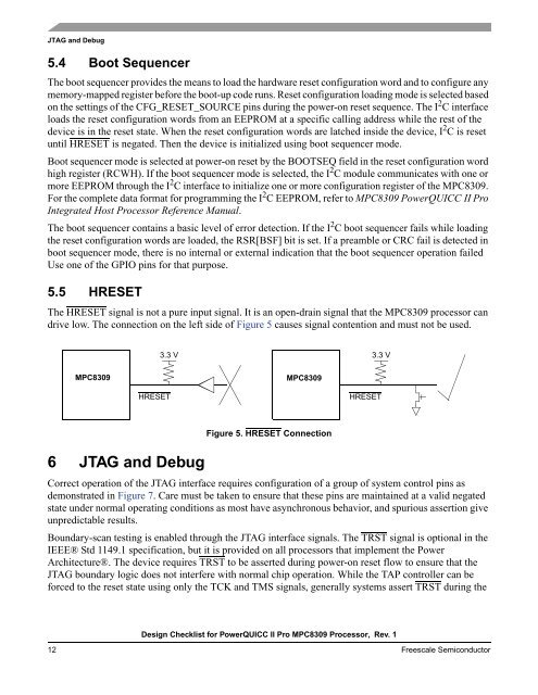
5.5 HRESET<br />
The HRESET signal is not a pure input signal. It is an open-drain signal that the <strong>MPC8309</strong> processor can<br />
drive low. The connection on the left side of Figure 5 causes signal contention and must not be used.<br />
6 JTAG and Debug<br />
3.3 V 3.3 V<br />
<strong>MPC8309</strong> <strong>MPC8309</strong><br />
HRESET HRESET<br />
Figure 5. HRESET Connection<br />
Correct operation of the JTAG interface requires configuration of a group of system control pins as<br />
demonstrated in Figure 7. Care must be taken to ensure that these pins are maintained at a valid negated<br />
state under normal operating conditions as most have asynchronous behavior, and spurious assertion give<br />
unpredictable results.<br />
Boundary-scan testing is enabled through the JTAG interface signals. The TRST signal is optional in the<br />
IEEE® Std 1149.1 specification, but it is provided on all processors that implement the Power<br />
Architecture®. The device requires TRST to be asserted during power-on reset flow to ensure that the<br />
JTAG boundary logic does not interfere with normal chip operation. While the TAP controller can be<br />
<strong>for</strong>ced to the reset state using only the TCK and TMS signals, generally systems assert TRST during the<br />
<strong>Design</strong> <strong>Checklist</strong> <strong>for</strong> <strong>PowerQUICC</strong> <strong>II</strong> <strong>Pro</strong> <strong>MPC8309</strong> <strong>Pro</strong>cessor, Rev. 1<br />
12 Freescale Semiconductor


