

Design Checklist for PowerQUICC II Pro MPC8309 Processor
Design Checklist for PowerQUICC II Pro MPC8309 Processor
Design Checklist for PowerQUICC II Pro MPC8309 Processor

You also want an ePaper? Increase the reach of your titles
YUMPU automatically turns print PDFs into web optimized ePapers that Google loves.
Functional Blocks<br />
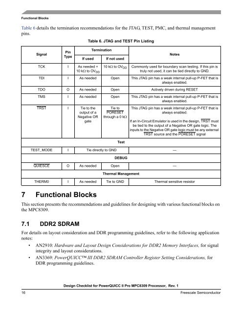
Table 6 details the termination recommendations <strong>for</strong> the JTAG, TEST, PMC, and thermal management<br />
pins.<br />
Signal<br />
Pin<br />
Type<br />
TCK I As needed +<br />
10 k� to OV DD<br />
7 Functional Blocks<br />
This section presents the recommendations and guidelines <strong>for</strong> designing with various functional blocks on<br />
the <strong>MPC8309</strong>.<br />
7.1 DDR2 SDRAM<br />
Table 6. JTAG and TEST Pin Listing<br />
Termination<br />
If used If not used<br />
10 k� to OV DD<br />
For details on layout consideration and DDR programming guidelines, refer to the following application<br />
notes:<br />
• AN2910: Hardware and Layout <strong>Design</strong> Considerations <strong>for</strong> DDR2 Memory Interfaces, <strong>for</strong> signal<br />
integrity and layout considerations.<br />
• AN3369: <strong>PowerQUICC</strong> <strong>II</strong>I DDR2 SDRAM Controller Register Setting Considerations, <strong>for</strong><br />
DDR programming guidelines.<br />
<strong>Design</strong> <strong>Checklist</strong> <strong>for</strong> <strong>PowerQUICC</strong> <strong>II</strong> <strong>Pro</strong> <strong>MPC8309</strong> <strong>Pro</strong>cessor, Rev. 1<br />
16 Freescale Semiconductor<br />
Notes<br />
Commonly used <strong>for</strong> boundary scan testing. If this pin is<br />
truly not used, it can be tied directly to GND.<br />
TDI I As needed Open This JTAG pin has a weak internal pull-up P-FET that is<br />
always enabled.<br />
TDO O As needed Open Actively driven during RESET<br />
TMS I As needed Open This JTAG pin has a weak internal pull-up P-FET that is<br />
always enabled.<br />
TRST I Tie to the<br />
output of a<br />
Negative OR<br />
gate<br />
Tie to<br />
PORESET<br />
through a 0 k�<br />
Test<br />
This JTAG pin has a weak internal pull-up P-FET that is<br />
always enabled.<br />
If an In-Circuit Emulator is used in the design, TRST must<br />
be tied to the output of a Negative OR gate logic. The<br />
inputs to the Negative OR gate logic must be any external<br />
TRST source and the PORESET signal<br />
TEST_MODE I Tie directly to GND —<br />
DEBUG<br />
QUIESCE O As needed Open —<br />
Thermal Management<br />
THERM0 I As needed Tie to GND Thermal sensitive resistor


