Pyxis Layout Suite Datasheet - Mentor Graphics
Pyxis Layout Suite Datasheet - Mentor Graphics
Pyxis Layout Suite Datasheet - Mentor Graphics

Create successful ePaper yourself
Turn your PDF publications into a flip-book with our unique Google optimized e-Paper software.
<strong>Pyxis</strong> <strong>Layout</strong> <strong>Suite</strong><br />
Explore the Possibilities<br />
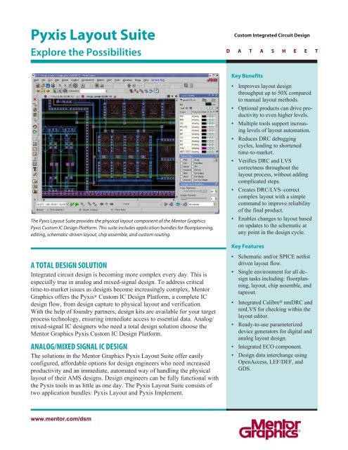
The <strong>Pyxis</strong> <strong>Layout</strong> <strong>Suite</strong> provides the physical layout component of the <strong>Mentor</strong> <strong>Graphics</strong><br />
<strong>Pyxis</strong> Custom IC Design Platform. This suite includes application bundles for floorplanning,<br />
editing, schematic-driven layout, chip assemble, and custom routing.<br />
A TOTAL DESIGN SOLUTION<br />
Integrated circuit design is becoming more complex every day. This is<br />
especially true in analog and mixed-signal design. To address critical<br />
time-to-market issues as designs become increasingly complex, <strong>Mentor</strong><br />
<strong>Graphics</strong> offers the <strong>Pyxis</strong> ® Custom IC Design Platform, a complete IC<br />
design flow, from design capture to physical layout and verification.<br />
With the help of foundry partners, design kits are available for your target<br />
process technology, ensuring immediate access to essential data. Analog/<br />
mixed-signal IC designers who need a total design solution choose the<br />
<strong>Mentor</strong> <strong>Graphics</strong> <strong>Pyxis</strong> Custom IC Design Platform.<br />
ANALOG/MIXED SIGNAL IC DESIGN<br />
The solutions in the <strong>Mentor</strong> <strong>Graphics</strong> <strong>Pyxis</strong> <strong>Layout</strong> <strong>Suite</strong> offer easily<br />
configured, affordable options for design engineers who need increased<br />
productivity and an immediate, automated way of handling the physical<br />
layout of their AMS designs. Design engineers can be fully functional with<br />
the <strong>Pyxis</strong> tools in as little as one day. The <strong>Pyxis</strong> <strong>Layout</strong> <strong>Suite</strong> consists of<br />
two application bundles: <strong>Pyxis</strong> <strong>Layout</strong> and <strong>Pyxis</strong> Implement.<br />
www.mentor.com/dsm<br />
Custom Integrated Circuit Design<br />
D A T A S H E E T<br />
Key Benefits<br />
• Improves layout design<br />
throughput up to 50X compared<br />
to manual layout methods.<br />
• Optional products can drive productivity<br />
to even higher levels.<br />
• Multiple tools support increasing<br />
levels of layout automation.<br />
• Reduces DRC debugging<br />
cycles, leading to shortened<br />
time-to-market.<br />
• Verifies DRC and LVS<br />
correctness throughout the<br />
layout process, without adding<br />
complicated steps.<br />
• Creates DRC/LVS–correct<br />
complex layout with a simple<br />
command to improve reliability<br />
of the final product.<br />
• Enables changes to layout based<br />
on updates to the schematic at<br />
any point in the design cycle.<br />
Key Features<br />
• Schematic and/or SPICE netlist<br />
driven layout flow.<br />
• Single environment for all design<br />
tasks including: floorplanning,<br />
layout, chip assemble, and<br />
tapeout.<br />
• Integrated Calibre ® nmDRC and<br />
nmLVS for checking within the<br />
layout editor.<br />
• Ready-to-use parameterized<br />
device generators for digital and<br />
analog layout design.<br />
• Integrated ECO component.<br />
• Design data interchange using<br />
OpenAccess, LEF/DEF, and<br />
GDS.
These bundles are offered in a standard configuration,<br />
with optional applications that provide increasing levels<br />
of automation and functionality to address the designers<br />
unique requirements. And with <strong>Mentor</strong> <strong>Graphics</strong>,<br />
engineers can be assured they will receive the highest<br />
level of support, training, and technical assistance.<br />
PYXIS LAYOUT<br />
<strong>Pyxis</strong> <strong>Layout</strong> supports an extensive set of editing functions<br />
for efficient, accurate polygon editing. This gives<br />
the engineer full control of circuit density and performance,<br />
while improving productivity by as much as 5X<br />
to help meet time-to-market objectives. Hierarchy and<br />
advanced window management allows multiple views<br />
of the same cell, providing the capability to edit in both<br />
views. And with <strong>Pyxis</strong> <strong>Layout</strong>, engineers can create<br />
matched analog layouts quickly by editing using a halfcell<br />
methodology.<br />
The dynamic alignment and “move as close as possible”<br />
features in <strong>Pyxis</strong> <strong>Layout</strong> enables design engineers<br />
to manipulate layouts from coarse grid resolutions or<br />
large layout views, reducing the number of steps in the<br />
layout process and increasing productivity.<br />
PYXIS IMPLEMENT<br />
Schematic-driven layout (SDL) is a design methodology<br />
that enables design engineers to create “correct<br />
by construction” layouts. These layouts are based on<br />
information from a schematic or a netlist source.<br />
By using the designs connectivity, <strong>Pyxis</strong> Implement<br />
enables the automated creation of layout data, while<br />
maintaining the relationship between layout and schematic,<br />
reducing design cycle time and ensuring layout<br />
is free of LVS violations. Any mix of polygons, device<br />
generators (either custom, built-in or from a foundry<br />
supplied Process Design Kit), and cell data are supported<br />
in the layout environment. <strong>Pyxis</strong> Implement bridges<br />
the gap between schedule and performance goals,<br />
offering productivity increases as much as 50X over<br />
traditional manual layout methods. <strong>Pyxis</strong> Implement<br />
includes all of the functionality of <strong>Pyxis</strong> <strong>Layout</strong>, along<br />
with a hierarchical, SDL environment, enabling design<br />
engineers to quickly create complex designs without<br />
sacrificing layout quality.<br />
www.mentor.com/dsm<br />
Using SDL, design engineers can “pick and place”<br />
devices either automatically or graphically. The dynamic<br />
connectivity display with cross-probing makes<br />
navigation between the layout and schematic fast and<br />
easy. The placed devices can then be quickly connected<br />
using the built in interactive router or the optional<br />
constraint-driven <strong>Pyxis</strong> Customer Router.<br />
The engineering change order (ECO) component of<br />
<strong>Pyxis</strong> Implement quickly modifies the layout to reflect<br />
schematic-driven engineering changes throughout the<br />
design cycle. After comparing the layout with the schematic<br />
source, ECO automatically implements design<br />
changes in the layout and provides an option to correct<br />
the additions, deletions, and property changes, reducing<br />
the time required for layout revisions and keeping<br />
both the schematic and layout design representations<br />
synchronized.<br />
Using the short-checking functionality in <strong>Pyxis</strong> Implement,<br />
design engineers can find potential shorts caused<br />
by overlapping nets before running LVS. Design engineers<br />
can view the shorts in a browsing menu and make<br />
any necessary changes.<br />
Connectivity enables the representation of accurate<br />
layout connections at all times in the design cycle.<br />
Using connectivity throughout the design process<br />
guides designers in creating LVS-correct layout. The<br />
compaction feature in <strong>Pyxis</strong> Implement supports automated<br />
area reduction. Semi- or fully automatic compaction<br />
allows design engineers to increase productivity<br />
without sacrificing layout area. During the design<br />
cycle, connections and placements can be created faster<br />
at loose constraints; then the layout can be post-<br />
processed to achieve tight area constraints.<br />
AUTOMATED DEVICE GENERATION<br />
<strong>Pyxis</strong> Implement supports ready-to-use built-in parameterized<br />
device generators for layout design. Whether<br />
these device generators are provided in a foundry PDK<br />
or created directly by the layout team, they can be<br />
used as is or modified to extend the functionality of<br />
the device. With <strong>Pyxis</strong> Implement, engineers can use<br />
information stored in the schematic source to automatically<br />
create devices that are logically correct and<br />
design-rule–compliant, resulting in a dramatic increase
in productivity over traditional manual method of created<br />
the device from its associated layers.<br />
Devices also can be added and modified manually<br />
through the use of forms and interactive editing commands.<br />
<strong>Pyxis</strong> Implement speeds the creation of designrule–correct<br />
parameterized devices, resulting in designrule–correct<br />
layouts. Custom devices can also be built,<br />
using the base devices as a starting point.<br />
Parameterized layout allows standardization of designs<br />
for multiple engineers and remote sites so that DRC<br />
correct complex layouts can be created with a simple<br />
command, leading to improved productivity.<br />
The transistor device enhances productivity for all<br />
designs, including five, six and “n” pin MOS devices<br />
that support high-voltage devices and complex memory<br />
designs using bent gates. Transistor editing commands<br />
offer enhanced flexibility for intricate designs without<br />
destroying the device, improving productivity and reliability.<br />
The capacitor device creates complex capacitors<br />
used in switch capacitors, with a single command,<br />
for increased productivity.<br />
The shape-based capacitor device allows design engineers<br />
to “fill” areas with capacitors for area savings,<br />
and increase flexibility for future design changes. The<br />
via device, with mltiple subtypes, supports DFM rules<br />
as well as “inline” or “turn” routing level transitions<br />
in advanced geometry technologies with automatic via<br />
selection and rotation. The resistor device supports<br />
multiple processes, as well as series and parallel structures.<br />
Matched resistors are created with a single command.<br />
The guardband device enables design engineers<br />
to quickly shield sensitive analog layouts. Guardband<br />
editing commands include a cutting ability to complete<br />
routing through the guardband to sensitive analog layouts,<br />
increasing productivity.<br />
FLOORPLANNING<br />
As the complexity of today’s mixed-signal SOC designs<br />
continue to grow, planning before layout plays an<br />
ever important role. This floorplanning step is supported<br />
by <strong>Pyxis</strong> Assemble, which is completely integrated<br />
within the layout environment. Advanced floor planning<br />
features include:<br />
www.mentor.com/dsm<br />
• Multiple area estimation modes.<br />
• <strong>Layout</strong> wire propagation (push/pull through hierarchy<br />
with connectivity).<br />
• Hierarchy management.<br />
• ECO flow integration.<br />
• Top-down block boundary editing ability.<br />
• Input from <strong>Pyxis</strong> Schematic, SPICE netlist, Verilog<br />
netlist.<br />
• Read/write LEF/DEF blocks.<br />
MULTIPLE DESIGNER LAYOUT<br />
<strong>Mentor</strong> <strong>Graphics</strong> developed the optional <strong>Pyxis</strong><br />
Concurrent environment that enables multiple designer<br />
to simultaneously edit the same cell. This is targeted<br />
for the final stages of the project, where assemble and<br />
DRC/LVS clean-up are being finalized just before tapeout.<br />
For more information on this solution, please refer<br />
to the <strong>Pyxis</strong> Concurrent datasheet.<br />
LAYOUT AUTOMATION<br />
The interactive routing capabilities of <strong>Pyxis</strong> <strong>Layout</strong><br />
<strong>Suite</strong> include:<br />
• Truly integrated routing technology with pushing<br />
for “routing in place.”<br />
• Flexible blockage control.<br />
• On-the-fly visual feedback of length, resistance,<br />
capacitance, or costing.<br />
• Intelligent minimization of nets being pushed.<br />
• Multiple bus routing modes.<br />
• Control wire handling for critical nets.<br />
Supported post-routing based DFM improvements in<br />
<strong>Pyxis</strong> <strong>Layout</strong> <strong>Suite</strong> include:<br />
• Via minimization.<br />
• Layer swapping.<br />
• Wire bend reduction.<br />
The optional <strong>Pyxis</strong> Custom Router was developed to<br />
meet the routing needs for today’s analog designs. It’s<br />
a constraint-driven router that has been qualified at<br />
28 nm. For more information, see the <strong>Pyxis</strong> Custom<br />
Router datasheet.<br />
As the digital content in today’s mixed-signal SOC<br />
designs continues to grow, top-level floorplanning and<br />
routing becomes an important component in the design
flow. <strong>Mentor</strong> <strong>Graphics</strong> developed <strong>Pyxis</strong> Assemble,<br />
which provides a robust set of features for floorplanning,<br />
top-level assembly, and interactive routing.<br />
OTHER CUSTOM METHODOLOGIES<br />
The <strong>Pyxis</strong> <strong>Layout</strong> <strong>Suite</strong> can be customized to support<br />
complex design methodologies. The first of these<br />
customizations is for MeMs. One of the unique capabilities<br />
included in the <strong>Pyxis</strong> <strong>Layout</strong> <strong>Suite</strong> is the ability<br />
for any angle rotation, which is a common operation<br />
with MeMs design. The second customization is for the<br />
layout of flat panels. An optional product in the <strong>Pyxis</strong><br />
<strong>Layout</strong> <strong>Suite</strong>, <strong>Pyxis</strong> TFT-LCD, supports same-length<br />
and same-layer routing as well as other panel specific<br />
design features.<br />
Visit our website at www.mentor.com/dsm<br />
Copyright © 2011 <strong>Mentor</strong> <strong>Graphics</strong> Corporation. <strong>Mentor</strong> products and processes are registered trademarks of <strong>Mentor</strong> <strong>Graphics</strong> Corporation.<br />
All other trademarks mentioned in this document are trademarks of their respective owners.<br />
Corporate Headquarters<br />
<strong>Mentor</strong> <strong>Graphics</strong><br />
Corporation<br />
8005 S.W. Boeckman Road<br />
Wilsonville, Oregon<br />
97070-7777<br />
Phone: 503-685-7000<br />
Fax: 503-685-1204<br />
Sales and Product<br />
Information<br />
Phone: 800-547-3000<br />
Silicon Valley<br />
<strong>Mentor</strong> <strong>Graphics</strong><br />
Corporation<br />
46871 Bayside Parkway<br />
Fremont California 94538 USA<br />
Phone: 510-354-7400<br />
Fax: 510-354-7467<br />
North American<br />
Support Center<br />
Phone: 800-547-4303<br />
Europe<br />
<strong>Mentor</strong> <strong>Graphics</strong><br />
Deutschland GmbH<br />
Arnulfstrasse 201<br />
80634 Munich<br />
Germany<br />
Phone: +49.89.57096.0<br />
Fax: +49.89.57096.400<br />
DESIGN DATA INTERCHANGE<br />
<strong>Pyxis</strong> <strong>Layout</strong> suite supports the interchange of design<br />
data through industry standard formats. The supported<br />
formats are OpenAccess, LEF/DEF, and GDS.<br />
LAYOUT VERIFICATION<br />
Integration with Calibre RealTime provides<br />
Calibre signoff-quality physical verification, ondemand,<br />
within the <strong>Mentor</strong> <strong>Graphics</strong> <strong>Pyxis</strong> Custom<br />
IC Design Platform. Using the same Calibre decks as<br />
the signoff flow, design engineers can now verify and<br />
optimize their designs while they edit their layouts.<br />
With Calibre RealTime, designers can optimize their<br />
layouts for performance without sacrificing manufacturing<br />
yield.<br />
The <strong>Mentor</strong> <strong>Graphics</strong> Custom IC flow and its integrated schematic, extraction, and<br />
simulation tools allow you to take a design from system specifications to post-layout<br />
verification with a virtually seamless approach.<br />
Pacific Rim<br />
<strong>Mentor</strong> <strong>Graphics</strong> Taiwan<br />
Room 1001, 10F,<br />
International Trade Building<br />
No. 333, Section 1, Keelung Road<br />
Taipei, Taiwan, ROC<br />
Phone: 886-2-87252000<br />
Fax: 886-2-27576027<br />
Japan<br />
<strong>Mentor</strong> <strong>Graphics</strong> Japan<br />
Co., Ltd.<br />
Gotenyama Garden<br />
7-35, Kita-Shinagawa 4-chome<br />
Shinagawa-Ku, Tokyo 140 -0001<br />
Japan<br />
Phone: 81-3-5488-3033<br />
Fax: 81-3-5488-3004<br />
7-11-MGC 1029590