

Infineon SAB 80C517A, SAB 83C517A-5 User's Manual ... - Keil
Infineon SAB 80C517A, SAB 83C517A-5 User's Manual ... - Keil
Infineon SAB 80C517A, SAB 83C517A-5 User's Manual ... - Keil

You also want an ePaper? Increase the reach of your titles
YUMPU automatically turns print PDFs into web optimized ePapers that Google loves.
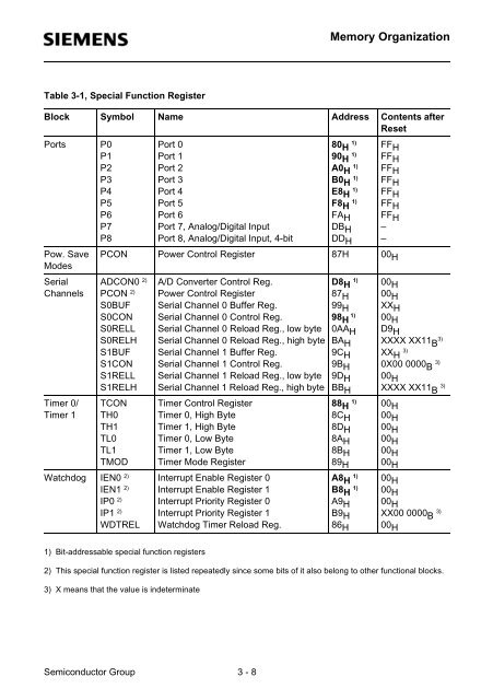
Table 3-1, Special Function Register<br />
1) Bit-addressable special function registers<br />
Semiconductor Group 3 - 8<br />
Memory Organization<br />
Block Symbol Name Address Contents after<br />
Reset<br />
Ports P0<br />
P1<br />
P2<br />
P3<br />
P4<br />
P5<br />
P6<br />
P7<br />
P8<br />
Pow. Save<br />
Modes<br />
Serial<br />
Channels<br />
Timer 0/<br />
Timer 1<br />
2) This special function register is listed repeatedly since some bits of it also belong to other functional blocks.<br />
3) X means that the value is indeterminate<br />
Port 0<br />
Port 1<br />
Port 2<br />
Port 3<br />
Port 4<br />
Port 5<br />
Port 6<br />
Port 7, Analog/Digital Input<br />
Port 8, Analog/Digital Input, 4-bit<br />
80 H 1)<br />
90 H 1)<br />
A0 H 1)<br />
B0 H 1)<br />
E8 H 1)<br />
F8 H 1)<br />
FA H<br />
DB H<br />
DD H<br />
FF H<br />
FF H<br />
FF H<br />
FF H<br />
FF H<br />
FF H<br />
FF H<br />
–<br />
–<br />
PCON Power Control Register 87H 00 H<br />
ADCON0 2)<br />
PCON 2)<br />
S0BUF<br />
S0CON<br />
S0RELL<br />
S0RELH<br />
S1BUF<br />
S1CON<br />
S1RELL<br />
S1RELH<br />
TCON<br />
TH0<br />
TH1<br />
TL0<br />
TL1<br />
TMOD<br />
Watchdog IEN0 2)<br />
IEN1 2)<br />
IP0 2)<br />
IP1 2)<br />
WDTREL<br />
A/D Converter Control Reg.<br />
Power Control Register<br />
Serial Channel 0 Buffer Reg.<br />
Serial Channel 0 Control Reg.<br />
Serial Channel 0 Reload Reg., low byte<br />
Serial Channel 0 Reload Reg., high byte<br />
Serial Channel 1 Buffer Reg.<br />
Serial Channel 1 Control Reg.<br />
Serial Channel 1 Reload Reg., low byte<br />
Serial Channel 1 Reload Reg., high byte<br />
Timer Control Register<br />
Timer 0, High Byte<br />
Timer 1, High Byte<br />
Timer 0, Low Byte<br />
Timer 1, Low Byte<br />
Timer Mode Register<br />
Interrupt Enable Register 0<br />
Interrupt Enable Register 1<br />
Interrupt Priority Register 0<br />
Interrupt Priority Register 1<br />
Watchdog Timer Reload Reg.<br />
D8 H 1)<br />
87 H<br />
99 H<br />
98 H 1)<br />
0AA H<br />
BA H<br />
9C H<br />
9B H<br />
9D H<br />
BB H<br />
88 H 1)<br />
8C H<br />
8D H<br />
8A H<br />
8B H<br />
89 H<br />
A8 H 1)<br />
B8 H 1)<br />
A9 H<br />
B9 H<br />
86 H<br />
00 H<br />
00 H<br />
XX H<br />
00 H<br />
D9 H<br />
XXXX XX11 B 3)<br />
XX H 3)<br />
0X00 0000 B 3)<br />
00 H<br />
XXXX XX11 B 3)<br />
00 H<br />
00 H<br />
00 H<br />
00 H<br />
00 H<br />
00 H<br />
00 H<br />
00 H<br />
00 H<br />
XX00 0000 B 3)<br />
00 H


