- Page 1 and 2: Microcomputer Components SAB 80C517
- Page 3 and 4: SAB 80C517A/83C517A-5 Revision Hist
- Page 5 and 6: 1 Introduction The SAB 80C517A is a
- Page 7 and 8: 2 Fundamental Structure The SAB 80C
- Page 9 and 10: 3 Memory Organization Semiconductor
- Page 11 and 12: 3.2 Data Memory Semiconductor Group
- Page 13 and 14: Table 3-1, Special Function Registe
- Page 15 and 16: Table 3-1, Special Function Registe
- Page 17 and 18: 3.4 Architecture for the XRAM Semic
- Page 19 and 20: Figure 3-2 Write Page Address to Po
- Page 21 and 22: Figure 3-4 Use of Port 2 as I/O-Por
- Page 23 and 24: 3.4.2 Control of XRAM in the SAB 80
- Page 25 and 26: EA = 0 EA = 1 XMAP1, XMAP0 XMAP1, X
- Page 27 and 28: Table 4-1, Status of all Pins Durin
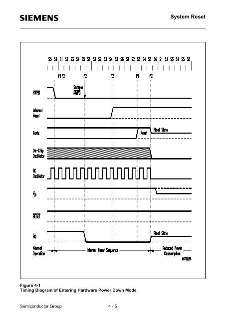
- Page 29: 4.2 Hardware Power Down Reset Timin
- Page 33 and 34: 4.3 Fast internal Reset after Power
- Page 35 and 36: Figure 4-4 Power-On of the SAB 80C5
- Page 37 and 38: Semiconductor Group 5 - 2 On-Chip P
- Page 39 and 40: Figure 5-1 10-Bit A/D-Converter Sem
- Page 41 and 42: Special Function Register ADDATH, A
- Page 43 and 44: 5.3 Additional Compare Mode for the
- Page 45 and 46: Special Function Register CC4EN Bit
- Page 47 and 48: Semiconductor Group 5 - 12 On-Chip
- Page 49 and 50: Semiconductor Group 5 - 14 On-Chip
- Page 51 and 52: Semiconductor Group 5 - 16 On-Chip
- Page 53 and 54: Special Function Register SRELH, SR
- Page 55 and 56: Detailled Description of the Oscill
- Page 57 and 58: 6 Interrupt System 6.1 Additional I
- Page 59 and 60: Special Function Register IRCON1 Bi
- Page 61 and 62: 3.1 Priority Level Structure The fo
- Page 63 and 64: 4 Device Specification Device Speci
- Page 65 and 66: Logic Symbol Semiconductor Group 7-
- Page 67 and 68: Pin Configuration (P-MQFP-100-2) Se
- Page 69 and 70: Pin Definitions and Functions (cont
- Page 71 and 72: Pin Definitions and Functions (cont
- Page 73 and 74: Pin Definitions and Functions (cont
- Page 75 and 76: Pin Definitions and Functions (cont
- Page 77 and 78: Figure 1 Block Diagram Semiconducto
- Page 79 and 80: Semiconductor Group 7-17 Device Spe
- Page 81 and 82:
Semiconductor Group 7-19 Device Spe
- Page 83 and 84:
Semiconductor Group 7-21 Device Spe
- Page 85 and 86:
s Table 1: Behaviour of P0/P2 and R
- Page 87 and 88:
Semiconductor Group 7-25 Device Spe
- Page 89 and 90:
Table 2 Special Function Register (
- Page 91 and 92:
Table 3 Special Function Registers
- Page 93 and 94:
Table 3 Special Function Registers
- Page 95 and 96:
Figure 4 Block Diagram A/D Converte
- Page 97 and 98:
Table 4 CCU Compare Configuration S
- Page 99 and 100:
Semiconductor Group 7-37 Device Spe
- Page 101 and 102:
Figure 6 Block Diagram of Timer 2 S
- Page 103 and 104:
Figure 9 Compare-Mode 2 (Port 5 onl
- Page 105 and 106:
Figure 10 Interrupt Structure of th
- Page 107 and 108:
Figure 10 Interrupt Structure of th
- Page 109 and 110:
Table 6 Performing a MDU-Calculatio
- Page 111 and 112:
Semiconductor Group 7-49 Device Spe
- Page 113 and 114:
Semiconductor Group 7-51 Device Spe
- Page 115 and 116:
Semiconductor Group 7-53 Device Spe
- Page 117 and 118:
Serial Interface 0 Serial Interface
- Page 119 and 120:
Semiconductor Group 7-57 Device Spe
- Page 121 and 122:
Figure 12 Functional Block Diagram
- Page 123 and 124:
Semiconductor Group 7-61 Device Spe
- Page 125 and 126:
Semiconductor Group 7-63 Device Spe
- Page 127 and 128:
Semiconductor Group 7-65 Device Spe
- Page 129 and 130:
ALE PSEN Port 0 Port 2 Program Memo
- Page 131 and 132:
AC Characteristics (cont’d) Exter
- Page 133 and 134:
ROM Verification Characteristics TA
- Page 135 and 136:
Application Circuitry for Verifying
- Page 137:
Package Outlines Plastic Package, P