

Infineon SAB 80C517A, SAB 83C517A-5 User's Manual ... - Keil
Infineon SAB 80C517A, SAB 83C517A-5 User's Manual ... - Keil
Infineon SAB 80C517A, SAB 83C517A-5 User's Manual ... - Keil

You also want an ePaper? Increase the reach of your titles
YUMPU automatically turns print PDFs into web optimized ePapers that Google loves.
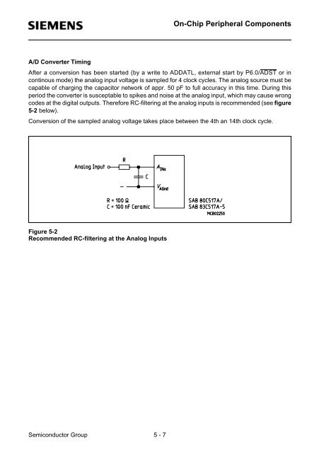
A/D Converter Timing<br />
Semiconductor Group 5 - 7<br />
On-Chip Peripheral Components<br />
After a conversion has been started (by a write to ADDATL, external start by P6.0/ADST or in<br />
continous mode) the analog input voltage is sampled for 4 clock cycles. The analog source must be<br />
capable of charging the capacitor network of appr. 50 pF to full accuracy in this time. During this<br />
period the converter is susceptable to spikes and noise at the analog input, which may cause wrong<br />
codes at the digital outputs. Therefore RC-filtering at the analog inputs is recommended (see figure<br />
5-2 below).<br />
Conversion of the sampled analog voltage takes place between the 4th an 14th clock cycle.<br />
Figure 5-2<br />
Recommended RC-filtering at the Analog Inputs


