

Infineon SAB 80C517A, SAB 83C517A-5 User's Manual ... - Keil
Infineon SAB 80C517A, SAB 83C517A-5 User's Manual ... - Keil
Infineon SAB 80C517A, SAB 83C517A-5 User's Manual ... - Keil

Create successful ePaper yourself
Turn your PDF publications into a flip-book with our unique Google optimized e-Paper software.
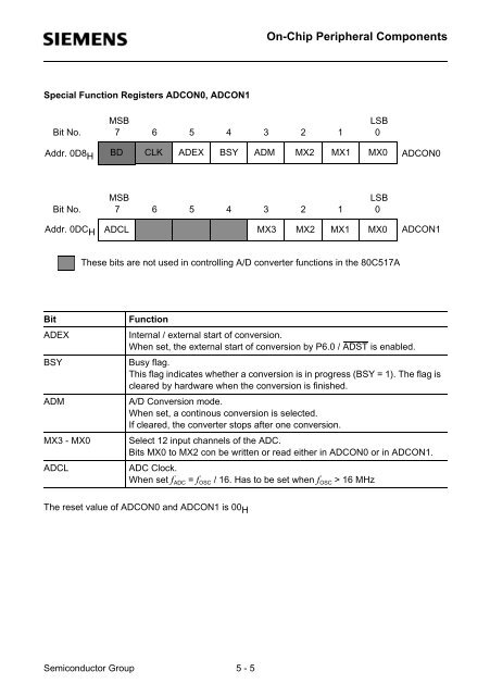
Special Function Registers ADCON0, ADCON1<br />
Bit No.<br />
Addr. 0D8 H<br />
Bit No.<br />
Addr. 0DC H<br />
The reset value of ADCON0 and ADCON1 is 00 H<br />
Semiconductor Group 5 - 5<br />
On-Chip Peripheral Components<br />
MSB LSB<br />
7 6 5 4 3 2 1 0<br />
BD CLK ADEX BSY ADM MX2 MX1 MX0<br />
MSB LSB<br />
7 6 5 4 3 2 1 0<br />
ADCL MX3<br />
MX2 MX1 MX0<br />
These bits are not used in controlling A/D converter functions in the <strong>80C517A</strong><br />
ADCON0<br />
ADCON1<br />
Bit Function<br />
ADEX Internal / external start of conversion.<br />
When set, the external start of conversion by P6.0 / ADST is enabled.<br />
BSY Busy flag.<br />
This flag indicates whether a conversion is in progress (BSY = 1). The flag is<br />
cleared by hardware when the conversion is finished.<br />
ADM A/D Conversion mode.<br />
When set, a continous conversion is selected.<br />
If cleared, the converter stops after one conversion.<br />
MX3 - MX0 Select 12 input channels of the ADC.<br />
Bits MX0 to MX2 con be written or read either in ADCON0 or in ADCON1.<br />
ADCL ADC Clock.<br />
When set fADC = fOSC / 16. Has to be set when fOSC > 16 MHz


