Infineon SAB 80C517A, SAB 83C517A-5 User's Manual ... - Keil
Infineon SAB 80C517A, SAB 83C517A-5 User's Manual ... - Keil
Infineon SAB 80C517A, SAB 83C517A-5 User's Manual ... - Keil
You also want an ePaper? Increase the reach of your titles
YUMPU automatically turns print PDFs into web optimized ePapers that Google loves.
Semiconductor Group 3 - 14<br />
Memory Organization<br />
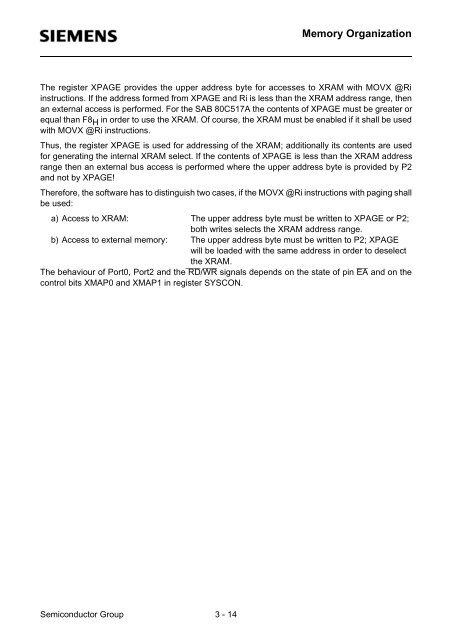
The register XPAGE provides the upper address byte for accesses to XRAM with MOVX @Ri<br />
instructions. If the address formed from XPAGE and Ri is less than the XRAM address range, then<br />
an external access is performed. For the <strong>SAB</strong> <strong>80C517A</strong> the contents of XPAGE must be greater or<br />
equal than F8H in order to use the XRAM. Of course, the XRAM must be enabled if it shall be used<br />
with MOVX @Ri instructions.<br />
Thus, the register XPAGE is used for addressing of the XRAM; additionally its contents are used<br />
for generating the internal XRAM select. If the contents of XPAGE is less than the XRAM address<br />
range then an external bus access is performed where the upper address byte is provided by P2<br />
and not by XPAGE!<br />
Therefore, the software has to distinguish two cases, if the MOVX @Ri instructions with paging shall<br />
be used:<br />
a) Access to XRAM: The upper address byte must be written to XPAGE or P2;<br />
both writes selects the XRAM address range.<br />
b) Access to external memory: The upper address byte must be written to P2; XPAGE<br />
will be loaded with the same address in order to deselect<br />
the XRAM.<br />
The behaviour of Port0, Port2 and the RD/WR signals depends on the state of pin EA and on the<br />
control bits XMAP0 and XMAP1 in register SYSCON.


