Infineon SAB 80C517A, SAB 83C517A-5 User's Manual ... - Keil
Infineon SAB 80C517A, SAB 83C517A-5 User's Manual ... - Keil
Infineon SAB 80C517A, SAB 83C517A-5 User's Manual ... - Keil
Create successful ePaper yourself
Turn your PDF publications into a flip-book with our unique Google optimized e-Paper software.
Semiconductor Group 3 - 16<br />
Memory Organization<br />
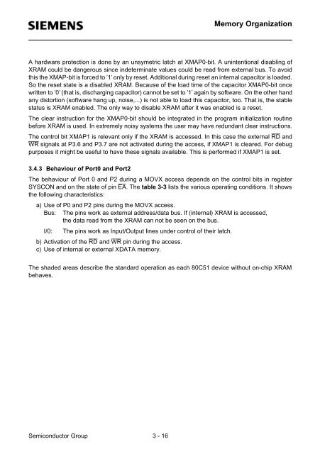
A hardware protection is done by an unsymetric latch at XMAP0-bit. A unintentional disabling of<br />
XRAM could be dangerous since indeterminate values could be read from external bus. To avoid<br />
this the XMAP-bit is forced to ’1’ only by reset. Additional during reset an internal capacitor is loaded.<br />
So the reset state is a disabled XRAM. Because of the load time of the capacitor XMAP0-bit once<br />
written to ’0’ (that is, discharging capacitor) cannot be set to ’1’ again by software. On the other hand<br />
any distortion (software hang up, noise,...) is not able to load this capacitor, too. That is, the stable<br />
status is XRAM enabled. The only way to disable XRAM after it was enabled is a reset.<br />
The clear instruction for the XMAP0-bit should be integrated in the program initialization routine<br />
before XRAM is used. In extremely noisy systems the user may have redundant clear instructions.<br />
The control bit XMAP1 is relevant only if the XRAM is accessed. In this case the external RD and<br />
WR signals at P3.6 and P3.7 are not activated during the access, if XMAP1 is cleared. For debug<br />
purposes it might be useful to have these signals available. This is performed if XMAP1 is set.<br />
3.4.3 Behaviour of Port0 and Port2<br />
The behaviour of Port 0 and P2 during a MOVX access depends on the control bits in register<br />
SYSCON and on the state of pin EA. The table 3-3 lists the various operating conditions. It shows<br />
the following characteristics:<br />
a) Use of P0 and P2 pins during the MOVX access.<br />
Bus: The pins work as external address/data bus. If (internal) XRAM is accessed,<br />
the data read from the XRAM can not be seen on the bus.<br />
I/0: The pins work as Input/Output lines under control of their latch.<br />
b) Activation of the RD and WR pin during the access.<br />
c) Use of internal or external XDATA memory.<br />
The shaded areas describe the standard operation as each 80C51 device without on-chip XRAM<br />
behaves.


