4-2017
Fachzeitschrift für Hochfrequenz- und Mikrowellentechnik
Fachzeitschrift für Hochfrequenz- und Mikrowellentechnik

Sie wollen auch ein ePaper? Erhöhen Sie die Reichweite Ihrer Titel.
YUMPU macht aus Druck-PDFs automatisch weboptimierte ePaper, die Google liebt.
Rubriken<br />
Test & Measurement<br />
Immunity and Emissions Scanning for EMC<br />
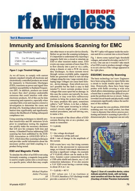
Figure 1: Logic Threshold Voltages<br />
As we all know, to comply with current<br />
industry standard virtually all electronic and<br />
electronically controlled products are tested<br />
for immunity to Electrostatic Discharges<br />
(ESD), transients on power and signal lines<br />
and their susceptibility to Radiated Frequencies<br />
(RF). In addition, products are tested<br />
in insure they don’t produce undesirable<br />
emissions that could interfere with other<br />
electronic products. All of this can be time<br />
consuming and expensive, especially when<br />
a product fails a test and requires extensive<br />
investigation to determine the cause and<br />
develop a fix. Scanning reduces test and evaluation<br />
time significantly and significantly<br />
reduces the likelihood of failing subsequent<br />
compliance test.<br />
Using scanning techniques to identify product<br />
sensitivities and RF emissions levels<br />
prior to compliance testing the engineer<br />
can quickly make the necessary decisions<br />
that will save his company both time and<br />
money. A Standard Practice addressing ESD<br />
scanning has been published by the EOS/<br />
ESD Association as ANSI/ESD SP14.5-<br />
2015, which describes scanning techniques<br />
and provides useful information about the<br />
necessary probes and field coupling to a<br />
product being tested.<br />
ESD and Magnetic Fields<br />
To simulate the effect of an ESD event using<br />
Immunity scanning, a magnetic loop probe<br />
is used to couple a pulse onto a circuit trace<br />
at a specific point, which then may couple<br />
Michael Hopkins<br />
Amber Precision<br />
AR<br />
www.arworld.us<br />
into other traces or an active device directly.<br />
Before we get into the scanning techniques,<br />
it’s important to understand why injecting a<br />
magnetic field into a circuit to simulate an<br />
ESD or other transient makes sense. ESD<br />
events can cause currents of more than 50 A<br />
to flow directly into a port or via a cable,<br />
along a chassis or onto a PCB via secondary<br />
discharges. As these currents travel<br />
through various available paths, magnetic<br />
fields are generated which in turn develop<br />
voltages along the way. Large currents developing<br />
large voltages can cause hard failures<br />
– device damage - from which recovery<br />
isn’t possible but the fault is easy to find<br />
(smoke?!); lower currents produce lower<br />
voltages that cause upset but no damage. In<br />
this case the system can typically be reset,<br />
rebooted, or may even have selfrecovery<br />
routines to bring the system back on-line.<br />
For many products this upset, sometimes<br />
called a “soft” failure, is in fact, a failure.<br />
Think of what upset occurring in critical<br />
control circuits might cause – avionics,<br />
medical procedures, and self-driving cars,<br />
to name a few.<br />
As an example of the direct effect of ESD<br />
currents flowing into or on a product, one<br />
needs to remember:<br />
V= L(di/dt)<br />
Where<br />
V = the voltage developed<br />
L = Inductance of the path and<br />
di/dt = rate of change in the amplitude of<br />
the current.<br />
ESD events have very fast rising currents<br />
that are in the picosecond to nanosecond<br />
range, so it doesn’t take much inductance to<br />
develop a significant voltage. An example<br />
of V=L(di/dt) effects can be made as follows:<br />
Assume a poor connection between<br />
a USB cable shield and chassis, say a 2 nH<br />
connection inductance. If we also assume<br />
a 5 kV ESD event having a current rising<br />
to about 20 A in 1 ns:<br />
V = L(di/dt) = 40 V!<br />
( IEC values are: 1.2 ns risetimes at<br />
3.75 A/kV; therefore a 5 kV discharge would<br />
provide a current of 18.75 A.)<br />
The 40 V spike will appear inside the enclosure<br />
and drive a current into a circuit board.<br />
Fig. 1 shows some typical logic threshold<br />
voltages, and actual levels today can be 0.3 V<br />
or less. One can see it wouldn’t take much<br />
of an ESD event to produce enough voltage<br />
to re-set a device if the voltage appeared in<br />
the right place.<br />
ESD/EMC Immunity Scanning<br />
The basic technology isn’t new: Engineers<br />
have been using probes to inject fields into<br />
a circuit to locate trouble spots for some<br />
time. Historically, these have been large<br />
probes with fields covering a wide area<br />
which allows determining a general area of<br />
a board that is sensitive but difficult to pinpoint<br />
the problem device or circuit. Todays<br />
crowded circuit boards and physically small<br />
components significantly reduce the usefulness<br />
of this method.<br />
To get around the size problem, ESD/EMI<br />
scanning uses very small probes, less than<br />
1 mm in diameter that allows precise positioning<br />
and iterative scanning to provide a 3<br />
dimensional plot. An engineer can not only<br />
Figure 2: Scan of a sensitive device, colors<br />
indicate sensitivity levels, with red being<br />
most sensitive and blue the least sensitive<br />
(Courtesy of Amber Precision Instruments)<br />
hf-praxis 4/<strong>2017</strong> 79